
Aerosol Jet Printing of 3D Pillar Arrays from Photopolymer Ink

 , , , and
Abstract
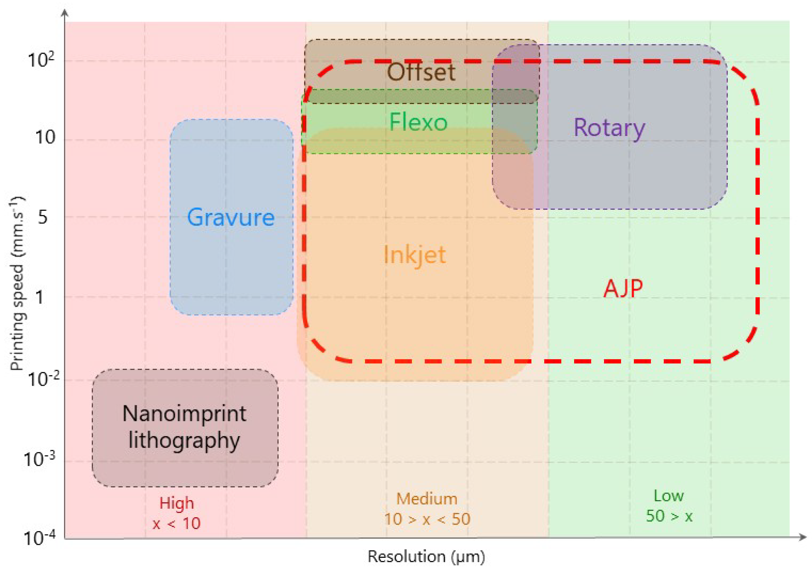
:1. Introduction
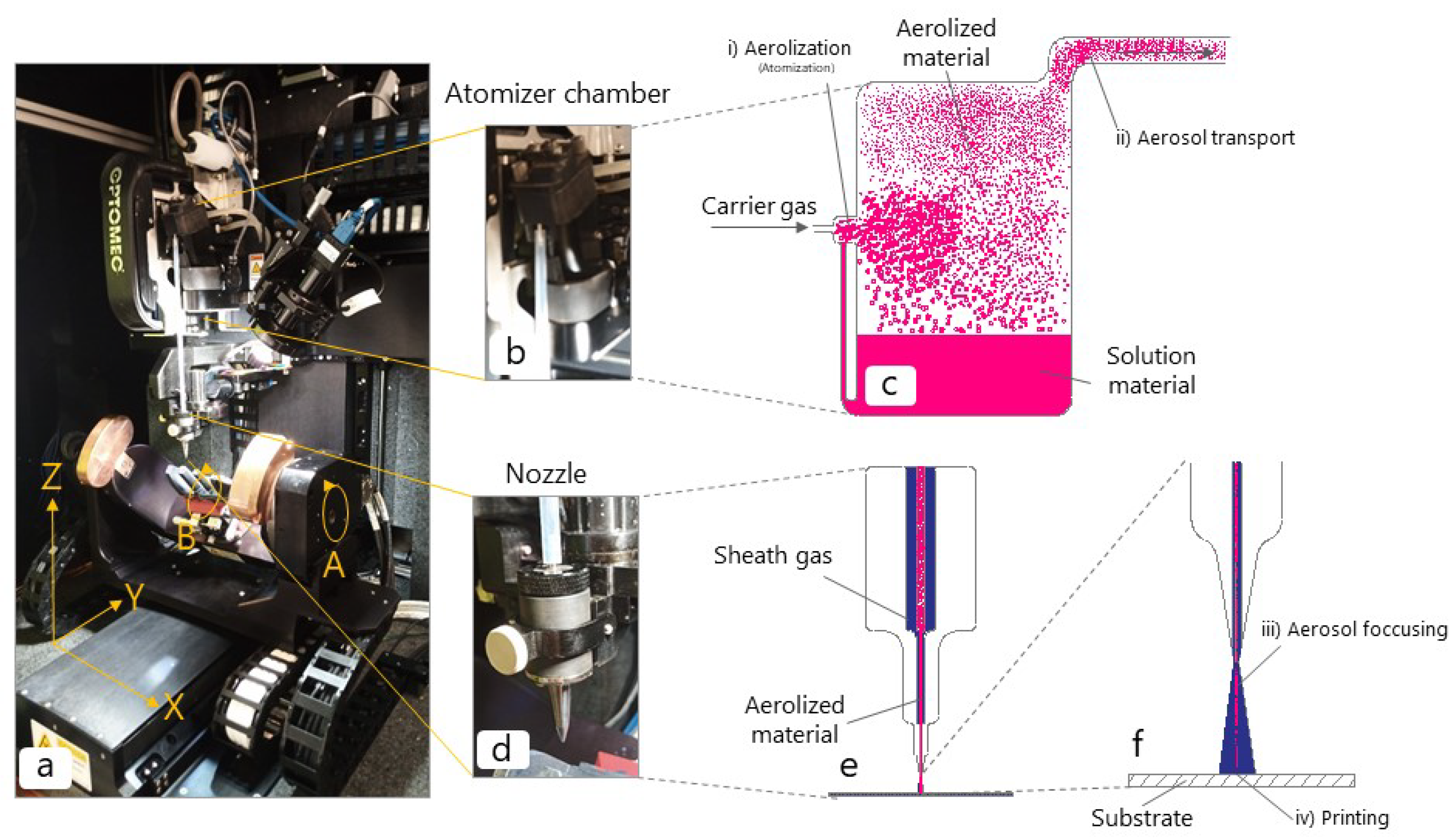
Aerosol Jet Printing—AJP
- (i)
- Ink aerosolization;
- (ii)
- Aerosol transport by a carrier gas;
- (iii)
- Aerosol focusing;
- (iv)
- Material transfer to the substrate.

2. Materials and Methods
2.1. Materials
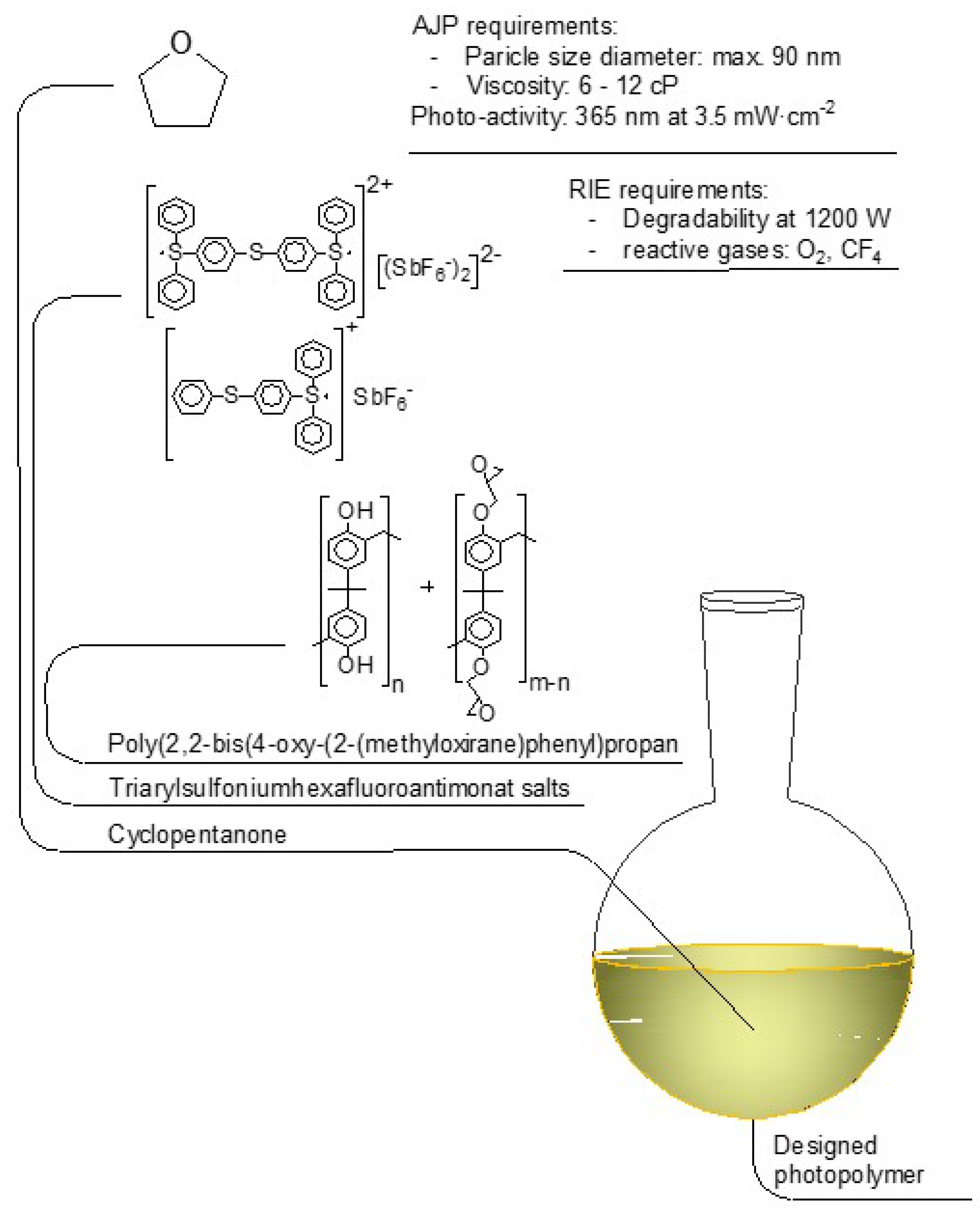
2.2. Photopolymer Formulation
2.3. Aerosol Jet Printing
2.4. Reactive Ion Etching (RIE)
2.5. Scanning Electron Microscopy
3. Results and Discussion
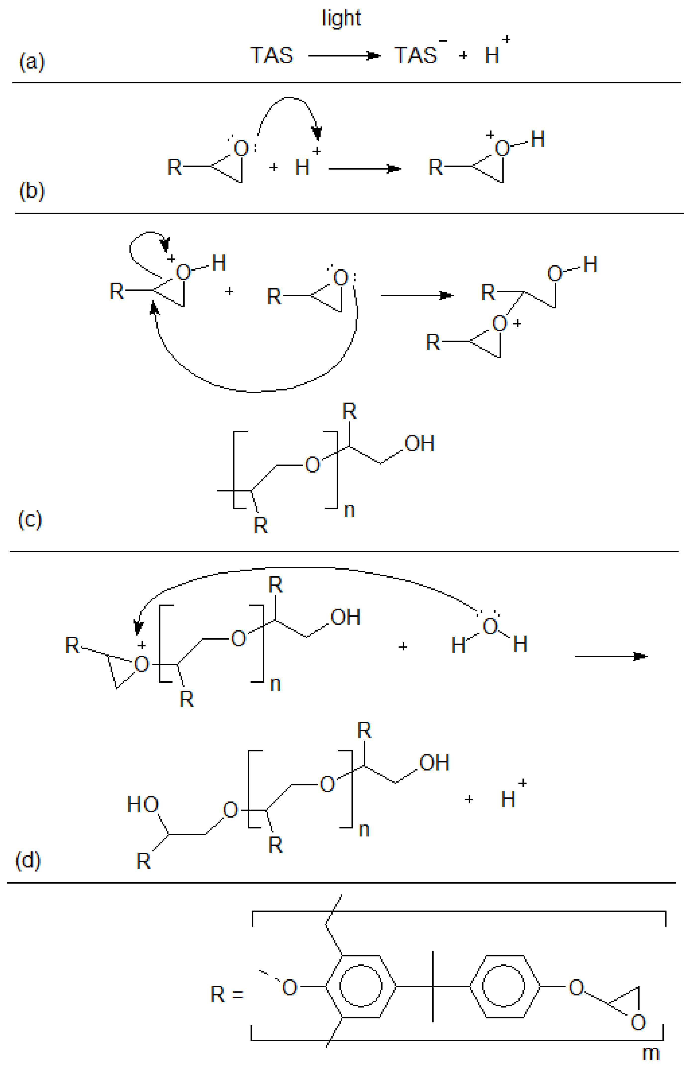
3.1. Photopolymer Design
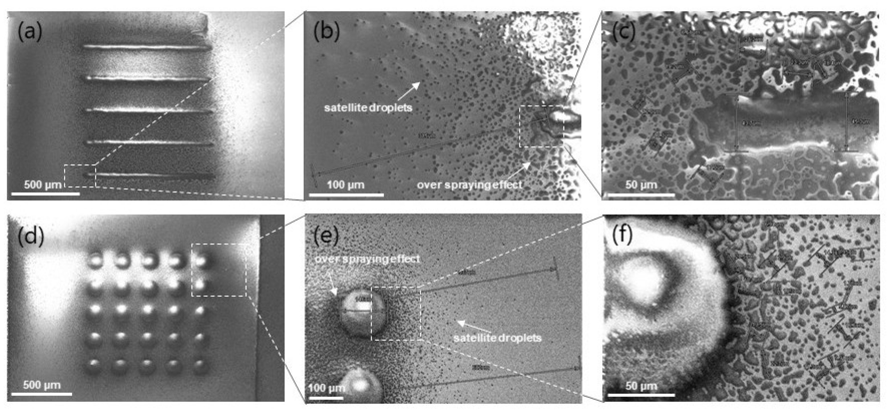
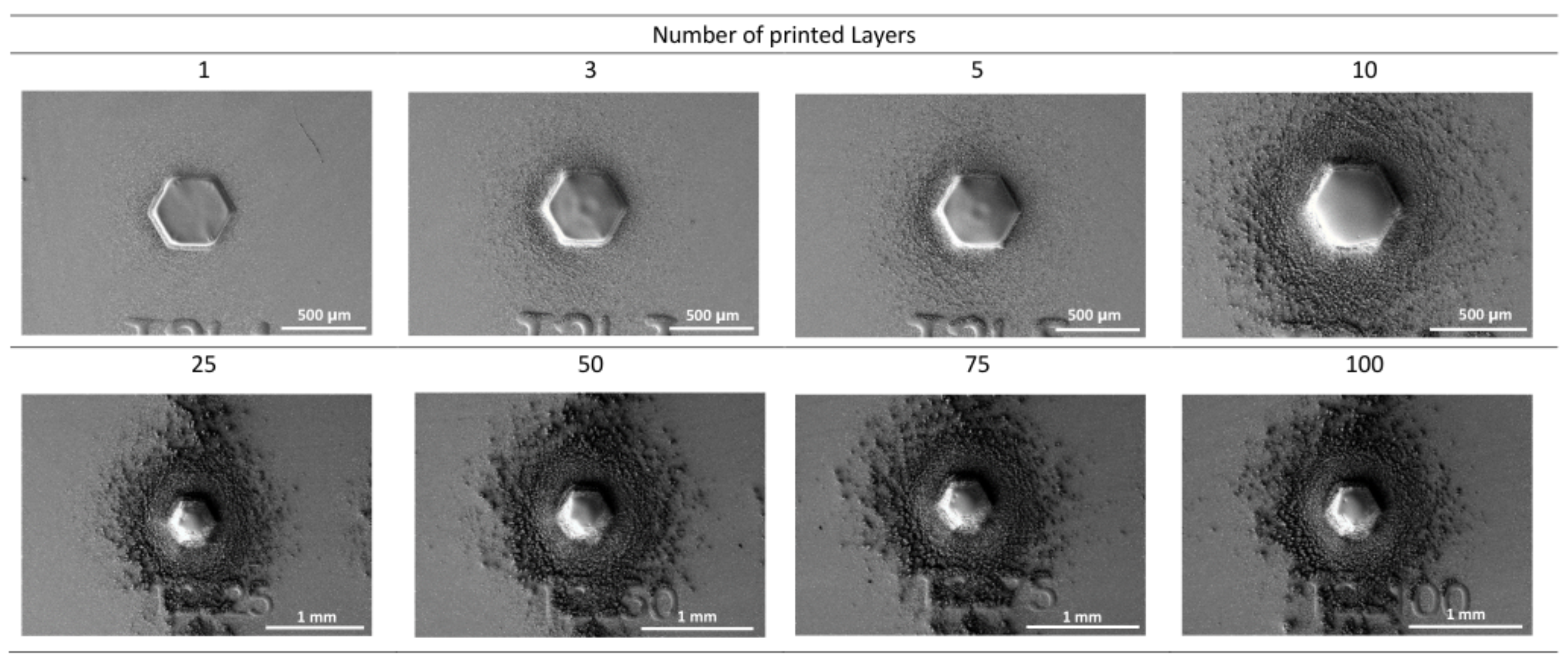
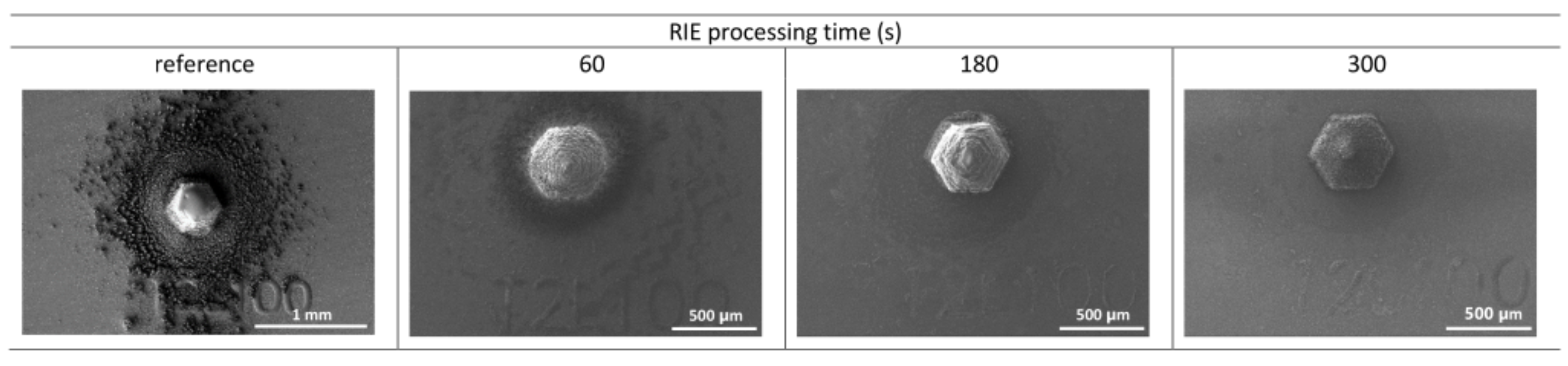
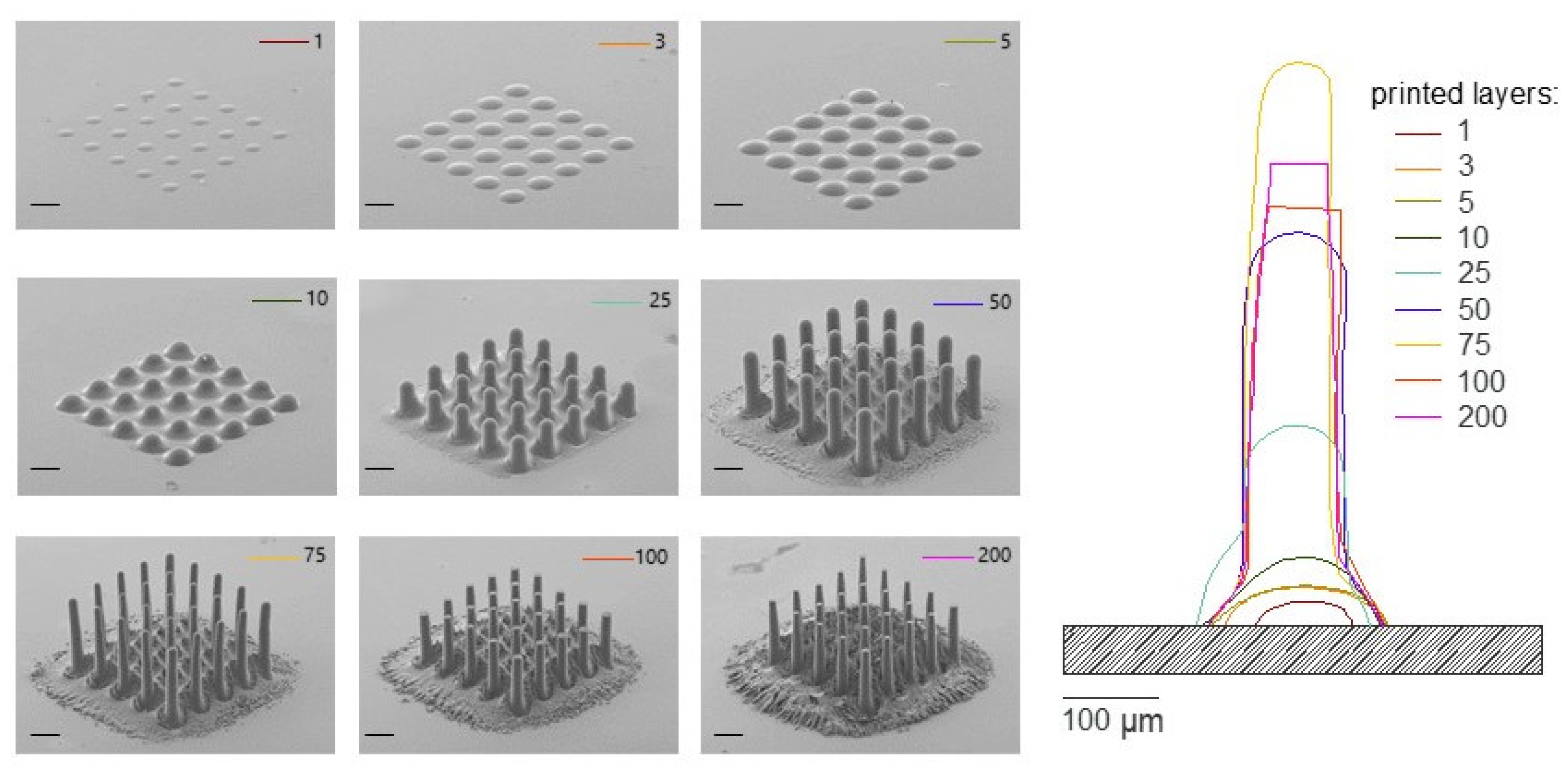
3.2. AJP Parameters Optimization
4. Conclusions
Supplementary Materials
Author Contributions
Funding
Acknowledgments
Conflicts of Interest
References
- Wilkinson, N.J.; Smith, M.A.A.; Kay, R.W.; Harris, R.A. A review of aerosol jet printing—A non-traditional hybrid process for micro-manufacturing. Int. J. Adv. Manuf. Technol. 2019, 105, 4599–4619. [Google Scholar] [CrossRef] [Green Version]
- Grunwald, I.; Groth, E.; Wirth, I.; Schumacher, J.; Maiwald, M.; Zoellmer, V.; Busse, M. Surface biofunctionalization and production of miniaturized sensor structures using aerosol printing technologies. Biofabrication 2010, 2, 14106. [Google Scholar] [CrossRef] [PubMed]
- Marquez, G.J.; Renn, M.J.; Miller, W.D. Aerosol-Based Direct-Write of Biological Materials for Biomedical Applications. MRS Online Proc. Libr. 2001, 698, 521–527. [Google Scholar] [CrossRef]
- De Silva, M.N.; Paulsen, J.; Renn, M.J.; Odde, D.J. Two-step cell patterning on planar and complex curved surfaces by precision spraying of polymers. Biotechnol. Bioeng. 2006, 93, 919–927. [Google Scholar] [CrossRef]
- Huang, Q.; Zhu, Y. Printing Conductive Nanomaterials for Flexible and Stretchable Electronics: A Review of Materials, Processes, and Applications. Adv. Mater. Technol. 2019, 4, 1800546. [Google Scholar] [CrossRef]
- Hines, D.; Gu, Y.; Martin, A.; Li, P.; Fleischer, J.; Clough-Paez, A.; Stackhouse, G.; Dasgupta, A.; Das, S. Considerations of aerosol-jet printing for the fabrication of printed hybrid electronic circuits. Addit. Manuf. 2021, 47, 102325. [Google Scholar] [CrossRef]
- Wu, W. Inorganic nanomaterials for printed electronics: A review. Nanoscale 2017, 9, 7342–7372. [Google Scholar] [CrossRef]
- Secor, E.B. Principles of aerosol jet printing. Flex. Print. Electron. 2018, 3, 35002. [Google Scholar] [CrossRef]
- Yang, H.; Rahman, M.T.; Du, D.; Panat, R.; Lin, Y. 3-D printed adjustable microelectrode arrays for electrochemical sensing and biosensing. Sens. Actuators B Chem. 2016, 230, 600–606. [Google Scholar] [CrossRef] [Green Version]
- Binder, S.; Glatthaar, M.; Rädlein, E. Analytical Investigation of Aerosol Jet Printing. Aerosol Sci. Technol. 2014, 48, 924–929. [Google Scholar] [CrossRef] [Green Version]
- Jabari, E.; Toyserkani, E. Aerosol-Jet printing of highly flexible and conductive graphene/silver patterns. Mater. Lett. 2016, 174, 40–43. [Google Scholar] [CrossRef]
- Borghetti, M.; Serpelloni, M.; Sardini, E.; Spurling, D.; Nicolosi, V. Temperature influence on Ti3C2Tx lines printed by aerosol jet printing. Sens. Actuators A Phys. 2021, 332, 113185. [Google Scholar] [CrossRef]
- Mahajan, A.; Frisbie, C.D.; Francis, L.F. Optimization of Aerosol Jet Printing for High-Resolution, High-Aspect Ratio Silver Lines. ACS Appl. Mater. Interfaces 2013, 5, 4856–4864. [Google Scholar] [CrossRef]
- Phuah, E.W.; Hart, W.L.; Sumer, H.; Stoddart, P.R. Patterning of biomaterials by aerosol jet printing: A parametric study. Bioprinting 2020, 18, e00081. [Google Scholar] [CrossRef]
- Ćatić, N.; Wells, L.; Al Nahas, K.; Smith, M.; Jing, Q.; Keyser, U.F.; Cama, J.; Kar-Narayan, S. Aerosol-jet printing facilitates the rapid prototyping of microfluidic devices with versatile geometries and precise channel functionalization. Appl. Mater. Today 2020, 19, 100618. [Google Scholar] [CrossRef]
- Chen, G.; Gu, Y.; Tsang, H.; Hines, D.R.; Das, S. The Effect of Droplet Sizes on Overspray in Aerosol-Jet Printing. Adv. Eng. Mater. 2018, 20, 1701084. [Google Scholar] [CrossRef]
- Goth, C.; Putzo, S.; Franke, J. Aerosol Jet printing on rapid prototyping materials for fine pitch electronic applications. In Proceedings of the 2011 IEEE 61st Electronic Components and Technology Conference (ECTC), Lake Buena Vista, FL, USA, 31 May–3 June 2011; pp. 1211–1216. [Google Scholar] [CrossRef]
- Seifert, T.; Sowade, E.; Roscher, F.; Wiemer, M.; Gessner, T.; Baumann, R.R. Additive Manufacturing Technologies Compared: Morphology of Deposits of Silver Ink Using Inkjet and Aerosol Jet Printing. Ind. Eng. Chem. Res. 2015, 54, 769–779. [Google Scholar] [CrossRef]
- Smith, M.; Choi, Y.S.; Boughey, C.; Kar-Narayan, S. Controlling and assessing the quality of aerosol jet printed features for large area and flexible electronics. Flex. Print. Electron. 2017, 2, 15004. [Google Scholar] [CrossRef]
- Williams, N.X.; Watson, N.; Joh, D.Y.; Chilkoti, A.; Franklin, A.D. Aerosol jet printing of biological inks by ultrasonic delivery. Biofabrication 2020, 12, 25004. [Google Scholar] [CrossRef]
- Seifert, T.; Baum, M.; Roscher, F.; Wiemer, M.; Gessner, T. Aerosol Jet Printing of Nano Particle Based Electrical Chip Interconnects. Mater. Today Proc. 2015, 2, 4262–4271. [Google Scholar] [CrossRef]
- Hester, J.; Nguyen, E.; Tice, J.; Radisic, V. A novel 3D-printing-enabled “roller coaster” transmission line. In Proceedings of the 2017 IEEE International Symposium on Antennas and Propagation USNC/URSI National Radio Science Meeting, San Diego, CA, USA, 9–14 July 2017; pp. 2639–2640. [Google Scholar] [CrossRef]
- Jing, Q.; Pace, A.; Ives, L.; Husmann, A.; Ćatić, N.; Khanduja, V.; Cama, J.; Kar-Narayan, S. Aerosol-jet-printed, conformable microfluidic force sensors. Cell Rep. Phys. Sci. 2021, 2, 100386. [Google Scholar] [CrossRef] [PubMed]
- Cao, C.; Andrews, J.B.; Franklin, A.D. Completely Printed, Flexible, Stable, and Hysteresis-Free Carbon Nanotube Thin-Film Transistors via Aerosol Jet Printing. Adv. Electron. Mater. 2017, 3, 1700057. [Google Scholar] [CrossRef]
- Rother, M.; Brohmann, M.; Yang, S.; Grimm, S.B.; Schießl, S.P.; Graf, A.; Zaumseil, J. Aerosol-Jet Printing of Polymer-Sorted (6,5) Carbon Nanotubes for Field-Effect Transistors with High Reproducibility. Adv. Electron. Mater. 2017, 3, 1700080. [Google Scholar] [CrossRef]
- Tait, J.G.; Witkowska, E.; Hirade, M.; Ke, T.H.; Malinowski, P.E.; Steudel, S.; Adachi, C.; Heremans, P. Uniform Aerosol Jet printed polymer lines with 30 μm width for 140 ppi resolution RGB organic light emitting diodes. Org. Electron. 2015, 22, 40–43. [Google Scholar] [CrossRef]
- Bag, S.; Deneault, J.R.; Durstock, M.F. Aerosol-Jet-Assisted Thin-Film Growth of CH3NH3PbI3 Perovskites—A Means to Achieve High Quality, Defect-Free Films for Efficient Solar Cells. Adv. Energy Mater. 2017, 7, 1701151. [Google Scholar] [CrossRef]
- Drew, K.; Hopman, S.; Hörteis, M.; Glunz, S.W.; Granek, F. Combining laser chemical processing and aerosol jet printing: A laboratory scale feasibility study. Prog. Photovoltaics Res. Appl. 2011, 19, 253–259. [Google Scholar] [CrossRef]
- Jabari, E.; Toyserkani, E. Micro-scale aerosol-jet printing of graphene interconnects. Carbon 2015, 91, 321–329. [Google Scholar] [CrossRef]
- Zhu, Y.; Yu, L.; Wu, D.; Lv, W.; Wang, L. A high-sensitivity graphene ammonia sensor via aerosol jet printing. Sens. Actuators Phys. 2021, 318, 112434. [Google Scholar] [CrossRef]
- Obata, K.; Klug, U.; Koch, J.; Suttmann, O.; Overmeyer, L. Hybrid Micro-stereo-lithography by Means of Aerosol Jet Printing Technology. J. Laser Micro/Nanoeng. 2014, 9, 242–247. [Google Scholar] [CrossRef] [Green Version]
- Obata, K.; Schonewille, A.; Slobin, S.; Hohnholz, A.; Unger, C.; Koch, J.; Suttmann, O.; Overmeyer, L. Hybrid 2D patterning using UV laser direct writing and aerosol jet printing of UV curable polydimethylsiloxane. Appl. Phys. Lett. 2017, 111, 121903. [Google Scholar] [CrossRef]
- Saleh, M.S.; Hu, C.; Panat, R. Three-dimensional microarchitected materials and devices using nanoparticle assembly by pointwise spatial printing. Sci. Adv. 2017, 3, e1601986. [Google Scholar] [CrossRef] [Green Version]
- Brodoceanu, D.; Bauer, C.T.; Kroner, E.; Arzt, E.; Kraus, T. Hierarchical bioinspired adhesive surfaces—A review. Bioinspiration Biomim. 2016, 11, 51001. [Google Scholar] [CrossRef]
- Vlnieska, V.; Mikhaylov, A.; Zakharova, M.; Blasco, E.; Kunka, D. Epoxy Resins for Negative Tone Photoresists. Polymers 2019, 11, 1457. [Google Scholar] [CrossRef] [PubMed] [Green Version]
- Vlnieska, V.; Zakharova, M.; Mikhaylov, A.; Kunka, D. Lithographic Performance of Aryl Epoxy Thermoset Resins as Negative Tone Photoresist for Microlithography. Polymers 2020, 12, 2359. [Google Scholar] [CrossRef] [PubMed]
- Chiamori, H.; Brown, J.; Adhiprakasha, E.; Hantsoo, E.; Straalsund, J.; Melosh, N.; Pruitt, B. Suspension of nanoparticles in SU-8: Processing and characterization of nanocomposite polymers. Microelectron. J. 2008, 39, 228–236. [Google Scholar] [CrossRef]


| Source | Variable | In This Work |
|---|---|---|
| Process | atomization gas flow sheath gas flow focus ratio aerosol flow temperature CAD design virtual impact flow | 25 SCCM a 110 SCCM a 4.422 °C 2D pillar diagram none |
| Material | solvent:solid ratio (% mol · mol) ink temperature particle size ink viscosity | cyclopentanone:aryl epoxy resin 92% 35 °C no particles 11 cP |
| Machine | printing speed stage temperature working distance nozzle diameter atomizer type ultrasonic current | 3 mm· s−1 75 °C 4.7 mm 200 μm ultrasonic 500 mA |
Publisher’s Note: MDPI stays neutral with regard to jurisdictional claims in published maps and institutional affiliations. |
© 2022 by the authors. Licensee MDPI, Basel, Switzerland. This article is an open access article distributed under the terms and conditions of the Creative Commons Attribution (CC BY) license (https://creativecommons.org/licenses/by/4.0/).
Share and Cite
Vlnieska, V.; Gilshtein, E.; Kunka, D.; Heier, J.; Romanyuk, Y.E. Aerosol Jet Printing of 3D Pillar Arrays from Photopolymer Ink. Polymers 2022, 14, 3411. https://doi.org/10.3390/polym14163411
Vlnieska V, Gilshtein E, Kunka D, Heier J, Romanyuk YE. Aerosol Jet Printing of 3D Pillar Arrays from Photopolymer Ink. Polymers. 2022; 14(16):3411. https://doi.org/10.3390/polym14163411
Chicago/Turabian StyleVlnieska, Vitor, Evgeniia Gilshtein, Danays Kunka, Jakob Heier, and Yaroslav E. Romanyuk. 2022. "Aerosol Jet Printing of 3D Pillar Arrays from Photopolymer Ink" Polymers 14, no. 16: 3411. https://doi.org/10.3390/polym14163411
APA StyleVlnieska, V., Gilshtein, E., Kunka, D., Heier, J., & Romanyuk, Y. E. (2022). Aerosol Jet Printing of 3D Pillar Arrays from Photopolymer Ink. Polymers, 14(16), 3411. https://doi.org/10.3390/polym14163411