Abstract
Electronic and magnetic properties of Ga14N16−nGd2Cn monolayers are investigated by means of the first principle calculation. The generalized gradient approximation (GGA) of the density functional theory with the on-site Coulomb energy U was considered (GGA + U). It is found that the total magnetic moment of a Ga14N16Gd2 monolayer is 14 with an antiferromagnetic (AFM) phase. C atom substitutional impurity can effectively change the magnetic state of Ga14N16−nGd2Cn monolayers to ferromagnetic phases (FM), and the magnetic moment increases by 1/1C. The stable FM phase is due to the p-d coupling orbitals between the C-2p and Gd-5d states. Moreover, Curie temperature (TC) close to room temperature (TR, 300 K) is observed in the Ga14N16Gd2C2 monolayer, and the highest value can reach 261.46 K. In addition, the strain effect has a significant positive effect on the of the Ga14N16−nGd2Cn monolayer, which is much higher than the , and the highest value is 525.50 K. This provides an opportunity to further explore the application of two-dimensional magnetic materials in spintronic devices.
1. Introduction
Diluted magnetic semiconductors (DMSs), as an important part of spintronics, have attracted much attention in terms of harnessing the spin and charge of electrons [1,2,3]. Scientists modulate the ferromagnetism and by controlling the doping atoms to investigate the potential applications of DMSs. It opens a new gateway for extending future classes of materials. A magnetic dopant was used to substitute cations in the host compound semiconductors and observed distinct properties [4,5,6]. The room-temperature FM (-FM) phase has been observed in Cr, Mn, Fe, Co-doped TiO2, ZnO and GaN [7,8,9].
The metal nitrides (MNs), including group IIIA nitrides and nitride MXene, exhibit unique electronic and magnetic characteristics [10,11,12]. In recent decades, scientists have paid much attention to the magnetic properties and of GaN materials doped with transition metal (TM) [13,14,15], alkali metal, alkaline earth metal, etc. [16,17,18]. The low solubility of TM atoms in GaN materials restrains their potential application in -FM spintronic devices. In addition, rare-earth elements such as Sm, Dy and Gd with large magnetic moments have attracted a lot of attention [19,20,21]. Nobuaki found that the TC of GaN:Gd materials achieves a of 400 K, far above [22]. The -FM coupling of the GaN:Gd system was also detected by Asahi [23]. Dhar’s group found a colossal magnetic moment and -FM phase at a low concentration of Gd atoms [24,25]. It is well known that defects are one of the important reasons for FM and AFM coupling in GaN-based systems. The spintronic properties of GaN-based materials can be modulated not only by n-type (interstitial O, N and C dopants) but also by p-type defects (Ga vacancies and transition metal doping) [26,27,28,29]. Dalpian found that the FM phase in n-type GaN is mainly derived from s-f orbital hybridization [30]. It was found that the 4f orbitals of Gd are usually far from the Fermi energy [31]. Therefore, the s-f coupling effect near the Fermi energy level will be weak. Xie found -FM in the GaN:Gd nanowires doped with C atoms, which are strongly influenced by hybridized p-d coupling [32]. Therefore, it is necessary to select a suitable material doped with GaN:Gd and to explore the origin of the ferromagnetic mechanism in-depth and definitively.
Until now, there has been a lot of research, but the research on GaN:Gd monolayers doped with C atoms is sparse. In the presented paper, the electronic and magnetic properties of Gd-pair-doped GaN () monolayers with and without C atoms are studied by employing the first principle calculation. This paper is organized as follows. In Section 2, we present the details of computational methods. In Section 3.1, the geometric structure, band structure, partial density of states (PDOS), magnetic properties and of monolayers doped with and without C atoms are determined. In Section 3.2, the biaxial strain effect in Ga14N16−nGd2Cn monolayers are investigated. In Section 4, the results are briefly concluded.
2. Computational Method
All calculations are based on the density function theory (DFT) of the exchange-correlation potential. The computational work is conducted by using Vienna ab initio simulation packages (VASP) [33]. The Perdew–Burke–Ernzerhof (PBE) formalism of the generalized gradient approximation (GGA) is used to deal with electron exchange and correlation energies by using projection-enhanced waves (PAW) to understand the interactions between electrons and ions [34]. The cutoff energy of the plane wave basis set is kept at 500 eV [16]. When the structure is optimized, the atomic force and the energy convergence are kept at 0.01 eV/Å and 10−5 eV [13], respectively. A vacuum space above 12 Å is created to eliminate the effects of interactions between neighboring layers along the z-direction. The sample of k points in the Brillouin zone is set as 5 × 5 × 1 [3]. The valence electron configurations of Ga, N, Gd and C atoms are described as: , respectively. A self-consistent formulation of on-site Coulomb interaction for the Gd-4f orbitals is computed. The Coulomb repulsion energy U and the exchange parameter J are set to 6.7 eV and 0.7 eV, respectively [30,31].
The structural stability is studied by the binding energy (), which is expressed as [35]:
where represents the total energy of Ga14N16−nGd2Cn, , , and corresponding to the energy of isolated Ga, N, Gd and C atoms, respectively.
We performed calculations of critical temperature to fully characterize the magnetic properties of monolayers. The Heisenberg model based on the mean-field approximation theory is used to estimate the [16]:
where KB and n are the Boltzmann constant and the number of Gd atoms, respectively. This temperature is often overestimated by the mean field approximation, thus an empirical relationship is used [36]:
3. Results and Discussion
The top and side views of atomic structures of free-standing GaN monolayers () are relaxed to a flat honeycomb structure which is stripped from the (0001) plane of wurtzite GaN structure. The band structure and PDOS of the pure GaN monolayer in Figure S1a,e (shown in Supplementary Materials) indicate that the spin-up and spin-down channels are degenerated, indicating a non-magnetic semiconductor material. It possesses a wide band gap of 2.32 eV with a Ga-N bond length of about 1.84 Å, which agrees with previous studies [35,37,38]. Figure 1a,b shows the top and side views of optimized monolayers. The bulges in the doping position show that the Gd atom have tendency to break away from the monolayer. It is also shown in Figure S1 and Table S1 that different concentrations of Gd have a weak effect on the electronic structure and magnetic properties of the GaN:Gd monolayer. Thus, monolayers are used as the main research subject. The substitution sites have a great influence on the monolayer, so we explored the effects of different doping sites on the electronic properties, magnetic properties and (the details are placed in Table S1, Figures S2 and S3). The topic of this article revolves around the optimal structures, with doping sites (M), (M, 8) and (M, 5, 7), respectively.
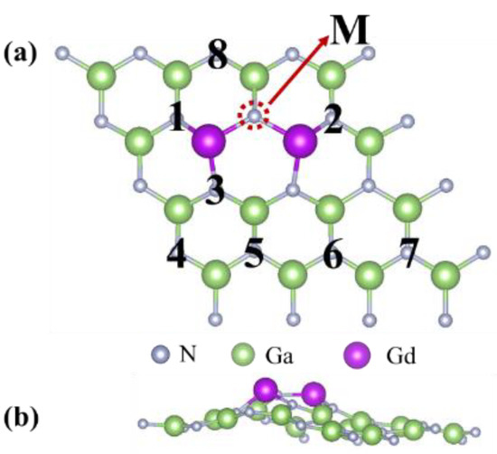
Figure 1.
(a) Top and (b) side views of the optimized structures of monolayers.
3.1. The Structural, Magnetic Properties and TC
The charge density differences of Ga14N16−nGd2Cn monolayers are depicted in Figure 2, which is used to effectively investigate the accumulation and depletion of electrons. It is defined as: , where , and represent the total charge density of the Ga14N16−nGd2Cn monolayer, the pure monolayer and the free standing Gd and C atoms, respectively. The yellow region represents the accumulation of electrons, whereas the cyan region represents the depletion of electrons. The yellow region is mainly located in N and C atoms, whereas the cyan region is mainly shown in Gd atoms. The above phenomenon is noticeable in the doped atoms and adjacent atomic positions. It is suggested that electrons in Gd and Ga atoms are depleted and transferred to N and C atoms.
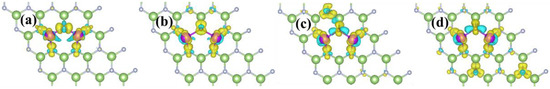
Figure 2.
The charge density difference of (a) , (b) , (c) and (d) monolayers. The isosurface level is 0.009 . The yellow and cyan areas indicate the positive and negative electrons, respectively.
To clearly and quantitatively describe the electron transfer characters, the Bader analysis is established in Table 1. As in the above analysis, electrons depleted on Ga and Gd atoms and accumulated on N and C atoms. In monolayers, it is found that the Ga atoms lose about 1.35|e|, the N atoms bonded without Gd atoms gain about 1.37|e| and the N atoms bonded with Gd atoms gain 1.47|e|, which is 7.30% more than the former. Each Gd atom loses about 1.85|e| and the introduction of C atoms has a negligible effect on this. The M site is special and is located between the two Gd atoms. The electron of N atoms at this position is 1.58|e|, 15.33% more than that of other N atoms. When the C atom replaces this position, the obtained electron is 1.35|e|, which becomes the same as the N atom bonded without Gd atoms, and no longer maintains specificity. The Ga atom bonded with C loses 1.24|e|, which is reduced 7.46%.

Table 1.
Calculated Bader analysis for Ga, N, Gd and C (except for M site) atoms, respectively. The M site is located between the two Gd atoms. and represent the Ga atom bonded with and without C, respectively, whereas and display the N atoms bonded with and without Gd atoms, respectively. The accumulation and depletion of electrons are indicated by + and −, respectively. The unit of all data is |e|.
Figure 3a–f depicts the energy band structures of Ga14N16−nGd2Cn monolayers without considering spin–orbital coupling (SOC). In monolayers (shown in Figure S1b), the conduction band minimum (CBM) is located at the Γ point along the high symmetry in the first Brillouin zone (BZ), whereas the valence band maximum (VBM) is located at K points. It can be seen from the energy band diagram, where the CBM maintains its original state, whereas the VBM rises slightly due to the orange energy level contributed by the C atom. The band gaps of the spin-up channels are 1.99 eV, 1.83 eV, 1.93 eV and 1.93 eV, respectively, whereas the spin-down channels are 2.05 eV, 0.56 eV, 0.74 eV and 0.46 eV, respectively. The band gap sharply decreased in the spin-down channel. This phenomenon is a consequence of the introduction of impurity energy levels near the Fermi energy level, which originates from the C atom. It can be seen that the C atom can transform the GaN:Gd monolayer into a spin-polarized semi-metal-like unique property with the spin-up channel maintaining a wide band gap and the spin-down channel having a small band gap.
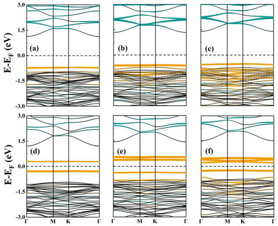
Figure 3.
The spin-up band structures of (a) , (b) and (c) monolayers. The spin-down channels of (d) , (e) and (f) monolayers. The green and orange dotted lines represent the energy levels of Gd and C atoms, respectively. The dashed lines represent the Fermi level, which is taken to be 0.
The total magnetic moments of are 14.00 , 15.00 , 16.00 and 17.00 , respectively. In Table 2, the spin details are depicted. For the monolayer, the magnetic moment is entirely contributed to by the Gd atoms. With an increasing number of C atoms, the ratios are reduced to 94.53%, 89.50% and 84.24%, respectively. Each C atom substitutes an N atom resulting in a hole, which is the reason for the increase in the magnetic moment by 1 . It is also shown that the increases significantly under the influence of C atoms, with values of 58.22 K, 428.63 K and 319.32 K, respectively. A stable FM phase with a high magnetic moment and the highest is obtained in the monolayer. It is amended as 35.51 K, 264.46 K and 194.78 K, respectively. By comparing previous studies (shown in Table S2), Gd atoms in monolayers can introduce large magnetic moments, and the introduction of C atoms can further increase the magnetic moments.
Table 2.
Magnetic moments (), energy difference (, meV), nearest-neighboring exchange coupling (J/eV) and estimated Curie temperature (/K) of monolayers, respectively.
To further investigate the magnetic mechanism, the PDOSs of Ga14N16−nGd2Cn monolayers are plotted in Figure 4. It is further identified that the large magnetic moment stems mainly from the large exchange splitting of the Gd-4f state. The spin-up Gd-4f orbitals (below the VBM) are fully occupied while the spin-down orbitals (above the CBM) are fully unoccupied. The CBM is pushed to the Γ-point (shown in Figure 3) in the spin-down channel and decreases the electron effective mass which agrees with the previous report [39]. The Gd-4f orbitals are separated from the VBM (in the spin-up channel) and the CBM (in the spin-down channel) by about 4 and 7 eV, respectively. As a result, the coupling between Gd-4f and p-type orbitals should be weak [31]. In the spin-down channel, in agreement with the energy band analysis above, the C atom impurity energy level appears near the Fermi energy level and the CBM is reduced, leading to a small band gap. The Gd-5d orbitals and C-2p orbitals overlap near the Fermi energy level, forming p-d hybrid orbitals, and the C-2p near the Fermi energy level is significantly enhanced as the concentration of C atoms increases. Thus, we suggest that the stable FM phase originates from p-d hybridized orbitals.
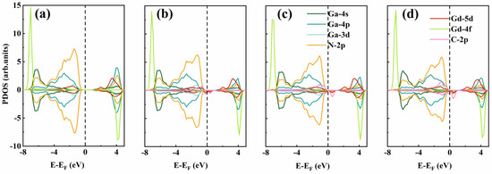
Figure 4.
Spin-polarized partial density of states (PDOS) of (a) , (b) , (c) and (d) monolayers, respectively. The dashed lines represent the Fermi level which is taken to be 0.
3.2. The Modulation by Strain Effect
The biaxial strains () ranging from −6% to 15% are performed on monolayers. The total energy () and of FM states are shown in Figure 5a,b, which is used to review the stability. The negative Eb indicates an exothermic reaction, and the larger |Eb| means a more stable structure. The structural stability decreases as the curve decreases, whereas a rising one means that it is more stable. It can be clearly seen that structural stability decreases with increasing compressive strain. As the tensile strain increases, the stability of the system first increases, reaching a maximum at ε = 2, and then exhibits a significant decrease. Figure 5c shows the impact of strain effects on the band gap of the system. It can be seen that the compression strain has a nominal impact on the spin-up channel indicated by the solid line. For the spin-up band gap, similar trends exist for the total energy and . Although the spin-down band gap shows slight fluctuations at −4 ≤ ε ≤ 12, the value decreases significantly when ε ≤ −5 or ε ≥ 13.
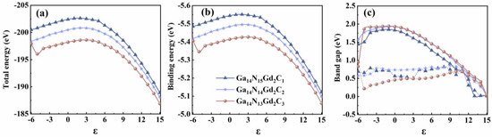
Figure 5.
(a) of FM phase, (b) and (c) band gap of Ga14N16−nGd2Cn monolayers. The dark blue (triangle), light blue (pentagram) and brown (circle) lines in the diagram represent monolayers, respectively.
and J are shown in Figure 6a,b and are used as criteria for the magnetic characters and predicting the evolution of the . Positive and increasing values represent a stronger stable FM state. At −4 < ε < 15, the strain effect does not change the magnetic ground state of , and the ground states of all structures are the FM states. When ε ≤ −5, possesses negative values, implying that the ground state is AFM. Additionally, the maximum values of for are obtained as 125.4 eV (ε = −4), 242.87 eV (ε = 7) and 125.91 eV (ε = −3), respectively. The can be predicted to reach a maximum. Figure 6c,d demonstrates the and whose value increased to above with strain effects. The highest () is found for as 295.89 K (485.07 K, ε = −4), 564.57 K (925.53 K, ε = 7) and 297.09 K (487.04 K, ε = −3), respectively. It is clearly noticeable from the graph that the curve is most stable when n = 2, with fluctuating around 300 K under strain effects.
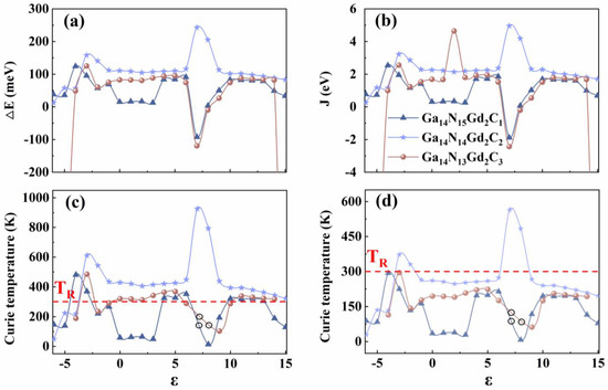
Figure 6.
(a) Energy difference (△E), (b) the magnetic coupling parameter (J), (c) and (d) . The dark blue (triangle), light blue (pentagram) and brown (circle) lines in the diagram represent the monolayers, respectively. The red dashed lines in the last two graphs indicate . The black circles in the last two figures indicate this position as an AFM state without .
The strains acting in the monolayer of ε = −6, 7 and 15 are used as an example to understand the mechanism of orbital hybridization that causes the change, whose PDOS is plotted in Figure 7. As can be seen in Figure 7b, the Gd-5d states and C-2p states overlap a lot near the Fermi energy, which indicates the coupling between them and the formatting of p-d orbitals. This is consistent with the results discussed above. A weakening of this coupling is found in Figure 7a,c, which is due to a reduction in the Gd-5d electronic state near the Fermi energy level, resulting in a reduction in . In addition, the results obtained from the above analysis are further verified by the SOC method (shown in Figure S4). In conclusion, the replacement of N atoms with C atoms effectively transforms the GaN:Gd monolayer into a stable FM phase, which is further processed by biaxial strain to obtain GaN-based materials close to or even well above .
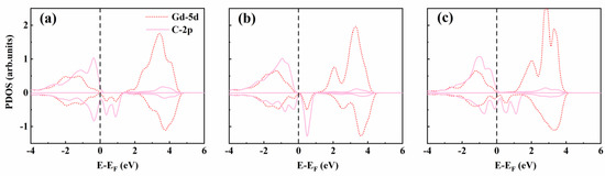
Figure 7.
The PDOS of monolayers at ε = (a) 6, (b) 7 and (c) 15, respectively.
4. Conclusions
In conclusion, the electronic and magnetic properties of Ga14N16−nGd2Cn monolayers are studied by means of the DFT method. The total magnetic moment of the monolayer is 14 with a weak AFM phase. The magnetic moment stems mainly from the large exchange splitting of the Gd-4f state. It is suggested that the magnetic moment of the monolayer, in which the N atom has been substituted with a C atom, is increased with a stable FM phase. The main contributing factor is the hybridized p-d orbital between the Gd-5d and C-2p orbitals. A relatively high of 261.46 K is observed in the monolayers. In addition, the FM coupling and can be further enhanced by suitable strain effects. The of the monolayer can be significantly increased to 564.57 K, well above .
Supplementary Materials
The following supporting information can be downloaded at: https://www.mdpi.com/article/10.3390/cryst13030531/s1, Figure S1: Band structures of (a) (b), (c) and (d) monolayers. The blue and pink solid lines in the band structure represent spin up and spin down channels, respectively. PDOS of (e) (f), (g) and (h) monolayers. The dash lines present the fermi-level which is taken to be 0.; Table S1: The of FM phase, total magnetic moments (), ), nearest-neighboring exchange (J), estimated and of , respectively. Figure S2: PDOS with FM states of different substitution site: [1], [4], [M, 2], [5, 7], [2, M, 5] and [1, M, 2]. Figure S3: PDOS with AFM states of different substitution site: [1], [4], [M, 2], [5, 7], [2, M, 5] and [1, M, 2]. Figure S4: (a) of FM phase, (b) , (c) △E (d) J, (e) and (f) of Ga14N16−nGd2Cn monolayers computed by the PBE method with SOC. The dark blue (triangle), light blue (pentagram) and brown (circle) lines in the diagram represent monolayers, respectively. The black circles in the last two figures indicate this position as an AFM state without . Table S2: A brief summary of the magnetic properties for doped GaN materials. References [40,41,42,43,44] are cited in Supplementary Materials.
Author Contributions
Conceptualization, S.T. and H.X.; methodology, S.L., L.H. and S.T.; software, Y.H., H.X. and X.C.; validation, L.Z., Y.L. and H.X.; formal analysis, S.T.; investigation, S.T.; resources, S.T.; data curation, S.T.; writing—original draft prep-aration, S.T.; writing—review and editing, L.Z., H.X. and X.C.; visualization, Y.L., A.L. and H.X.; supervision, Y.L., A.L. and H.X.; project administration, H.X.; Supervision, R.X. All authors have read and agreed to the published version of the manuscript.
Funding
This research received no external funding.
Data Availability Statement
All data that support the findings of this study are included within the article (and Supplementary Files).
Acknowledgments
The authors would like to acknowledge the financial support from the Fundamental Research Funds for the Central Universities (2232022A-11), the Fundamental Research Funds for the Central Universities and Graduate Student Innovation Fund of Donghua University (CUSF-DH-D-2022074) and the computational support from the Shanghai Supercomputer Center of the National Natural Science Foundation of Shanghai (21ZR1402200).
Conflicts of Interest
The authors declare no conflict of interest.
References
- Wolf, S.A.; Awschalom, D.D.; Buhrman, R.A.; Daughton, J.M.; von Molnár, S.; Roukes, M.L.; Chtchelkanova, A.Y.; Treger, D.M. Spintronics: A Spin-Based Electronics Vision for the Future. Science 2001, 294, 1488–1495. [Google Scholar] [CrossRef]
- Sato, K.; Katayama, Y. First principles materials design for semiconductor spintronics. Semicond. Sci. Technol. 2002, 17, 367–376. [Google Scholar] [CrossRef]
- Zhao, Q.; Xiong, Z.; Luo, L.; Sun, Z.H.; Qin, Z.Z.; Chen, L.L.; Wung, N. Design of a new two-dimensional diluted magnetic semiconductor: Mn-doped GaN monolayer. Appl. Surf. Sci. 2017, 396, 480. [Google Scholar] [CrossRef]
- Dietl, T.; Ohno, H.; Matsukura, F.; Cibert, J.; Ferrand, D. Zener Model Description of Ferromagnetism in Zinc-Blende Magnetic Semiconductors. Science 2000, 287, 1019–1022. [Google Scholar] [CrossRef]
- Esch, A.V.; Bockstal, L.V.; Boeck, J.D.; Verbanck, G.; Steenbergen, A.S.V.; Wellmann, P.J.; Grietens, B.; Bogaerts, R.; Herlach, F.; Borghs, G. Interplay between the magnetic and transport properties in the III–V diluted magnetic semiconductor Ga1−xMnxAs. Phys. Rev. B 1997, 56, 7392–7394. [Google Scholar]
- Munekata, H.; Ohno, H.; Molnar, S.V.; Segmüller, A.; Chang, L.L.; Esaki, L. Diluted magnetic III-V semiconductors. Phys. Rev. Lett. 1989, 63, 1849–1852. [Google Scholar] [CrossRef]
- Matsumoto, Y.J.; Murakami, M.; Shono, T.; Hasegawa, T.; Fukumura, T.; Kasawaki, M.; Ahmet, P.; Chiyow, T.; Koshihara, S.Y.; Koinuma, H. Room temperature ferromagnetism in transparent transition metal-doped titanium dioxide. Science 2001, 291, 854–856. [Google Scholar] [CrossRef]
- Neal, J.R.; Behan, A.J.; Ibrahim, R.M.; Blythe, H.J.; Ziese, M.; Fox, A.M.; Gehring, G.A. Room temperature magneto-optics of ferromagnetic transition-metal-doped ZnO thin films. Phys. Rev. Lett. 2006, 96, 197208. [Google Scholar] [CrossRef] [PubMed]
- Lee, J.S.; Lim, J.D.; Khim, Z.G.; Park, Y.D. Magnetic and structural properties of Co, Cr, V ion-implanted GaN. J. Appl. Phys. 2003, 93, 4512–4516. [Google Scholar] [CrossRef]
- Du, K.; Xiong, Z.H.; Ao, L.; Chen, L.L. Tuning the electronic and optical properties of two-dimensional gallium nitride by chemical functionalization. Vauum 2021, 185, 110008. [Google Scholar] [CrossRef]
- Zheng, F.F.; Xiao, X.; Xie, J.; Zhou, L.J.; Li, Y.Y.; Dong, H.L. Structures, properties and applications of two-dimensional metal nitrides: From nitride MXene to other metal nitrides. 2D Mater. 2022, 9, 022001. [Google Scholar] [CrossRef]
- Alaal, N.; Roqan, I.S. Tuning the electronic properties of hexagonal teo-demensional GaN monolayers via doping for enhanced optoelectronic applications. ACS Appl. Nano Mater. 2019, 2, 202–213. [Google Scholar] [CrossRef]
- Chen, G.X.; Li, H.F.; Yang, X.; Wen, J.Q.; Pang, Q.; Zhang, J.M. Adsorption of 3d transition metal atoms on graphene-like gallium nitride monolayer: A first-principles study. Superlattices Microstruct. 2018, 115, 108–115. [Google Scholar] [CrossRef]
- Hussain, F.; Cai, Y.Q.; Khan, M.J.I.; Imran, M.; Rashid, M.; Ullah, H.; Ahmad, E.; Kousar, F.; Ahmad, S.A. Enhanced ferromagnetic properties of Cu doped two-dimensional GaN mono-layer. Int. J. Mod. Phys. C 2015, 26, 1550009. [Google Scholar] [CrossRef]
- Li, J.; Liu, H. Magnetism investigation of GaN monolayer doped with group VIII B transition metals. J. Mater. Sci. 2018, 53, 15986–15994. [Google Scholar] [CrossRef]
- Chen, G.X.; Fan, X.B.; Li, S.Q.; Zhang, J.M. First-principles study of magnetic properties of alkali metals and alkaline earth metals doped two-dimensional GaN materials. Acta Phys. Sin. 2019, 68, 237303. [Google Scholar] [CrossRef]
- Gutiérrez, C.A.H.; Moreno, Y.L.C.; Kuoppa, V.T.R.; Cardona, D.; Hu, Y.Q.; Kudriatsev, Y.; Serrano, M.A.Z.; Hernandez, S.G.; Lopez, M.L. Study of the heavily p-type doping of cubic GaN with Mg. Sci. Rep. 2020, 10, 16858. [Google Scholar] [CrossRef] [PubMed]
- Yeoh, K.H.; Yoon, T.L.; Lim, T.L.; Rusi; Ong, D.S. Monolayer GaN functionalized with alkali metal and alkaline earth metal atoms: A first-principles study. Superlattices Microstruct. 2019, 130, 428–436. [Google Scholar] [CrossRef]
- Li, Y.; Xie, X.J.; Liu, H.; Wang, S.; Hao, Q.Y.; Liang, L.M.; Liu, C.C. Effect of carbon on the magnetic properties of Dy-implanted GaN films. J. Alloys Compd. 2018, 762, 887–891. [Google Scholar] [CrossRef]
- Maskar, E.; Lamrani, A.F.; Belaiche, M.; Smairi, A.E.; Vu, T.V.; Rai, D.P. A DFT study of electronic, magnetic, optical and transport properties of rare earth element (Gd, Sm)-doped GaN material. Mater. Sci. Semicond. Process. 2022, 139, 106326. [Google Scholar] [CrossRef]
- Maekawa, M.; Miyashita, A.; Sakai, S.; Kawasuso, A. Gadolinium-implanted GaN studied by spin-polarized position annihilation spectroscopy. Phys. Rev. B 2020, 102, 05442. [Google Scholar] [CrossRef]
- Nobuaki, T.; Suzuki, A.; Yasushi, N.; Kawasuso, A. Room-temperature observation of ferromagnetism in diluted magnetic semiconductor GaGdN grown by RF-molecular beam epitaxy. Solid State Commun. 2002, 122, 651–653. [Google Scholar]
- Asahi, H.; Zhou, Y.K.; Hashimoto, M.; Kim, M.S.; Li, X.J.; Emura, S.; Hasegawa, S. GaN-based magnetic semiconductors for nanospintronics. J. Phys. Condens. Matter 2004, 16, S555. [Google Scholar] [CrossRef]
- Dhar, S.; Brandt, O.; Ramsteiner, M.; Kim, M.S.; Emura, S.; Hasegawa, S. Colossal magnetic moment of Gd in GaN. Phys. Rev. Lett. 2005, 94, 037205. [Google Scholar] [CrossRef]
- Dhar, S.; Kammermeier, T.; Ney, A. Ferromagnetism and colossal magnetic moment in Gd-focused ion-beam-implanted GaN. Appl. Phys. Lett. 2006, 89, 06250. [Google Scholar] [CrossRef]
- Liu, Z.Q.; Yi, X.Y.; Wang, J.W.; Kang, J.; Melton, A.G.; Shi, Y.; Lu, N.; Wang, J.X.; Li, J.M.; Ferguson, L. Ferromagnetism and its stability in n-type Gd-doped GaN: First-principles calculation. Appl. Phys. Lett. 2012, 100, 232408. [Google Scholar] [CrossRef]
- Mitra, C.; Lambrecht, W.R.L. Interstitial-nitrogen- and oxygen-induced magnetism in Gd-doped GaN. Phys. Rev. B 2009, 80, 081202. [Google Scholar] [CrossRef]
- Xie, R.K.; Xing, H.Z.; Zeng, Y.J.; Huang, Y.; Lu, A.J.; Chen, X.S. Room temperature ferromagnetism in Cu–Gd co-doped GaN nanowires: A first-principles study. Phys. Lett. A 2019, 383, 54–57. [Google Scholar] [CrossRef]
- Thiess, A.; Blügel, S.; Dederichs, P.H.; Zeller, R.; Lambrecht, W.R.L. Systematic study of the exchange interactions in Gd-doped GaN containing N interstitials, O interstitials, or Ga vacancies. Phys. Rev. B 2015, 92, 100418. [Google Scholar] [CrossRef]
- Dalpian, G.M.; Wei, S.H. Electron-induced stabilization of ferromagnetism in Ga1−xGdxN. Phys. Rev. B 2005, 72, 115201. [Google Scholar] [CrossRef]
- Liu, L.; Yu, P.Y.; Ma, Z.X.; Mao, S.S. Ferromagnetism in GaN:Gd: A density functional theory study. Phys. Rev. Lett. 2008, 100, 127203. [Google Scholar] [CrossRef]
- Xie, R.K.; Xing, H.Z.; Zeng, Y.J.; Liang, Y.; Chen, S.X. First-principles calculations of GaN:Gd nanowires: Carbon-dopants-induced room-temperature ferromagnetism. AIP Adv. 2017, 7, 115003. [Google Scholar] [CrossRef]
- Kresse, G.; Furthmuller, J. Efficiency of ab-initio total energy calculations for metals and semiconductors using a plane-wave basis set. Comp. Mater. Sci. 1996, 6, 15–50. [Google Scholar] [CrossRef]
- Perdew, J.P.; Burke, K.; Ernzerho, M. Generalized Gradient Approximation Made Simple. Phys. Rev. Lett. 1996, 77, 3865–3868. [Google Scholar] [CrossRef] [PubMed]
- Li, S.; Lu, A.J.; Xie, R.K.; Xing, H.Z.; Zeng, Y.J.; Huang, Y.; Chen, X.S. Tunable electronic and magnetic properties of functionalized (H, Cl, OH) germanium carbide Sheet. J. Nanosci. Nanotechnol. 2017, 17, 3927–3933. [Google Scholar] [CrossRef]
- Lin, X.; Mao, Z.; Dong, S.G.; Jian, X.D.; Han, R.; Wu, P. First-principles study on the electronic structures and magnetic properties of TM-doped (TM = V, Cr, Mn, and Fe) tetragonal ScN monolayer. J. Magn. Magn. Mater. 2021, 527, 167764. [Google Scholar] [CrossRef]
- Şahin, H.; Cahangirov, S.; Topsakal, M.; Bekaroglu, E.; Akturk, E.; Senger, R.T.; Ciraci, S. Monolayer honeycomb structures of group-IV elements and III-V binary compounds: First-principles calculations. Phys. Rev. B 2009, 80, 155453. [Google Scholar] [CrossRef]
- Ranchal, R.; Yadav, B.S.; Trampert, A. Ferromagnetism at room temperature of c- and m-plane GaN: Gd films grown on different substrates by reactive molecular beam epitaxy. J. Phys. D Appl. Phys. 2013, 46, 075003. [Google Scholar] [CrossRef]
- Liechtenstein, A.I.; Katsnelson, M.I.; Antropov, V.P.; Gubanov, V.A. Local spin density functional approach to the theory of exchange interactions inferromagnetic metals and allys. J. Magn. Magn. Mater. 1987, 67, 65–74. [Google Scholar] [CrossRef]
- Zhang, Z.W.; Shang, J.Z.; Jiang, C.Y.; Rasmita, A.; Gao, W.B.; Wu, T. Direct photoluminescence probing of ferromagnetism in monolayer two-dimensional CrBr3. Nano Lett. 2019, 19, 3138–3142. [Google Scholar] [CrossRef]
- Huang, B.; Clark, G.; Moratalla, E.N.; Klein, D.R.; Cheng, R.; Seyler, K.L.; Zhong, D.; Schmidgall, E.; Mcguire, M.A.; Cobden, D.H.; et al. Layer-dependent ferromagnetism in a Van der Waals crystal down to the monolayer limit. Nature 2017, 546, 270–273. [Google Scholar] [CrossRef]
- Deng, Y.J.; Yu, Y.J.; Song, Y.C.; Zhang, J.Z.; Wang, N.Z.; Sun, Z.Y.; Yi, Y.F.; Wu, Y.Z.; Wu, S.W.; Zhu, J.Y.; et al. Gata-tunable room-temperature ferromagnetism in two-dimensional Fe3GeTe2. Nature 2018, 563, 94–99. [Google Scholar] [CrossRef]
- Li, B.; Wan, Z.; Wang, C.; Chen, P.; Huang, B.; Cheng, X.; Qian, Q.; Li, J.; Zhang, Z.W.; Sun, G.Z.; et al. Van der Waals epitaxial growth of air-stable CrSe2 nanosheets with thickness-tunable magnetic order. Nat. Mater. 2021, 20, 818–825. [Google Scholar] [CrossRef]
- Gong, C.; Li, L.; Li, Z.L.; Ji, H.W.; Stern, A.; Xia, Y.; Cao, T.; Bao, W.; Wang, C.Z.; Wang, Y.; et al. Discovery of intrinsic ferromagnetism in two-dimensional Van der Waals crystals. Nature 2017, 546, 265–269. [Google Scholar] [CrossRef]
Disclaimer/Publisher’s Note: The statements, opinions and data contained in all publications are solely those of the individual author(s) and contributor(s) and not of MDPI and/or the editor(s). MDPI and/or the editor(s) disclaim responsibility for any injury to people or property resulting from any ideas, methods, instructions or products referred to in the content. |
© 2023 by the authors. Licensee MDPI, Basel, Switzerland. This article is an open access article distributed under the terms and conditions of the Creative Commons Attribution (CC BY) license (https://creativecommons.org/licenses/by/4.0/).