Abstract
Germanium films were grown on c-plane sapphire with a 10 nm AlAs buffer layer using molecular beam epitaxy. The effects of Ge film thickness on the surface morphology and crystal structure were investigated using ex situ characterization techniques. The nucleation of Ge proceeds by forming (111) oriented three-dimensional islands with two rotational twin domains about the growth axis. The boundaries between the twin grains are the origin of the 0.2% strain and tilt grains. The transition to a single-grain orientation reduces the strain and results in a better-quality Ge buffer. Understanding the role of thickness on material quality during the Ge(111)/Al2O3(0001) epitaxy is vital for achieving device quality when using group IV material on the sapphire platform.
1. Introduction
This paper reports on an investigation of a new material system with the potential for the monolithic integration of lasers, power amplifiers, modulators, waveguides, and detectors, together with microwave electronics on a single chip, to achieve microwave photonic systems [1]. Given that the silicon semiconductor has been the backbone of our economic and military strength, one might think that the best platform for this photonic system is to integrate the laser light source, active optical elements, and operating microwave electronics all onto a silicon chip. However, while silicon has been more than great for electronics, it has been less so for photonics [2]. For example, despite many efforts by the photonics community over a long period of time, a satisfactory silicon laser has not yet been developed. This is due to the fact that silicon is an indirect bandgap semiconductor [3,4]. As a result, excited electrons in silicon are good for producing current, but not so much for producing light. In fact, millions of excited electrons in silicon may produce only a few photons [5]. However, using Group III-V or IV (GeSn) semiconductors may only require a few excited electrons to produce one photon [5,6].
As a result, one approach currently taken is to use an indium phosphide (InP) semiconductor laser, epitaxially grown on a separate InP substrate and bonded directly onto a silicon substrate [7]. While this approach has been very successful, the InP substrate is expensive [8] and a bonded InP laser [9] comes with coupling losses and reliability issues that can cause significant higher optical power budgets, energy efficiency, and especially cost challenges. Consequently, delivering an efficient laser technology, monolithically integrated with optical and electrical functionality at RF-THz frequencies onto a single chip, and at a low cost, has been and remains both a significant challenge and an exciting opportunity.
To address this challenge in microwave photonics, we pursued the fabrication of a monolithic integrated group IV GeSn semiconductor laser [10,11,12] on a sapphire substrate. The choice to investigate the sapphire platform was based on several advantages it has over current silicon technology, such as (1) significantly greater immunity to the defects of space radiation [13,14], (2) high index contrast for efficient waveguides [15,16,17], (3) nearly perfect thermal expansion match to Group IV and III-V semiconductors for durability [18], and (4) the flexibility to support the monolithic fabrication of both laser and photonic integrated circuits on one platform, allowing higher function at a reduced cost. Sapphire is already used as an ideal substrate for microwave devices [19,20], and adding optical elements to sapphire is an attractive possibility to realize microwave photonic chips. The potential outcome is the monolithic integration of a GeSn laser and detector, together with microwave devices, all on a sapphire substrate. As a first step to investigate the potential for the growth of GeSn on sapphire, we reported on the growth of germanium on sapphire, with and without an AlAs buffer layer, as a function of growth temperature [10]. This led to 400 °C as the best growth temperature for Ge on an AlAs/sapphire substrate. Here, we took our investigation one step further and probed the role of the thicknesses of the Ge thin film to obtain the needed high-quality Ge to support quality GeSn thin films. Indeed, we found that the thickness played a significant role on the topology and quality of the Ge film, requiring about two microns of Ge to get high quality film.
2. Experiment
To examine the role of the thickness of the Ge buffer, we investigated the epitaxial growth of seven different Ge buffer films on an AlAs/c-plane sapphire substrate (Figure 1, which were fabricated using ultra-high vacuum (UHV) interconnected Riber-32 molecular beam epitaxy (MBE) chambers. To ensure efficient and uniform radiative heating from the heater, the substrates were coated with 1 μm thick Ti on the backside. A load lock chamber was used to evaporate the water vapor from the surface of the substrates by heating them at 200 °C for 1 h. Following annealing at 900 °C for 6 h in the degassing chamber, the substrates were transferred under vacuum to the MBE growth chamber. The surface of each substrate was exposed to a flux of arsenic at 650 °C for half an hour in the growth chamber [20]. The substrate temperature was then set to the growth temperature. In this work, a 10 nm thick AlAs layer (see Figure 1) was grown on the sapphire substrate at 700 °C prior to the deposition of the Ge buffer. This was followed by the growth of Ge with a nominal epilayer thicknesses of 50 nm (sample S1), 100 nm (sample S2), 150 nm (sample S3), 385 nm (sample S4), 596 nm (sample S5), 942 nm (sample S6), and 2000 nm (sample S7). For all of the samples, the Ge buffers were grown at 400 °C. For each thickness, the investigation of the surface morphology was achieved using a Bruker, NanoScope III Dimension 3000 TM atomic force microscope (AFM) manufactured in USA (MA; Billerica) at ambient conditions. The XRD measurements were performed using a Philips X’pert MRD system from Netherlands (Almelo) equipped with a four-bounce Ge (220) monochromator, 1.6 kW Cu Kα1 X-ray tube, and a Pixel detector. Micro-Raman characterizations were performed at room temperature in an unpolarized backscattering geometry using a 632.8 nm He-Ne laser and a microscope system (Olympus BX41, lens 100) manufactured in Japan (Hatagaya). The Raman spectra were collected using a spectrometer (Horiba Jobin-Yvon LabRam HR) manufactured in France (Lille), equipped with a thermoelectrically cooled Si charge-coupled device (CCD) detector. The photoluminescence (PL) measurements were performed using the standard off-axis setup configuration with lock-in techniques. A 1064 nm pulsed laser was used as the pumping source. The emissions were collected using a Horiba iHR 320 grating-based spectrometer equipped InGaAs detector made in France (Paris) with a spectral cutoff at 2.2 µm. Finally, the TEM measurements were conducted in an FEI Titan 80–300 TEM equipped with Schottky FEG manufactured in the USA (Santa Fe, NM) by Los Alamos National Laboratory at Santa Fe, operated at 300 kV to study the Ge microstructure.
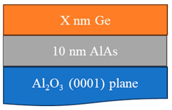
Figure 1.
Schematic of Ge thin film growths with different “X” thicknesses.
3. Results and Discussion
The Ge surface of each of the samples was analyzed in situ during growth using reflection high energy electron diffraction (RHEED). For example, the RHEED patterns for the four different Ge buffer thicknesses are shown in Figure 2. Diffraction spots were observed in the RHEED images during the initial nucleation stage of AlAs (Figure 2b) and Ge (Figure 2c,d), which indicates a three-dimensional (3D) surface of Ge as well as its (111) out-of-plane orientation [21,22,23]. The existence of twin domains is concluded from the presence of two distinct sets of diffraction peaks. These are labeled with green and blue circles on the simulated RHEED patterns (Figure 2e), which assumes twin domains rotated by 60° with respect to each other around the [111] axis of Ge. As the growth proceeded, the 3D RHEED pattern eventually evolved into a mixed spotty/streaky pattern (Figure 2f), which indicated a developing smoother surface with growth. The two middle stronger points are shown as half green and half blue because they were a result of both twins. With increasing the thickness of the Ge film, we observed several additional reflections on the RHEED pattern (Figure 2g). Our simulations (Figure 2h) indicate that these corresponded to additional twinning with growth that appeared around the [], [], [], and [] axes located in different domains in the Ge film.
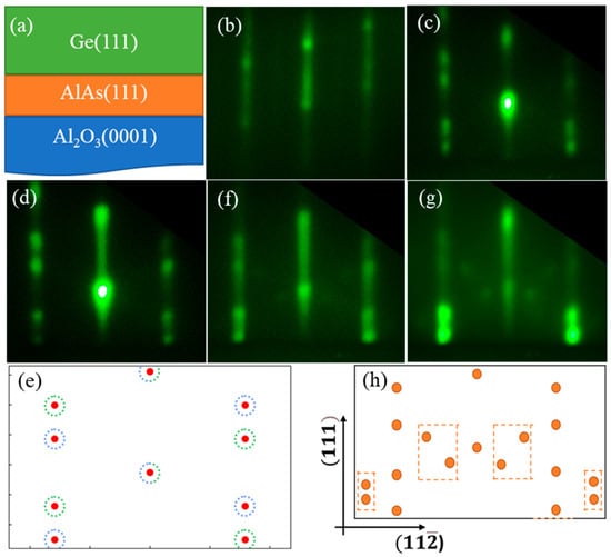
Figure 2.
(a) Schematic sample structure; (b) RHEED pattern of AlAs; (c,d,f,g) RHEED patterns after 1 min, 5 min, 30 min, and 120 min of Ge deposition; and (e,h) simulated RHEED patterns considering rotations of twin domains around [], [], [], and [].
X-ray diffraction (XRD) measurements were performed to study the crystal structure of the Ge layers after growth. For all of the samples, Figure 3a shows the symmetrical ω/2θ scans in which ω = θ. Hence, the direction of the scan of the diffraction vector was perpendicular to the sample surface and only the surface-symmetric planes were observed. As a result, the Ge (111) peak is seen along with the Al2O3(0006) peak, indicating that the out-of-plane orientation of Ge was (111). The Ge (111) peak was in proximity to the position of the bulk Ge (vertical dashed line), indicating a low level of strain (~ 0.2 ± 0.1%) in the Ge structure of all of the samples. Common to the x-ray diffraction from all of the samples, the shoulder at the right side of the Ge (111) peak corresponded to the thin AlAs layer. This was confirmed by the growth of a reference sample without the AlAs 10 nm wetting layer, for which the shoulder peak was not observed on the XRD spectrum [10].
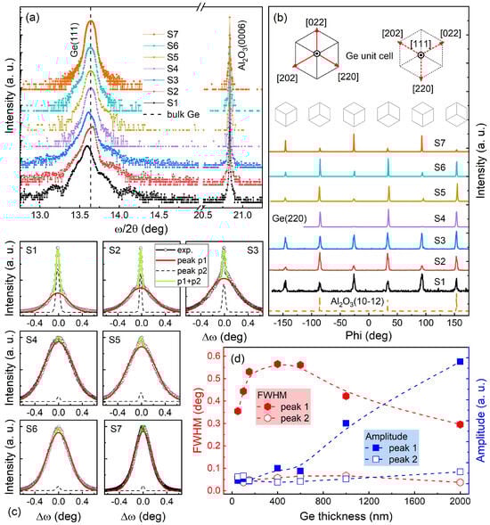
Figure 3.
X-ray diffraction analysis of the Ge crystal structure: (a) symmetrical ω/2θ scan and (b) phi scans for the Ge (220) and Al2O3 (102) reflections. Inset shows the projections of the Ge unit cell in the [111] direction for twin domains rotated by 180°. (c) Gaussian fitting of the ω spectrum of Ge (111) plane and (d) FWHM and amplitude as a function of thickness.
The azimuthal orientation of Ge (111) and its epitaxial relationship with the Al2O3 (0001) substrate were also studied using the XRD phi scan (φ-scan) measurements (Figure 3b). By performing a φ scan, an () plane was brought into the Bragg diffraction condition as the sample was rotated around the φ axis (surface normal). For the {220} family of planes of Ge epitaxial films, only a set of three planes, (220), (202), and (022), were expected to satisfy the Bragg diffraction condition when performing a φ scan of 360° [24]. Therefore, the emergence of the six Ge peaks in Figure 3b was attributed to twin grains observed for samples S1 to S3 that were rotated 60° with respect to each other (inset in Figure 2b), consistent with the RHEED observations during growth (Figure 2). Additionally, the epitaxial relationship between the epilayer and substrate was established using the φ scan data for the Al2O3 () reflection. The alignment of the Ge (220) and Al2O3 peaks was consistent with two epitaxial relationships, Ge (111)[110] parallel to Al2O3 (0001)[] and Ge (111)[110] parallel to Al2O3 (0001)[], both corresponding to a huge lattice mismatch of 42%. Further growth for S4 to S7 indicates a transition to favor a single twin.
The structural quality of the Ge epilayers was also investigated by comparing the linewidth of the XRD ω scan of the Ge (111) plane. The potential factors determining the linewidth were the lateral correlation length, density of dislocations, and tilt angles [25,26,27,28]. Figure 3c shows a complex diffraction pattern that could be deconvolved into a narrow and broad peak. The linewidth of the broad peak was 0.35 deg for the 50 nm sample and was shown to increase with the Ge layer thickness for S1 to S3, but decrease for S4 to S7 (Figure 3d), while the narrow component remained the same. Consistent with representing two different effects, the plot of the amplitude of each component versus thickness shows an increase for the broad peak with increasing Ge thickness while the relative amplitude of the narrow peak remained nearly the same. As a hypothesis, we took the narrow peak to represent the early stage of growth for each sample, while the broader peak represented growth above about 50 nm and depended on thickness.
To investigate further, characterization using Raman spectroscopy (RS) was performed to examine the strain in each sample. In contrast with the deep penetration of x-rays through the Ge samples, the penetration depth of the He-Ne laser beam used in the Raman study was only about 40 nm due to the high absorption coefficient of the Ge lattice [21]. Therefore, the Raman results were representative of the topmost layers of the Ge samples, and, in particular, the near-surface strain state of the Ge films, allowing for the study of strain as a function of growth. Figure 4a shows the Raman spectra of each film compared with the bulk Ge. A single peak was seen at around 300 cm−1 [29,30], which corresponded to the triply degenerated mode of symmetry F2g of the Ge cubic structure. This was the most intense first-order mode of the Ge lattice, and the lack of a commonly reported low-frequency adjacent band attributed to a disorder-activated origin confirmed the absence of an amorphous Ge phase [31] within the analyzed crystal volume. The frequency of the Ge (F2g) mode was used to estimate the in-plane strain () in each sample using the deformation potential of the F2g symmetry for the Ge lattice ( = = 415 cm−1) [32]. The strain behavior as a function of film thickness (Figure 4b) indicated relatively unstrained Ge islands for sample S1, followed up by strain build up for the Ge layer of samples S2 and S3, and strain relief starting with S4. Our data on twinning, omega linewidth, AFM, and Raman, as a function of thickness (Figure 4a) suggest that strain built for samples S1 to S3 at the boundaries between twinned grains. Note that the Ge grains of sample S1 were relatively freestanding. This was followed by a decrease in strain from S4 to S7, which was correlated to the transition to a single twin structure that then continued as a function of thickness resulting in an improvement in material quality as evidenced by the observed behavior (Figure 3c,d) of the linewidth of the broad component of the deconvolved peaks of the omega scan. At the same time, the three-dimensional structures or grains observed using atomic force microscopy (AFM) of each surface (Figure 5a) became more well defined in shape and direction as a function of Ge deposition and ripening.
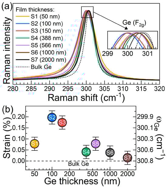
Figure 4.
(a) Raman spectra showing the Ge (F2g) mode of each sample compared with the relaxed mode of a bulk Ge structure. (b) Values of in-plane strain calculated from the frequency of the Ge (F2g) mode.
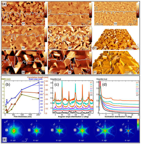
Figure 5.
(a) AFM images of germanium films with varying thicknesses (samples S1–S7), along with cross-sectional profiles of the surface relief and 3D reconstructions for samples S1 and S7. (b) Surface roughness (RMS), average grain size, and correlation length as a function of Ge film thickness for samples S1–S7. (c–e) Surface facet analysis, including in-plane orientations and tilt distributions, as well as associated bivariate histograms summarizing these distributions.
To investigate further, the nature of the orientational anisotropy and definition of the grain boundaries were illustrated by plotting the bivariate polar histograms of the local surface slope and direction obtained using AFM. Figure 5e indicates that a more well-defined geometry was developed with increased Ge film thickness. The increasing space between twin domains, correlation length, domain size, and surface smoothness; decreasing strain omega line width; and transition to single twin (Figure 3b) all indicate an improving quality of the Ge film with increasing film thickness. When the thickness of the germanium film reached 400 nm (S4), pronounced faceting was observed along with a transition to only one of the twins. The roughness and grain size consistently increased from samples S4 to S6. However, for S7, there was a noticeable reduction in roughness and observation of photoluminescence (PL). With further growth, strain relaxation occurred as the grains became well-defined and separated, the omega linewidth decreased, and we observed PL (Figure S1 in supporting information). However, the PL for samples S4 to S7 was weak and each shifted a bit from each other, possibly due to a different degree of strain for different layers, indicating the need for further study. The correlation length, depicted in Figure 5b, provided information on the correlated lateral spacing of the surface features. As expected, this length increased with the maturation of the three-dimensional structures [33]. It also showed a reduction in the lateral spacing of the surface features for sample S7.
A more statistical characterization of surface facets could be achieved through the analysis of the angular slope and local inclination distributions, as shown in Figure 5c,d. Measurements capturing the local in-plane slope orientation (φ) and vertical inclination (or tilt, θ) from the AFM image were consolidated into bivariate histograms, which depicted facet in-plane orientations and inclinations (see Figure 5e). As evident from Figure 5c,e, even the thinnest Ge layer displayed a subtle six-fold preferential in-plane orientation of grain boundaries. As the film thickness increased, the maxima of the angular slope distribution and the rays in the bivariate histograms became more defined. By the time the film reached a thickness of 2000 nm (S7), the crystallographic orientations of the surface grain edges became distinctly delineated.
Additionally, the bivariate histograms for samples S6 and S7 revealed nodes in the rays, which indicated a favoured tilt of the facets. This was further highlighted by the broad maxima in Figure 5d for samples S6 and S7. These histograms can be juxtaposed with the stereographic projection of Ge(111) presented in Figure 6. A facet tilt of 15.8 degrees aligned with the surface orientation (122), while a tilt of 8.5 degrees corresponded to the orientation (577). Given the symmetry of a regular triangle, added symmetry in the histograms emerged due to the simultaneous presence of step-up and step-down features in the same direction. This mirrored the existence of two opposing orientations of regular triangles, as depicted in Figure 6a (bottom right). It is worth noting that the facets characterized by orientation (577) correlated with road-like surface relief patterns, which might be linked to certain stacking faults [34].
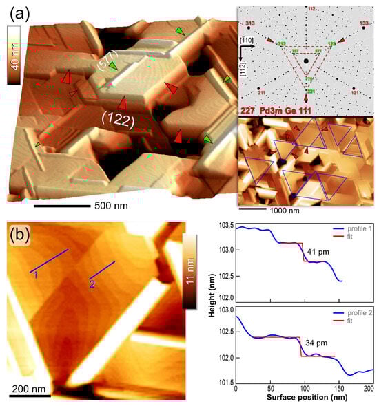
Figure 6.
(a) Crystallography of the surface grain facets in S7 and equivalent crystallographic planes (122) and (577) are marked. To right is the Wulff plot and AFM images of the (111) stereographic projection. (b) terraces as seen from faceted grains and heights of monatomic terraces.
The RS measurements indicate a relaxation of residual strains in samples S4 through S7. This strain relaxation manifested in the surface relief, signifying a shift from the 3D Volmer−Weber growth mechanism to a hybrid growth mode combining both 3D and two-dimensional step-flow growth. Distinct growth terraces were observable on the faceted grains, as depicted in Figure 6b. These monatomic terraces had heights ranging from 30 to 40 pm, aligning with the interplanar spacing of 32.7 pm in germanium along the <111> direction.
As a result, we observed a correlation between strain, quality, and twinning, and the interface between domains that suggest the interface between twin domains resulted in strain, broad omega line width, and the absence of PL. With further growth, stain relaxation occurred as the grains became well-defined and separated, the omega linewidth decreased, and we observed PL. For example, the 50 nm thick Ge film (S1) exhibited an RMS roughness of 5.5 nm. Table 1 summarizes the pattern for the seven different Ge film thicknesses.

Table 1.
Summary of the structural properties for all of the samples.
The microstructure of the Ge film was investigated in more detail through TEM analysis. Figure 7a shows a bright-field image of sample S4 taken under multi-beam conditions, allowing for most defects to be visible. Figure 7b is a HRTEM image taken along [112] of Ge and it confirms that this direction was parallel to [1120] of sapphire, in agreement with the XRD analysis. This image attests to the good mono-crystallinity of the Ge layer. Overall, the Ge epilayer was of good crystalline quality despite a high density of twin domains, as depicted by the blue and red broken lines in Figure 7a.
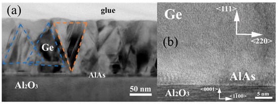
Figure 7.
(a) BF image of the Ge epilayer of a Ge/AlAs/Al2O3 sample obtained under multi-beam conditions showing twins marked with blue and red lines. (b) HRTEM image of the Ge/Al2O3 interface showing a good crystalline quality.
4. Conclusions
We report a study on the MBE growth of crystalline Ge on Sapphire (Al2O3 (0001)) substrates as a function of Ge thickness that utilized a 10 nm AlAs buffer layer. The Ge epilayer started with growth along the <111> direction with ubiquitous 60° (180°) rotating twin domains. In addition, as the growth of Ge progressed and reached a thickness of 400 nm, we observed significant changes in strain, twining, omega line width, surface roughness, and correlation length. This change in behavior was correlated with the formation of well-defined Ge grains, which was evidenced by the TEM image and the presence of PL signals, although their intensity was weak. The resulting sapphire/AlAs/Ge substrates developed here are now of sufficient quality to support the growth of GeSn thin films for several applications.
Supplementary Materials
The following supporting information can be downloaded at: https://www.mdpi.com/article/10.3390/cryst13111557/s1, Figure S1: The 10 K PL spectrum of sample S4 in comparison with a Ge refence sample.
Author Contributions
Conceptualization, E.W., S.-Q.Y. and G.J.S.; methodology, E.W., H.S. and F.M.d.O.; software, E.W. and H.S.; validation, E.W., H.S. and G.J.S.; formal analysis, E.W., P.L., F.M.d.O., H.S., Y.I.M. and M.B.; investigation, E.W., C.G., M.Z.-A., S.D., N.E., C.L. and S.S.; resources, E.W., M.Z.-A., C.G. and S.S.; data curation, E.W., P.L., H.S., F.M.d.O., M.B. and C.G.; writing—original draft preparation, E.W., H.S., F.M.d.O. and C.G.; writing—review and editing, E.W., H.S., F.M.d.O., P.L., C.G., S.S., S.D., N.E., C.L., M.Z.-A., M.B., Y.I.M., S.-Q.Y. and G.J.S.; visualization, E.W. and H.S.; supervision, S.-Q.Y. and G.J.S.; project administration, S.-Q.Y. and G.J.S.; funding acquisition, S.-Q.Y. and G.J.S. All authors have read and agreed to the published version of the manuscript.
Funding
This project was funded by the Navy, titled “SiGeSnPb Semiconductor Fab for Room Temp Electro-Optic Infrared (IR) Sensors.” Sponsor Award ID: N00014-23-1-2008.
Data Availability Statement
Not applicable.
Acknowledgments
The authors would like to acknowledge Sudip Acharya and Abdulla Ali Said from Material Science and Engineering at the University of Arkansas for their assistance with PL measurements.
Conflicts of Interest
The authors declare no conflict of interest.
References
- Marpaung, D.; Yao, J.; Capmany, J. Integrated microwave photonics. Nat. Photonics 2019, 13, 80–90. [Google Scholar] [CrossRef]
- Olorunsola, O.; Said, A.; Ojo, S.; Abernathy, G.; Saha, S.; Wangila, E.; Grant, J.; Stanchu, H.; Acharya, S.; Du, W.; et al. Enhanced carrier collection efficiency of GeSn single quantum well towards all-group-IV photonics applications. J. Phys. D Appl. Phys 2022, 55, 305101. [Google Scholar] [CrossRef]
- Olorunsola, O.; Said, A.; Ojo, S.; Stanchu, H.; Abernathy, G.; Amoah, S.; Saha, S.; Wangila, E.; Grant, J.; Acharya, S.; et al. SiGeSn quantum well for photonics integrated circuits on Si photonics platform: A review. J. Phys. D Appl. Phys. 2022, 55, 443001. [Google Scholar] [CrossRef]
- Olorunsola, O.; Stanchu, H.; Ojo, S.; Wangila, E.; Said, A.; Zamani-Alavijeh, M.; Salamo, G.; Yu, S. Optical and structural properties of GeSn/SiGeSn multiple quantum wells for infrared optoelectronics. J. Cryst. Growth 2022, 588, 126675. [Google Scholar] [CrossRef]
- Mingchu, T.; Siming, C.; Jiang, W.; Qi, J.; Vitaliy, G.D.; Mourad, B.; Yuriy, I.M.; Gregory, J.S.; Alwyn, S.; Huiyun, L. 1.3-μm InAs/GaAs quantum-dot lasers monolithically grown on Si substrates. Opt. Express 2011, 19, 11381–11386. [Google Scholar] [CrossRef]
- Du, W.; Ghetmiri, S.A.; Margetis, J.; Al-Kabi, S.; Zhou, Y.; Liu, J.; Sun, G.; Soref, R.A.; Tolle, J.; Li, B.; et al. Investigation of optical transitions in a SiGeSn/GeSn/SiGeSn single quantum well structure. J. Appl. Phys. 2017, 122, 123102. [Google Scholar] [CrossRef]
- Takuro, F.; Tomonari, S.; Koji, T.; Koichi, H.; Takaaki, K.; Shinji, M. Epitaxial growth of InP to bury directly bonded thin active layer on SiO2/Si substrate for fabricating distributed feedback lasers on silicon. IET Optoelectron. 2015, 9, 151–157. [Google Scholar] [CrossRef]
- Kim, Y.M.; Dahlstrom, M.; Lee, S.; Rodwell, A.J.W.; Gossard, A.C. High-performance InP/In/sub 0.53/Ga/sub 0.47/As/InP double HBTs on GaAs substrates. IEEE 2002, 23, 297–299. [Google Scholar] [CrossRef]
- Billah, M.R.; Blaicher, M.; Hoose, T.; Dietrich, P.I.; Marin-Palomo, P.; Lindenmann, N.; Nesic, A.; Hofmann, A.; Troppenz, U.; Moehrle, M.; et al. Hybrid integration of silicon photonics circuits and InP lasers by photonic wire bonding. Optica 2018, 5, 876–883. [Google Scholar] [CrossRef]
- Wangila, E.; Saha, S.K.; Kumar, R.; Kuchuk, A.; Gunder, C.; Amoah, S.; Khiangte, K.R.; Chen, Z.; Yu, S.Q.; Salamo, G.J. Single crystalline Ge thin film growth on c-plane sapphire substrates by molecular beam epitaxy (MBE). CrystEngComm 2022, 24, 4372–4380. [Google Scholar] [CrossRef]
- Al-Kab, S.; Ghetmiri, S.A.; Margetis, J.; Pham, T.; Zhou, Y.; Dou, W.; Collier, B.; Quinde, R.; Du, W.; Mosleh, A.; et al. An optically pumped 2.5 μm GeSn laser on Si operating at 110 K. Appl. Phys. Lett. 2016, 109, 171105. [Google Scholar] [CrossRef]
- Margetis, J.; Al-Kabi, S.; Du, W.; Dou, W.; Zhou, Y.; Pham, T.; Grant, P.; Ghetmiri, S.; Mosleh, A.; Li, B.; et al. Si-Based GeSn Lasers with Wavelength Coverage of 2–3 μm and Operating Temperatures up to 180 K. ACS 2017, 5, 827–833. [Google Scholar] [CrossRef]
- Schwank, J.R.; Ferlet-Cavrois, V.; Shaneyfelt, M.R.; Paillet, P.; Dodd, P.E. Radiation Effects in SOI Technologie. IEEE 2003, 50, 522–538. [Google Scholar]
- Kashfia, H.; Paul, B. A radiation hard configuration memory with auto-scrubbing. In Proceedings of the IECON 2011-37th Annual Conference of the IEEE Industrial Electronics Society, Melbourne, Australia, 7–10 November 2011; IEEE: New York, NY, USA. [Google Scholar] [CrossRef]
- Ashim, D.; Ali, R.; Frédéric, P.; Ananth, Z.S.; Stéphane, C.; Nicolas, L.T.; Roel, B. Efficiency of evanescent excitation and collection of spontaneous Raman scattering near high index contrast channel waveguides. Opt. Express 2015, 23, 27391–27404. [Google Scholar]
- O’Mahony, D.; Hossain, M.N.; John, J.; Emanuele, P.; O’Riordan, A.; Brendan, R.; Brian, C. High index contrast optical platform using gallium phosphide on sapphire: An alternative to SOI? SPIE 2012, 8431, 84311H-8. [Google Scholar]
- Tom, B.; Alexander, S.; Rob, I.; Andrew, S.; Boyan Penkov William, A.; Michael, H. Silicon-on-sapphire integrated waveguides for the mid-infrared. Opt. Express 2010, 18, 12127–12135. [Google Scholar] [CrossRef]
- Humphreys, T.P.; Miner, C.J.; Posthill, J.B.; Das, K.; Summerville, M.K.; Nemanich, R.J.; Sukow, C.A.; Parikh, N.R. Heteroepitaxial growth and characterization of GaAs on silicon-on-sapphire and sapphire substrates. Appl. Phys. Lett. 1989, 54, 1687–1689. [Google Scholar] [CrossRef]
- Xia, C.; Milosevic, S.M.M.; Scott, R.; Thalía, D.B.; Ke, L.; David, J.T.; Frederic, G.; Graham, T.R. The emergence of Silicon Photonics as a Flexible Technology Platform. IEEE 2018, 106, 2101–2116. [Google Scholar]
- Saha, S.K.; Kumar, R.; Kuchuk, A.; Alavijeh, M.Z.; Maidaniuk, Y.; Mazur, Y.I.; Yu, S.; Salamo, G.J. Crystalline GaAs Thin Film Growth on a c-Plane Sapphire Substrate. Cryst. Growth Des. 2019, 19, 5088–5096. [Google Scholar] [CrossRef]
- Littlejohn, A.J.; Xiang, Y.; Rauch, E.; Lu, T.-M.; Wang, G.-C. van der Waals epitaxy of Ge films on mica. J. Appl. Phys. 2017, 122, 185305. [Google Scholar] [CrossRef]
- Khiangte, K.R.; Rathore, J.S.; Schmidt, J.; Osten, H.J.; Laha, A.; Mahapatra, S. Wafer-scale all-epitaxial GeSn-on-insulator on Si(1 1 1) by molecular beam epitaxy. J. Appl. Phys. 2018, 51, 32LT01. [Google Scholar] [CrossRef]
- Ichimiya, A.; Cohen, P.I. Reflection HighEnergy ElectronDiffraction; John Wiley & Sons, Ltd.: Hoboken, NJ, USA, 2005; Volume 22, pp. 2769–2770. [Google Scholar] [CrossRef]
- Kim, H.J.; Duzik, A.; Hyung, B.; Choi, S.H.; Zhao, Y. High-Electron-Mobility SiGe on Sapphire Substrate for Fast Chipsets. ProQuest Cent. 2008, 2015, 785415. [Google Scholar] [CrossRef][Green Version]
- Moram, M.A.; Vickers, M.E. X-ray diffraction of III-nitrides. Rep. Prog. Phys. 2009, 72, 036502. [Google Scholar] [CrossRef]
- Kim, H.J.; Duzik, A.; Choi, S.H. Lattice-alignment mechanism of SiGe on Sapphire. Acta Mater. 2018, 145, 1–7. [Google Scholar] [CrossRef]
- Poulat, S.; Ernst, F. Epitaxy of Ge on sapphire. Mater. Sci. Eng. A 2001, 323, 9–16. [Google Scholar] [CrossRef]
- Godbey, D.J.; Twigg, M.E. The nucleation and growth of germanium on (1102) sapphire deposited by molecular beam epitaxy. J. Appl. Phys. 1991, 69, 4216–4221. [Google Scholar] [CrossRef]
- Joshua, G.; Abernathy, G.; Olorunsola, O.; Ojo, S.; Amoah, S.; Wanglia, E.; Saha, S.; Sabbar, A.; Du, W.; Alher, M.; et al. Growth of Pseudomorphic GeSn at Low Pressure with Sn Composition of 16.7%. Materials 2021, 14, 7637. [Google Scholar] [CrossRef]
- Kartopua, G.; Bayliss, S.C. Simultaneous micro-Raman and photoluminescence study of spark-processed germanium: Report on the origin of the orange photoluminescence emission band. Appl. Phys. Lett. 2004, 95, 3466–3472. [Google Scholar] [CrossRef]
- Krivyakin, G.K.; Volodin, V.A.; Kamaev, G.N.; Popov, A.A. Effect of Interfaces and Thickness on the Crystallization Kinetics of Amorphous Germanium Films. Semiconductors 2020, 54, 754–758. [Google Scholar] [CrossRef]
- Ghosh, A.; Clavel, M.B.; Nguyen, P.D.; Meeker, M.A.; Khodaparast, G.A.; Bodnar, R.J.; Hudait, M.K. Growth, structural, and electrical properties of germanium-on-silicon heterostructure by molecular beam epitaxy. AIP Adv. 2017, 7, 095214. [Google Scholar] [CrossRef]
- Maity, G.; Yadav, R.P.; Singhal, R.; Sulania, I.; Mitta, A.K.; Chaudhary, D.K. Thickness effect on scaling law and surface properties of nano-dimensional SnTe thin films. J. Appl. Phys. 2021, 130, 175306. [Google Scholar] [CrossRef]
- Tramposch, R.F. Epitaxial Films of Germanium Deposited on Sapphire via Chemical Vapor Transport. J. Electrochem. Soc. 1969, 116, 654. [Google Scholar] [CrossRef]
Disclaimer/Publisher’s Note: The statements, opinions and data contained in all publications are solely those of the individual author(s) and contributor(s) and not of MDPI and/or the editor(s). MDPI and/or the editor(s) disclaim responsibility for any injury to people or property resulting from any ideas, methods, instructions or products referred to in the content. |
© 2023 by the authors. Licensee MDPI, Basel, Switzerland. This article is an open access article distributed under the terms and conditions of the Creative Commons Attribution (CC BY) license (https://creativecommons.org/licenses/by/4.0/).