Abstract
Photovoltaic cells, based on quantum dots implementation in the intrinsic region, are one of the most widely studied concepts nowadays to obtain a high solar conversion efficiency. The challenge in this third generation of solar cells is to find a good combination of materials that allows obtaining higher efficiency with low cost. In this study, we consider a juxtaposition of two kinds of quantum dots (dot/barrier) inside the I region of the PIN junction: the first combination of semiconductors includes the two configurations, PbTe/CdTe and PbSe/ZnTe, and the second combination is InN/GaN. Thus the intermediate band can be tailored by controlling the size of the dots and the inter-dot distances. The principal interest of this investigation is to determine the optimized parameters (the dot size and the inter-dot distance), leading to obtain a better solar cell efficiency. Intermediate bands, their positions, and their widths, are determined using 3D confined particles (electron and hole). Their energy levels are determined by solving the Schrödinger equation and solving the well-known dispersion relation in the Kronig–Penney model.
1. Introduction
Photovoltaic conversion is the direct transformation of solar electromagnetic energy into electrical energy. It can constitute a substantial part of electricity production, in particular as a replacement for production that emits many greenhouse gases. It can also alleviate the country’s energy dependence on fossil fuels. Faced with the scarcity of traditional polluting energies and the challenge of developing a clean energy respecting the environment, the race against time to achieve solar cells with efficiencies much greater than that of the classic Shockley–Queisser limit (30%) of a single junction, characterized by a single band gap, remains a challenge for scientists and industrials. The expansion of photovoltaic technology known as “solar cell band engineering” [1,2] is leading to new generations of these optoelectronic devices. Although these new generations are in the embryonic state, their future is surely guaranteed given the growing progress in chemistry, growth technologies and the mastery of nanomaterials.
The efficiency of the photovoltaic conversion process in the case of the first generation essentially based on mono or poly-crystalline silicon does not exceed 26.7%, while the second generation based on III-V semiconductors can reach up to 29% [3,4]. The thin films of the II–VI compounds, mainly CdTe, also showed an efficiency approximately equal to 21% [3,5]. This generation also includes solar cells based on CuInSe and CuGaInSe, known as (CIGS) and CuInS, based on elements of groups (I, III and IV) of the periodic table. These materials were chosen due to their direct gap and their high optical absorption coefficient. They allow to obtain yields around 23.3% [3]. Among the second generation, let us note the existence of several other types of cells in the so-called hybrid solar cells made by mixing organic and inorganic materials cells with a large-gap dye type (TiO, ZnO, NbO). They reach yields of 11.9% and are interesting because of their low production costs, but unfortunately they still have problems in terms of degradation under the effect of heat and UV, organic solar cells with high efficiency 12.6% [3] and hybrid perovskite and perovskite cells, which are materials of formula ABX. They all have the advantage of being able to be developed by solution processes and of being deposited on flexible substrates. To date, the highest efficiencies with this system are 21.6% [3].
The third generation include multijunction layouts, which demonstrated current record values of 38.8% in III–V systems and 28% in perovskite-on-silicon systems [3] and solar cells with intermediate levels [6,7]. This concept introduced by Luque and Martí [8] is based on the creation of one or more energy levels in the band gap such that they absorb low energy photons in parallel with the normal photodiode process.
These additional states may exist as discrete energy levels or as a sub-band, separated from the conduction (CB) band and valence band (VB). Such an operation leads to a theoretical limit yield, similar to that obtained in the three-level tandem cell (63% under maximum concentration).
This simple but ingenious process known as quantum dot intermediate band solar cell (QD-IBSC) can be described as follows: even low photon energies can contribute to traversing the gap step by step (VB → IB → CB), while high energy photons are absorbed between (VB) and (CB). To collect the carriers generated after impact of the photons, it is necessary for the intermediate band material to be between two semiconductors of the p and n type, respectively. A simple way to create this intermediate band is to implement quantum dots formed by the juxtaposition of two materials (A/B) in the intrinsic region of the P-I-N junction. The first material (A) has the lowest band gap value and constitutes the quantum well (with a diameter of 5 to 15 nm). The second semiconductor (B) constitutes the barrier material.
Until now, the vast majority of QD-IBSC prototypes have been realized using type-I QDs. In particular, significant experimental studies have investigated the two-step absorption mechanism in several materials: InAs/GaAs QD system [9], GaAs/AlGaAs [10] and InAs/AlGaAs [11]. Lately, the same process was reported in a single InAs/GaAs QD [12,13,14,15,16,17]. The maximum efficiency of colloidal QDSC recently achieved a world record of % using perovskite QDs system [18]. Recently, organic photovoltaic cells have marked an increase in photovoltaic conversion by using different types of donor and acceptor combinations [19,20,21]. We recall that in an ideal IBSC, the photogenerated current (J) should be improved with slight diminution in the open-circuit voltage (V) [8].
Even so, almost all manufactured devices show low V [22]. The reason for this voltage diminution remarked in QD-IBSC devices is assigned to the nonradiative recombination related to the structural defect in the lattice of QDs [23], the charge transfer processes at the QD-Barrier mismatch and finally the radiative recombination in the barrier [24,25], and the capture and radiative recombination through QDs of carriers photogenerated in the barrier [26,27]. Practically, to realize an intermediate band solar cell (IBSC), some specific material systems were proposed, semiconductor alloys [15,28,29,30], semiconductor superlattice [31], quantum dots [9,32] and dopant impurities [33]. Despite these advances, the challenge is still open, especially toward new combinations of nanomaterials in the hope of increasing the efficiency of photovoltaic conversion. The mastery of solar cell technology passes through the control of different properties, such as the nature and size of materials.
The aim of this study is to try to find the good combination of semiconductor materials, which makes it possible to achieve an efficiency close to the theoretical limit of the IBSCs. In order to create the IBSC, we consider a juxtaposition of two kinds of QD: the first combination of semiconductors, so called the lead salt of QDs, is taken as the family (IV-VI) embedded in (II-VI) semiconductors (PbTe/CdTe, PbSe/ZnTe), and the second combination is the III-N semiconductor materials (InN/GaN). The advantages of the IV-VI/II-VI QD materials for the implementation of the IBSC are (i) there is no wetting layer, (ii) in the II-VI group, there are direct-gap materials with a much larger gap, and (iii) nonradiative recombining defects are minimized because the QD and host materials are close to lattice matching [34]. More details concerning these material systems can be found in the literature [6,34,35,36]. We report on the electronic properties and photonic characteristics of QD-IBSCs based on these material systems and analyze their performance dependence on the QD size. Calculations are performed under the detailed balance theory [8,37,38]. This approach considers some important assumptions, which are currently challenges to the scientific community working on the experimental processing of quantum dot solar cells. In particular, a negligible impact of defects at materials and interfaces on device is considered, implying a very long minority carrier lifetime and diffusion length. As a result, losses are only due to radiative recombination, where band-to-band transitions take place. In addition, there are no losses from radiation reflection, and ideal series and shunt resistances are assumed. In this sense, these conditions allow to study the maximum efficiencies expected for these technologies. The organization of this manuscript is the following: In Section 2, the theoretical framework for intermediate band solar cells is developed. In Section 3, the numerical results regarding a comparative analysis of different materials are given. Finally, the conclusions are provided in Section 4.
2. Theoretical Framework
2.1. Photonic Properties
Figure 1 shows the pictorial model of our structure. The cubic quantum dots are placed in the I-region of the P-I-N junction immersed in a matrix. This system is described by two parameters: the sizes of the dot L and barrier H, as it is shown Figure 1. In the present work, we consider the following material systems: PbTe/CdTe, PbSe/ZnTe and InN/GaN.
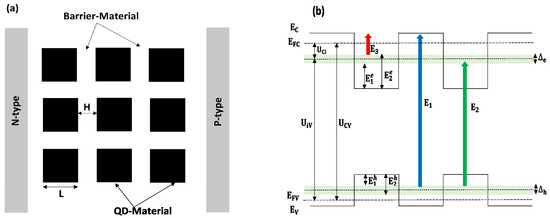
Figure 1.
(a) Schematic diagram of the QD-IBSC structure. The black cubes represent QD material, which are embedded into the barrier material. (b) Energy band diagram of the QD-IBSC where and denote the energies of CB and VB of the host material and represents its band gap. and are the energies of bottom and top sub-gaps, respectively, and () is the chemical potential between VB and IB (IB and CB). and are the IB widths of the electron and hole, respectively.
Now, let us determine the photonic properties. Thus, the photon-generated current for an ideal solar cell depends on the number of absorbed photons and emitted photons from the QD-IBSC. The current density of QD-IBSC can be expressed as [39,40,41]:
where is the geometric factor and is the solar concentration at a solar cell. The full concentration would be achieved when . We focus our investigation on the QD-IBSCs efficiencies with fully concentrated light . is the temperature of the sun (6000 K), is the temperature of the solar cell (300 K). is the flux of photons absorbed by or emitted from the semiconductor:
where U is the chemical potential, k is the Boltzmann constant, c is the light speed in vacuum, and and are the superior limit energy level and the lower limit energy level, respectively. From the IB, there is no current extracted. Therefore, the current entering the IB must be equal to the current leaving the IB. Consequently, the second term in Equation (1) becomes [39,42,43]:
For a P-I-N solar cell, the output voltage of a IBSC can be expressed as:
From Equations (1)–(4), it is observed that the effect of the bandwidth and position is evaluated through and , where corresponds to interband transitions, while stands for transitions from the band of electrons to the conduction band of the host material.
The fill factor is a function of and , and it is defined as the ratio of maximum power that can be extracted from a solar cell to the ideal power. It is given in terms of percentage, such as
where and are the maxima of the current density and voltage of the QD-IBSC, respectively. Thus, the QD-IBSC photovoltaic conversion efficiency is given by
where is the power density falling on QD-IBSC.
2.2. Electronic Properties
After determining the photonic properties of the QD-IBSC device, it is now time to study the system from an electronic point of view. In QDs, the 3D confined particles (electron and hole) energy levels are determined by solving the Schrödinger equation:
Let us recall that in our last study published recently [44], we developed an analytical calculation of efficiency in three types of QD shapes (cubic, spherical and cylindrical); we demonstrated that the efficiency is not very sensitive to the geometrical shape. Therefore, and for simplicity, we only analyze the case of cubic QDs. In this case, the 3D structure is considered a three-dimensional periodic super-crystal structure. In these conditions, and due to the indiscernibility of the three directions (x, y, z), and because , the 3D wave function can be written as a product of three 1D electronic wave functions:
while the total energy can be written as the sum of three equivalent electronic eigenenergies . Therefore, we can limit our problem to the x direction. Within the framework of the effective mass approximation, the Hamiltonian of a single electron (hole) in a QD can be written in the x direction as
The confinement potential is given by
The effective masses in the QD and in the barrier is given by
In this study, we used the spherical average between the transversal () and longitudinal () masses for calculating the effective masses of the rock-salt materials [34,45], where .
In order to determine both electron and hole energies and to obtain the optimized IB position and width to achieve the maximum efficiency, we solve the well-known dispersion relation in one direction for electrons and holes by adopting the Kronig–Penney model [46]. So, for electron (hole) bound states,
and for unbound states, , becomes
where and are, respectively, and , such that and are, respectively, the effective masses in the well and the barrier.
With the aim of solar cell simulation, a software was developed using FORTRAN and Maple, which contains all equations, constants and parameters. From Equation (1), the J-V characteristics as function of simulation parameters are obtained and thus the optoelectronic properties are evaluated.
3. Results and Discussion
We start our discussion by investigating the confinement behavior of the different configurations on the fundamental levels of electron and heavy hole at the optimal inter-dot spacing H for each material ( nm, nm and nm for PbTe/CdTe, PbSe/ZnTe and InN/GaN QD materials respectively). Data were obtained from the literature and detail are presented in the table caption (Table 1) [45,47,48,49].

Table 1.
Physical parameters of the different material systems using in the present calculations.
As we can show in Figure 2, the increasing of the dot size L reduces both fundamental levels of electron and heavy hole because the quantum confinement is less with L increasing. Additionally, it is remarked that the first IB of both electron and heavy hole appears for PbSe/ZnTe and InN/GaN configurations for nm and the fundamental electron states (fundamental heavy hole states) are eV and eV ( eV and eV) for PbSe/ZnTe and InN/GaN, respectively. However, for PbTe/CdTe QD material, the IB appears for nm and the first electron state (heavy hole state) is eV ( eV). For calculations, the lowest spacing are required for a higher overlapping of wave functions corresponding to states and thus, the obtention of a bandwidth higher. The reduction of spacing between QDs will result in a higher absorption of photons due to a higher bandwidth, thereby increasing the short-circuit current density, and since carriers are no longer localized within QDs due to the formation of band, losses due to recombination are reduced, resulting in an efficiency promotion. In this sense, the study of the impact of different QDs sizes with the lowest interspacing between QDs would result in a global maximum. As we show in Figure 2, both electron and heavy hole are confined firstly in the PbSe/ZnTe followed by the case of InN/GaN, and lastly, in the PbTe/CdTe system material.
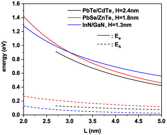
Figure 2.
Fundamental electron (solid lines) and heavy hole states (dashed lines) versus dot size L for different materials at the optimum inter-dot spacing nm, nm and 3 nm for PbTe/CdTe, PbSe/ZnTe and InN/GaN QD materials.
In Figure 3, we present the variation of the IB electron width as a function of both parameters L ans H for all considered system materials. As can be seen, tends to decrease as the dot size L and the inter-dot distance H increase. This decrease can be explained by the fact that the overlap quantized levels between different QDs become small, which can cause a decline in the transitional probabilities of photo-generated carriers from VB to CB via IBs. Additionally, the quantum effect on the low quantized levels is stronger than that of the higher ones. On the other hand, and by moving the QDs away, in other words, by increasing the inter-dot distance H, the width of the electron and IBs reduces until reaching a value close to zero. This behavior can be explained by the weak coupling of the wave functions of the more distant QDs. However, a larger IB width is beneficial in order to absorb more sunlight and therefore increase the current.
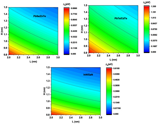
Figure 3.
A 2D contour plot of IB electron width as function, the dot size L and inter-dot distance H for different system materials.
We present in Figure 4 the variation of sub-band gap energies (solid lines) and (dashed lines) as the function of dot size L at the optimum inter-dot spacing H for each material ( nm, nm and nm for PbTe/CdTe, PbSe/ZnTe and InN/GaN QD materials, respectively). As it is seen, decreases with L increasing. The effect of low quantum confinement in broader QDs can explain this behavior. In fact, the fundamental state of electron becomes closer to the bottom of the potential well, as L increases, thereby affecting the value. For the transition, the reverse behavior is noted. The sub-band gap increases by increasing the dot size L for InN/GaN configuration, but for both PbSe/ZnTe and PbTe/CdTe materials, the sub-band gap grows up to nm and 4 nm, then decreases. This behavior is explained by the fact that in this study, our calculations are limited to the case where no second IB is observed. As a consequence, we have only taken into account the impact of one IB. If the second band appears, it is considered a conducting band. For third-generation solar cell devices, this optical transition is very important, as it allows low-energy photons to be absorbed, which is not possible in conventional solar cells. It is very important to note that we have limited our calculations in the present work to the case where no second IB is observed. As a result, we have only taken into account the impact of one IB. It would be considered to be a conducting band if the second band appeared. Therefore, we can observe a maximum of in the case of the two configurations: PbSe/ZnTe and PbTe/CdTe.
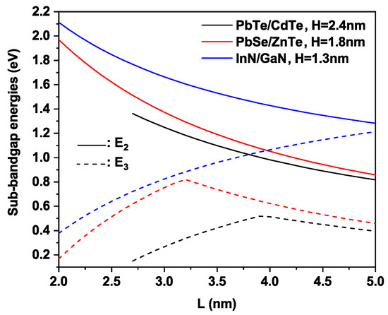
Figure 4.
Variation of the sub-band gap energies (solid lines) and (dashed lines) versus dot size L at the optimum inter-dot spacing nm, nm and nm for PbTe/CdTe, PbSe/ZnTe and InN/GaN QD materials.
The variation of (dashed lines) and (solid lines) versus the dot size L is illustrated in Figure 5 at the optimum inter-dot spacing H for each material ( nm, nm and nm for PbTe/CdTe, PbSe/ZnTe and InN/GaN QD materials, respectively). The enlargement in with dot size L can be attributed to the increase in generation rate. Larger dots lead to higher generation rates and broaden the range of photon energy, which can further result in a creation of electron–hole pairs that in turn boosts the . On the other hand, as the is dependent on the chemical potential between VB and CB, in other words, the host bandgap, the variation in L does not affect it, thus implies a weak dependence on L. As we have already mentioned in this study, our calculations are limited to the case where no second IB is observed. As a consequence, we have only taken into account the impact of one IB. If the second band appears, it is considered a conducting band. For that reason, we remark a decrease in in the case of PbSe/ZnTe and PbTe/CdTe systems at nm and nm, respectively. For the InN/GaN configuration and as we have already seen, the optical transition decreases by increasing the dot size L; on the other hand, the transition increases and they both converge around the value nm (see Figure 4). Therefore, decreases after nm in the case of the InN/GaN configuration.
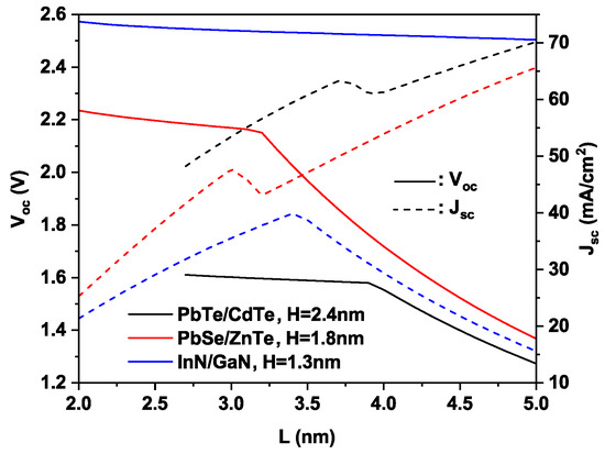
Figure 5.
Variation of (dashed lines) and (solid lines) versus dot size L at the optimum inter-dot spacing nm, nm and nm for PbTe/CdTe, PbSe/ZnTe and InN/GaN QD materials.
The photovoltaic efficiency is shown in Figure 6 as a function of the dot size L and for different configurations. As we can see, for all considered configurations, the efficiency increases to a maximum value and then decreases, while L tends to increase. Shao et al. [41] observed the same behavior patterns. This behavior can be explained by the fact that by increasing the dot size L, the IB position is affected, so the sub-band gaps and are affected. As L increases, more photons are absorbed, so the photo-generated current density of increases.
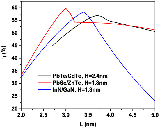
Figure 6.
Photovoltaic conversion efficiency of QD-IBSC structure versus dot size L for different material systems and for a fixed inter-dot size at the optimum inter-dot spacing nm, nm and nm for PbTe/CdTe, PbSe/ZnTe and InN/GaN QD materials.
In particular, for PbSe/ZnTe, the maximum efficiency is achieved for the optimum pair (L, H) ( nm and nm). For PbTe/CdTe configuration, the maximum efficiency of is reached for ( nm and nm). Lastly, for the InN/GaN QD material, the maximum efficiency of for ( nm and nm). Nevertheless, it is worth mentioning that the maximum efficiency is reached for the case of PbSe/ZnTe due to the fact that the combination of transitions ( eV and eV) is almost the same result found by Antolín et al. [34], where the maximum efficiency is for nm and the transitions are eV and eV). However, for PbTe/CdMgTe, the maximum efficiency for nm is reached (for eV and eV). Furthermore, in Table 2, we present the optimum parameters that characterize the photovoltaic device performance. The numerical results, which are estimated at room temperature (300 K), can be a guide for the experimental fabrication of this type of solar cells.
Table 2.
Optimum parameters and characteristics of the different material systems of the proposed QD-IBSC device.
In Figure 7, at the optimum pair (L and H) of different configurations, we illustrate the output power versus voltage between CB and VB that achieves maximum efficiency. With regard to the voltage, it increases until it reaches a maximum and then decreases quickly. Additionally, in the case of full concentrated light, higher values of both current density and open circuit voltage are theoretically achieved, leading to an enhancement in photovoltaic conversion efficiency. As showed in previous figures, the higher photovoltaic conversion efficiency are obtained in the case of PbSe/ZnTe configuration, followed by the case of InN/GaN system material, and then PbTe/CdTe QD-IBSC.
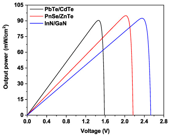
Figure 7.
Output power of the QD-IBSC at the full concentration at the optimum pair (L, H): ( nm, nm), ( nm, nm) and ( nmn nm) for PbTe/CdTe, PbSe/ZnTe and InN/GaN QD materials.
Now let us examine the J-V characteristics of the proposed QD-IBSC for different material systems at the optimum pair (L and H). It is worth mentioning that the short current density is directly linked to the QD containment system; meanwhile, the open-circuit voltage is restricted to , where q is the electron charge and is the material barrier gap. From Figure 8, it can be noticed that, compared to other cases, QD-IBSC based on PbTe/CdTe system material denotes higher and small voltage value. Nevertheless, and from a solar cell point of view, this behavior occurs because more photons are absorbed and more electrons are excited in the PbTe/CdTe system material case. In addition, an increased photogenerated current is achieved; the small value of the output voltage prevents the enhancement of power efficiency.
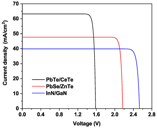
Figure 8.
Current density versus voltage between CB and VB of the QD-IBSC at the full concentration at the optimum pair (L, H): ( nm, nm), ( nm, nm) and ( nmn nm) for PbTe/CdTe, PbSe/ZnTe and InN/GaN QD materials.
Now let us analyze the effect of the inter-dot distance H on the performance of QD-IBSC proposed at the optimum dot size nm, 3 nm and nm for PbTe/CdTe, PbSe/ZnTe InN/GaN material systems, respectively. As indicated in Figure 9, by moving the QDs away, in other words, by increasing the inter-dot distance H, the energies and widen and the IB width decreases as shown in Figure 3. It is highly recommended in this regard to achieve an agreement between the high values of and and the smaller IB width values in order to absorb more sunlight and therefore increase the current.
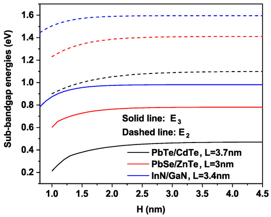
Figure 9.
Variation of the sub-band gap energies (solid lines) and (dashed lines) versus inter-dot size H at the optimum dot size nm, 3 nm and nm for PbTe/CdTe, PbSe/ZnTe and InN/GaN QD materials.
In Figure 10a, we present the variation of as a function of H at the optimum dot size L for different materials proposed. As observed, the decreases by increasing H. This behavior is due to the fact that the optical transitions and increase with decreasing and while increasing H. Therefore, few photons are absorbed, and then few number of electrons is excited, and the induced current density is lower.
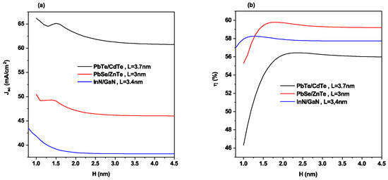
Figure 10.
(a) Variation of and (b) photovoltaic conversion efficiency of QD-IBSC structure versus H at the optimum dot size nm, 3 nm and nm for PbTe/CdTe, PbSe/ZnTe and InN/GaN QD materials.
The variation of photovoltaic efficiency as a function of H is shown in Figure 10b at the optimum dot size L for different materials proposed. As shown, for the range of nm ≤ H nm, increases and for H greater than nm, maintains its value. This behavior normally happens because with a small H, the IBs will acquire a high number of photons and it then excites a large number of electrons; high current density is induced. Therefore, efficiency is promoted. Then, by increasing H, the width of the intermediate band ( and ) decreases until it becomes an intermediate level; therefore, and take constant values for the different materials (Figure 9), so also takes constant values for the different materials.
4. Conclusions
The mastery of solar cell technology passes through the control of different properties and parameters, such as the nature and size of quantum materials. The extremely high photovoltaic conversion predicted for intermediate band solar cells by detailed balance calculations has not been reached. In this work, we present a theoretical study of the impact of the different QD materials on the QD-IBSC performance versus the inter-dot spacing, and dot size is presented using the Kronig–Penney model and based on parameters reported experimentally and theoretically. We considered a juxtaposition of two kinds of quantum dots: the first combination of semiconductors is taken as the family (IV-VI) embedded in (II-VI) semiconductors (PbTe/CdTe, PbSe/ZnTe), and the second combination is the III-N semiconductor materials (InN/GaN). This study shows that solar cell performance can be improved by changing the quantum dot system. In addition, it was shown that both the quantum dot size and the inter-dot distance play a key role in searching for the maximum efficiency of solar cells in the quantum dot intermediate band. It is found that the maximum efficiency is obtained for PbSe/ZnTe QD material, considering for nm and nm. For the case of the InN/GaN system material, the maximum efficiency is for nm and nm. Lastly, for PbTe/CdTe QD material, the maximum efficiency of is obtained for nm and nm. These findings add to a growing body of literature on the third generation of solar cells. Further studies, which take strain effect into account, will need to be performed.
Author Contributions
Conceptualization, L.M.P. and A.E.A.; methodology, F.D., V.T., M.C. and E.M.F.; software, A.E.A., K.F. and A.B.A.; formal analysis, F.D., D.L. and M.C.; investigation, A.E.A. and E.M.F.; data curation, L.M.P., A.E.A., K.F., J.A.R. and A.B.A.; writing—original draft preparation, M.C., A.E.A. and E.M.F.; writing—review and editing, L.M.P., D.L. and E.M.F.; visualization, A.E.A., K.F. and A.B.A.; project administration, E.M.F.; funding acquisition, L.M.P. and D.L. All authors have read and agreed to the published version of the manuscript.
Funding
LMP acknowledges financial support from ANID through Convocatoria Nacional Subvención a Instalación en la Academia Convocatoria Año 2021, Grant SA77210040. DL acknowledges partial financial support from Centers of excellence with BASAL/ANID financing, AFB180001, CEDENNA.
Data Availability Statement
The data presented in this study are available on reasonable request to the corresponding authors.
Conflicts of Interest
The authors declare no conflict of interest.
References
- Beattie, N.S.; See, P.; Zoppi, G.; Ushasree, P.M.; Duchamp, M.; Farrer, I.; Ritchie, D.A.; Tomic, S. Quantum engineering of InAs/GaAs quantum dot based intermediate band solar cells. ACS Photonics 2017, 4, 2745–2750. [Google Scholar] [CrossRef]
- Ramiro, I.; Martí, A. Intermediate band solar cells: Present and future. Prog. Photovoltaics Res. Appl. 2020, 29, 705–713. [Google Scholar] [CrossRef]
- Green, M.A.; Dunlop, E.D.; Hohl-Ebinger, J.; Yoshita, M.; Kopidakis, N.; Hao, X. Solar cell efficiency tables (Version 58). Prog. Photovoltaics Res. Appl. 2021, 29, 657–667. [Google Scholar] [CrossRef]
- Creti, A.; Tasco, V.; Montagna, G.; Tarantini, I.; Salhi, A.; Passaseo, A.; Lomascolo, M. Experimental Evidence of Complex Energy-Level Structuring in Quantum Dot Intermediate Band Solar Cells. ACS Appl. Nano Mater. 2020, 3, 8365–8371. [Google Scholar] [CrossRef]
- Polman, A.; Knight, M.; Garnett, E.C.; Ehrler, B.; Sinke, W.C. Photovoltaic materials: Present efficiencies and future challenges. Science 2016, 352, aad4424. [Google Scholar] [CrossRef] [Green Version]
- Wu, J.; Wang, Z.M. Quantum Dot Solar Cells; Springer: New York, NY, USA, 2014. [Google Scholar]
- Soga, T. Nanostructured Materials for Solar Energy Conversion; Elsevier: Amsterdam, The Netherlands, 2006. [Google Scholar]
- Luque, A.; Martí, A. Increasing the efficiency of ideal solar cells by photon induced transitions at intermediate levels. Phys. Rev. Lett. 1997, 78, 5014. [Google Scholar] [CrossRef]
- Martí, A.; Antolín, E.; Stanley, C.; Farmer, C.; López, N.; Díaz, P.; Cánovas, E.; Linares, P.; Luque, A. Production of photocurrent due to intermediate-to-conduction-band transitions: A demonstration of a key operating principle of the intermediate-band solar cell. Phys. Rev. Lett. 2006, 97, 247701. [Google Scholar] [CrossRef]
- Scaccabarozzi, A.; Adorno, S.; Bietti, S.; Acciarri, M.; Sanguinetti, S. eVidence of two-photon absorption in strain-free quantum dot GaAs/AlGaAs solar cells. Phys. Status Solidi RRL Rapid Res. Lett. 2013, 7, 173–176. [Google Scholar] [CrossRef]
- Tamaki, R.; Shoji, Y.; Okada, Y.; Miyano, K. Spectrally resolved interband and intraband transitions by two-step photon absorption in InGaAs/GaAs quantum dot solar cells. IEEE J. Photovoltaics 2014, 5, 229–233. [Google Scholar] [CrossRef]
- Nozawa, T.; Takagi, H.; Watanabe, K.; Arakawa, Y. Direct observation of two-step photon absorption in an InAs/GaAs single quantum dot for the operation of intermediate-band solar cells. Nano Lett. 2015, 15, 4483–4487. [Google Scholar] [CrossRef]
- Tomić, S.; Sogabe, T.; Okada, Y. In-plane coupling effect on absorption coefficients of InAs/GaAs quantum dots arrays for intermediate band solar cell. Prog. Photovoltaics Res. Appl. 2015, 23, 546–558. [Google Scholar] [CrossRef]
- Willis, S.; Dimmock, J.; Tutu, F.; Liu, H.; Peinado, M.; Assender, H.; Watt, A.; Sellers, I. Defect mediated extraction in InAs/GaAs quantum dot solar cells. Sol. Energy Mater. Sol. Cells 2012, 102, 142–147. [Google Scholar] [CrossRef]
- Bailey, C.G.; Forbes, D.V.; Raffaelle, R.P.; Hubbard, S.M. Near 1 V open circuit voltage InAs/GaAs quantum dot solar cells. Appl. Phys. Lett. 2011, 98, 163105. [Google Scholar] [CrossRef]
- Tanabe, K.; Guimard, D.; Bordel, D.; Arakawa, Y. High-efficiency InAs/GaAs quantum dot solar cells by metalorganic chemical vapor deposition. Appl. Phys. Lett. 2012, 100, 193905. [Google Scholar] [CrossRef] [Green Version]
- Wu, J.; Makableh, Y.; Vasan, R.; Manasreh, M.; Liang, B.; Reyner, C.; Huffaker, D. Strong interband transitions in InAs quantum dots solar cell. Appl. Phys. Lett. 2012, 100, 051907. [Google Scholar] [CrossRef]
- Hao, M.; Bai, Y.; Zeiske, S.; Ren, L.; Liu, J.; Yuan, Y.; Zarrabi, N.; Cheng, N.; Ghasemi, M.; Chen, P.; et al. Ligand-assisted cation-exchange engineering for high-efficiency colloidal Cs1 − xFAxPbI3 quantum dot solar cells with reduced phase segregation. Nat. Energy 2020, 5, 79–88. [Google Scholar] [CrossRef]
- Saeed, M.A.; Kim, S.H.; Kim, H.; Liang, J.; Woo, H.Y.; Kim, T.G.; Yan, H.; Shim, J.W. Indoor organic photovoltaics: Optimal cell design principles with synergistic parasitic resistance and optical modulation effect. Adv. Energy Mater. 2021, 11, 2003103. [Google Scholar] [CrossRef]
- Saeed, M.A.; Yoo, K.; Kang, H.C.; Shim, J.W.; Lee, J.J. Recent developments in dye-sensitized photovoltaic cells under ambient illumination. Dye. Pigment. 2021, 194, 109626. [Google Scholar] [CrossRef]
- Saeed, M.A.; Cheng, S.; Biswas, S.; Kim, S.H.; Kwon, S.K.; Kim, H.; Kim, Y.H.; Shim, J.W. Remarkably high performance of organic photovoltaic devices with 3, 9-bis (2-methylene-(3-(1, 1-dicyanomethylene)-indanone))-5, 5, 11, 11-tetrakis (4-hexyl meta-phenyl)-dithieno [2, 3-d: 2’, 3’-d’]-s-indaceno [1, 2-b: 5, 6-b’] dithiophene)-ethylhexyloxy] photoactive acceptor under halogen light illumination. J. Power Sources 2022, 518, 230782. [Google Scholar]
- Ramiro, I.; Martí, A.; Antolin, E.; Luque, A. Review of experimental results related to the operation of intermediate band solar cells. IEEE J. Photovoltaics 2014, 4, 736–748. [Google Scholar] [CrossRef] [Green Version]
- Bailey, C.G.; Forbes, D.V.; Polly, S.J.; Bittner, Z.S.; Dai, Y.; Mackos, C.; Raffaelle, R.P.; Hubbard, S.M. Open-circuit voltage improvement of InAs/GaAs quantum-dot solar cells using reduced InAs coverage. IEEE J. Photovoltaics 2012, 2, 269–275. [Google Scholar] [CrossRef]
- Mellor, A.; Luque, A.; Tobías, I.; Martí, A. The feasibility of high-efficiency InAs/GaAs quantum dot intermediate band solar cells. Sol. Energy Mater. Sol. Cells 2014, 130, 225–233. [Google Scholar] [CrossRef] [Green Version]
- Wu, J.; Chen, S.; Seeds, A.; Liu, H. Quantum dot optoelectronic devices: Lasers, photodetectors and solar cells. J. Phys. Appl. Phys. 2015, 48, 363001. [Google Scholar] [CrossRef]
- Sablon, K.A.; Little, J.W.; Mitin, V.; Sergeev, A.; Vagidov, N.; Reinhardt, K. Strong enhancement of solar cell efficiency due to quantum dots with built-in charge. Nano Lett. 2011, 11, 2311–2317. [Google Scholar] [CrossRef] [PubMed]
- Gioannini, M.; Cedola, A.P.; Di Santo, N.; Bertazzi, F.; Cappelluti, F. Simulation of quantum dot solar cells including carrier intersubband dynamics and transport. IEEE J. Photovoltaics 2013, 3, 1271–1278. [Google Scholar] [CrossRef]
- López, N.; Reichertz, L.; Yu, K.; Campman, K.; Walukiewicz, W. Engineering the electronic band structure for multiband solar cells. Phys. Rev. Lett. 2011, 106, 028701. [Google Scholar] [CrossRef]
- Popescu, V.; Bester, G.; Hanna, M.C.; Norman, A.G.; Zunger, A. Theoretical and experimental examination of the intermediate-band concept for strain-balanced (In, Ga) As/Ga (As, P) quantum dot solar cells. Phys. Rev. B 2008, 78, 205321. [Google Scholar] [CrossRef] [Green Version]
- Yu, K.; Walukiewicz, W.; Ager III, J.; Bour, D.; Farshchi, R.; Dubon, O.; Li, S.; Sharp, I.; Haller, E. Multiband GaNAsP quaternary alloys. Appl. Phys. Lett. 2006, 88, 092110. [Google Scholar] [CrossRef] [Green Version]
- Peng, R.; Mazzer, M.; Barnham, K. Efficiency enhancement of ideal photovoltaic solar cells by photonic excitations in multi-intermediate band structures. Appl. Phys. Lett. 2003, 83, 770–772. [Google Scholar] [CrossRef]
- Luque, A.; Martí, A.; López, N.; Antolin, E.; Cánovas, E.; Stanley, C.; Farmer, C.; Caballero, L.; Cuadra, L.; Balenzategui, J. Experimental analysis of the quasi-Fermi level split in quantum dot intermediate-band solar cells. Appl. Phys. Lett. 2005, 87, 083505. [Google Scholar] [CrossRef]
- Keevers, M.; Green, M. Efficiency improvements of silicon solar cells by the impurity photovoltaic effect. J. Appl. Phys. 1994, 75, 4022–4031. [Google Scholar] [CrossRef]
- Antolín, E.; Martí, A.; Luque, A. The lead salt quantum dot intermediate band solar cell. In Proceedings of the 2011 37th IEEE Photovoltaic Specialists Conference, Seattle, WA, USA, 19–24 June 2011; pp. 001907–001912. [Google Scholar]
- Linares, P.; Marti, A.; Antolin, E.; Luque, A. III-V compound semiconductor screening for implementing quantum dot intermediate band solar cells. J. Appl. Phys. 2011, 109, 014313. [Google Scholar] [CrossRef]
- Eric, D.; Jiang, J.; Imran, A.; Zahid, M.N.; Khan, A.A. Optical properties of InN/GaN quantum dot superlattice by changing dot size and interdot spacing. Results Phys. 2019, 13, 102246. [Google Scholar] [CrossRef]
- Imran, A.; Jiang, J.; Eric, D.; Zahid, M.N.; Yousaf, M.; Ahmad, M.; Hassan, S.A. Efficiency enhancement through flat intermediate band in Quantum dot solar cell. Results Phys. 2018, 10, 241–247. [Google Scholar] [CrossRef]
- Aouami, A.E.; Bikerouin, M.; El-Yadri, M.; Feddi, E.; Dujardin, F.; Courel, M.; Chouchen, B.; Gazzah, M.; Belmabrouk, H. Internal polarization electric field effects on the efficiency of InN/InxGa1-xN multiple quantum dot solar cells. Sol. Energy 2020, 201, 339–347. [Google Scholar] [CrossRef]
- Aly, A.E.M.; Nasr, A. Theoretical study of one-intermediate band quantum dot solar cell. Int. J. Photoenergy 2014, 114311. [Google Scholar] [CrossRef]
- Deng, Q.; Wang, X.; Yang, C.; Xiao, H.; Wang, C.; Yin, H.; Hou, Q.; Li, J.; Wang, Z.; Hou, X. Theoretical study on InxGa1 − xN/GaN quantum dots solar cell. Phys. B Condens. Matter 2011, 406, 73–76. [Google Scholar] [CrossRef]
- Shao, Q.; Balandin, A.; Fedoseyev, A.; Turowski, M. Intermediate-band solar cells based on quantum dot supracrystals. Appl. Phys. Lett. 2007, 91, 163503. [Google Scholar] [CrossRef] [Green Version]
- Steven, E.J. Quantum Dot Intermediate Band Solar Cells: Design Criteria and Optimal Materials. Ph.D. Thesis, Drexel University, Philadelphia, PA, USA, 2012. [Google Scholar]
- Martí, A.; Cuadra, L.; Luque, A. Partial filling of a quantum dot intermediate band for solar cells. IEEE Trans. Electron Devices 2001, 48, 2394–2399. [Google Scholar] [CrossRef]
- Aouami, A.E.; Pérez, L.M.; Feddi, K.; El-Yadri, M.; Dujardin, F.; Suazo, M.J.; Laroze, D.; Courel, M.; Feddi, E.M. Influence of Geometrical Shape on the Characteristics of the Multiple InN/InxGa1- xN Quantum Dot Solar Cells. Nanomaterials 2021, 11, 1317. [Google Scholar] [CrossRef]
- Schwarzl, T.; Kaufmann, E.; Springholz, G.; Koike, K.; Hotei, T.; Yano, M.; Heiss, W. Temperature-dependent midinfrared photoluminescence of epitaxial PbTe/CdTe quantum dots and calculation of the corresponding transition energy. Phys. Rev. B 2008, 78, 165320. [Google Scholar] [CrossRef]
- Aouami, A.E.; Feddi, K.; El Haouari, M.; El Yadri, M.; Afkir, N.B.; Zazoui, M.; Feddi, E.; Duque, C.; Dujardin, F. Impact of heavy hole levels on the photovoltaic conversion efficiency of InxGa1- xN/InN quantum dot intermediate band solar cells. Superlattices Microstruct. 2019, 129, 202–211. [Google Scholar] [CrossRef]
- Martinez, G.; Schlüter, M.; Cohen, M.L. Electronic structure of PbSe and PbTe. I. Band structures, densities of states, and effective masses. Phys. Rev. B 1975, 11, 651. [Google Scholar] [CrossRef] [Green Version]
- Zemel, J.N.; Jensen, J.D.; Schoolar, R.B. Electrical and optical properties of epitaxial films of PbS, PbSe, PbTe, and SnTe. Phys. Rev. 1965, 140, A330. [Google Scholar] [CrossRef]
- Adachi, S. Properties of Semiconductor Alloys: Group-IV, III-V and II-VI Semiconductors; John Wiley & Sons: Chichester, UK, 2009. [Google Scholar]
Publisher’s Note: MDPI stays neutral with regard to jurisdictional claims in published maps and institutional affiliations. |
© 2022 by the authors. Licensee MDPI, Basel, Switzerland. This article is an open access article distributed under the terms and conditions of the Creative Commons Attribution (CC BY) license (https://creativecommons.org/licenses/by/4.0/).