Abstract
In this study, we investigated the characteristic difference between the two different configurations of the three-dimensional shell–core nanorod LED. We achieve a degree of polarization of 0.545 for tip-free core–shell nanorod LED and 0.188 for tip core–shell nanorod LED by combining the three-dimensional (3D) structure LED with photonic crystal. The ability of low symmetric modes generated by photonic crystals to enhance degree of polarization has been demonstrated through simulations of photonic crystals. In addition, light confinement in GaN-based nanorod structures is induced by total internal reflection at the GaN/air interface. The combination of 3D core–shell nanorod LED and photonic crystals cannot only produce a light source with a high degree of polarization, but also a narrow divergence angle up to 56°. These 3D LEDs may pave the way for future novel optoelectronic components.
1. Introduction
In recent years, micro-LEDs have become a strong contender to be employed in next-generation displays owing to their advantages of a long lifetime, high brightness, low power consumption, small size, and high optical power density [1,2]. As a result, micro-LEDs are potentially suitable for a wide range of applications, including virtual reality (VR), augmented reality (AR), wearables, smartphones, high-definition television (HDTV), full-color displays, visible light communication (VLC), and so on [3,4,5,6]. In addition to this, nanostructured micro-LEDs are recently becoming a strong candidate for bio-applications to meet the future demands for the human–machine interface [7,8,9]. The current display market can be divided into two sections: large-sized display and small-sized display [10,11]. Sony, Samsung, and LG were able to develop large-sized micro-LED displays employing spliced displays for large-screen displays; however, the cost of this technology is still expensive. Nevertheless, the conventional LED backlight with a thin film transistor (TFT) module is still mainstream in the large-sized display. Apple and PlayNitride are committed to developing the usage of micro-LEDs for small-sized displays that are used in wearable devices and smart phones [12,13,14]. Strong ambient light, particularly glare on the screen, will be a concern for displays of this size, resulting in low display visibility. To address this issue, a polarizer is installed on the display to reduce the glare generated by ambient light. This strategy, however, will consume more than half of the display’s light, resulting in a reduction in contrast and brightness [15]. As a result, either large-sized or small-sized displays need to address the issue of light loss due to the existence of the polarizer structure [16,17,18]. This leads to the development of a high-polarized light source, which is essential to reduce the light loss and maximize the advantages of energy efficiency, high contrast, and high brightness for LEDs.
At present, most industries use different epitaxial facets to grow LED structures with better polarization characteristics [19,20]. Although polarized light sources are crucial in displays and 3D projections, most current GaN micro-LED research focuses on how to improve the luminous efficiency of micro-LEDs [21,22,23]. Only a few researchers have investigated using nanostructure to improve both the degree of polarization of emission light and the divergence angle. Nanostructure can be used to improve the polarization characteristics and divergence angle of LED devices in a practical way, allowing micro-LEDs more diversity in a variety of applications.
To further improve the optical properties of GaN-based light-emitting diodes, it is necessary to overcome the most fundamental problem: the Quantum Confinement Stark Effect (QCSE). The main origin of QCSE is the epitaxial strain from the c-plane substrate, resulting in the polarization-related electric field. The internal piezoelectric field formed by the lattice mismatch reduces the carrier recombination efficiency in the active region induced by less overlap of electron hole wave functions [24]. Many studies have proposed to solve this problem by applying nanostructures [25,26] or semi-polar and nonpolar substrates [27,28]. The latter method is more promising since it eliminates the development of an internal piezoelectric field by significantly lowering the lattice mismatch during epitaxy. A novel 3D core–shell nanorod structure LED is proposed to form semi-polar and nonpolar facets on the sidewalls of the nanorod, which can reduce the lattice mismatch between the epitaxial layers and QCSE [29,30]. Core–shell nanorod LEDs have superior characteristics to typical c-plane LEDs, such as higher brightness and improved light extraction efficiency. The light-confinement effect induced by the total internal reflection of the interface allows the nanorod structure to achieve directional light emission due to the difference in refractive index between GaN and air [31]. In addition, the semi-polar and nonpolar active regions show different polarization characteristics from c-plane LEDs and hence a light source with a high degree of polarization is required in many applications. Because of these potential advantages, 3D core–shell nanorod LEDs could be used in wearable devices and micro-displays.
In this study, we sought to improve the degree of polarization of LEDs by integrating with the light resonance, the characteristics of photonic crystals, and analyzing the differences between two different structures of core–shell nanorod LEDs. Based on the structures, we ran the simulation of photonic crystals to investigate the characteristics of the resonance mode generated by the photonic crystal. The 3D core–shell nanorod LED can prevent wavelength shift and efficiency degradation while also producing a high degree of polarization and high-directivity light emission by using resonant modes that improve the degree of polarization.
2. Device Fabrication
The schematic process flow of the 3D core–shell nanorod LEDs is shown in Figure 1. To combine the 3D core–shell structure with the nanorod LED, the Si3N4 and SiO2 passivation layer is deposited on the top and bottom of the nanorod, respectively.
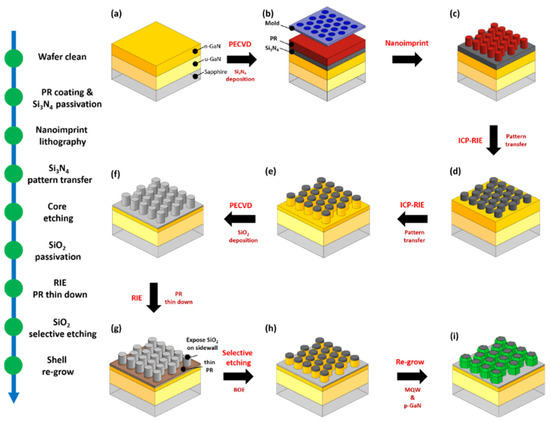
Figure 1.
Schematic process flow of 3D core–shell nanorod LED. (a) The epitaxial structure; (b) deposit Si3N4 on the n-GaN as passivation layer; (c) nanoimprint lithography process to produce a nanorod array; (d,e) transfer the pattern by SiO2 hard mask deposition; (f) deposit SiO2 and a thicker photoresist (PR) layer; (g) expose the SiO2 on the sidewalls of the nanorod; (h) selective removal of SiO2 on the sidewalls of the nanorod; (i) completed device.
The fabrication process flow begins with the growth of a 2.5 μm undoped GaN on a c-plane sapphire substrate by low-pressure metal organic chemical vapor deposition (MOCVD) followed by a 2 μm n-type GaN (n-type GaN, [Si] growth. The epitaxial structure is shown in Figure 1a. Secondly, Si3N4 is deposited on the n-GaN as the upper passivation layer, as shown in Figure 1b, and then the nanoimprint lithography process is applied to produce a nanorod array with a diameter of 650 nm, such as Figure 1c. The pattern is transferred by using inductively coupled plasma - reactive ionic etching (ICP-RIE). After the pattern is transferred twice, the 750 nm depth n-GaN core nanorod array is formed, as shown in Figure 1d,e. Subsequently, SiO2 and a thicker photoresist (PR) layer are deposited on top to cover the nanorod array in Figure 1f. After, the deposition, the thickness of PR is reduced and expose the SiO2 on the sidewalls of the nanorod, as shown in Figure 1g. In this way, the selective removal of SiO2 on the sidewalls of the nanorod was achieved by buffer oxide etching. After the wet etching, the bottom passivation layer is deposited, as shown in Figure 1h.
In the meantime, the single-passivated template (only the bottom SiO2 passivation layer) was also prepared. Finally, MOCVD was applied to grow high quality five pairs of InGaN/GaN multiple-quantum well (MQW), which is critical for a better device performance. Finally, p-GaN ([Mg]is then grown to finish the device process flow. The finished core–shell nanorod structure LEDs are shown in Figure 1i.
3. Results and Discussion
The surface energy and the stability of surface atoms are the two most important parameters influencing the growth rate of InGaN. The growth rate of InGaN on the Si3N4 layer is slower because of the passivation characteristic of nitrogen atoms. The top passivation layer on the double-passivated template effectively inhibits the formation of InGaN on the top of nanorods. As a result of reducing the area of the semipolar region and avoiding the formation of the tip structure, the thickness of the MQWs grown on the semipolar and nonpolar facets differs slightly. The thickness of InGaN and GaN grown on the semipolar facet are 2.5 nm and 7.5 nm, respectively, with a thickness of 3 nm and 8 nm, respectively, on nonpolar facets. The schematic diagram of the tip-free nanorod LED is shown in Figure 2a. We use a high-resolution transmission electron microscope (HRTEM) and SEM to examine the structure of nanorods, as shown in the inset of Figure 2b indicating the semipolar and nonpolar [] facets. The tip-free core–shell nanorod LED’s light–current–voltage (L-I-V) characteristics are shown in Figure 2c with a forward voltage of 3.15 V, and the maximum output power is 18.9 mW. Figure 2d shows the plot between external quantum efficiency (EQE) as a function of injection current exhibiting a maximum EQE value of 7.49%. Figure 2e shows the EL spectrum versus different driving current from 40 mA to 120 mA. Moreover, the peak wavelength shift exhibits a blue-shift from 517.9 nm (40 mA) to 505.8 nm (120 mA).
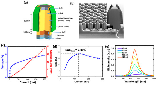
Figure 2.
(a) Schematic diagram of tip-free nanorod LED; (b) top-view SEM and TEM image of tip-free nanorod LED; (c) L-IV characteristics; (d) EQE value as a function of injection current; (e) EL spectrum versus different driving currents.
The polarization characteristics of two different nanorod LEDs are measured using a photoluminescence (PL) system. The energy band splits due to anisotropic epitaxial stress on the nonpolar and semipolar facets, and the intensity of different components in the emission light varies. This results in a specific polarization direction of the emission light, forming a polarized light source with the polarization measurement result shown in Figure 3a. The intensity of the emission light varies depending on the polarizer’s rotation angle, indicating that the light produced by the two devices has a specific degree of polarization and a polarization direction. Here, we define the degree of polarization (DOP, ρ) as
where I is the intensity of the light. The degree of polarization of tip-free and tip samples were found to be 0.545 and 0.188, respectively. The tip-free nanorod LED shows a higher degree of polarization due to the higher proportion of nonpolar MQWs emission. We established models based on the tip-free and tip nanorod LED and analyze the simulation results. We observed that there is no difference in the resonance mode between tip and tip-free samples since most of the energy is coupled in the nonpolar region, as shown in Figure 3b. The goal of this research is to produce a high polarized and efficient light source. As a result, the tip-free nanorod was chosen as the reference simulation model based on the polarization measurement. Seven different fundamental modes can be identified at the emission wavelength depending on the filling factor and the photonic crystal lattice constant of the device. Fourier transform on the energy distribution of these modes were applied in the near field to obtain the far field energy distribution. Then, Jones calculus was used to calculate the changes in the far field energy distribution after passing through the optical element. After passing through the polarizer with various rotation angles, the energy intensity of these modes is determined, and so the energy intensity of these modes can be estimated. Finally, the enhancement trend of the degree of polarization was observed, as shown in Figure 3c. The higher degree of polarization indicates the anisotropic energy distribution on the emission plane, or in other words, the higher intensity difference between the X direction and the Y direction. Therefore, the solved modes can be roughly divided into two types: the high symmetry mode and the low symmetry mode, which can be seen in Figure 3d,e. From the aspect of the mode characteristics, the mode with lower energy distribution symmetry enables for an enhanced degree of polarization. On the contrary, if the energy distribution of the modes is more symmetric, there is a relatively low enhancement in the degree of polarization.
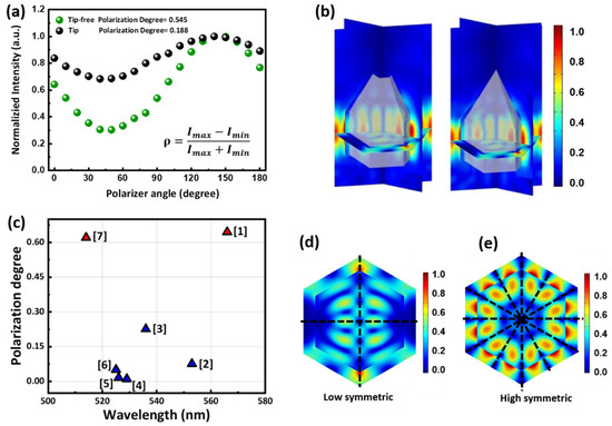
Figure 3.
(a) Polarization measurement result of tip and tip-free core–shell nanorod LED and (b) simulated mode profile in the tip and tip-free structure; (c) polarization enhances trend between different fundamental modes; (d,e) low symmetric mode profile and high symmetric mode profile.
Following that, we run a simulation of the divergence angle of the core–shell nanorod LED. Since the refractive index of GaN is higher than that of air, according to Snell’s law, the total internal reflection at the GaN/air interface causes part of the light to be confined within the nanorods, resulting in directional far field emission. We have proved this effect through the Finite-difference time-domain (FDTD) simulation of the nanorod array, as shown in Figure 4a. From the FDTD simulation, we observed that the height of the nanorod is related to the distance of the light confinement, as shown in Figure 4b. As the height of the nanorod increases, the effect of the light confinement becomes better. The result of the light field is shown in Figure 4c, and the effect of light confinement will saturate after a certain distance. There is no obvious influence if the height of the nanorod continues to increase after the saturation limit. The proposed GaN-based core–shell nanorod structure can reduce the divergence angle ranging from 120 degrees to 56 degrees, showing a directional far field emission. The calculated divergence angle results are summarized in Figure 4d showing reduction with increase in nanorod height.
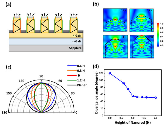
Figure 4.
(a) FDTD simulation of light confinement by core–shell nanorod structure; (b) simulation results of the light confinement effect by the nanorod structure at different heights (H = 980 nm); (c) light field pattern; (d) calculated divergence angle.
4. Conclusions
In summary, we investigated the characteristics difference between two different core–shell nanorod LEDs. The tip-free nanorod LED effectively inhibits the growth of MQWs on the semi-polar region and increases the area of nonpolar MQWs on the sidewalls of the nanorods by the top Si3N4 passivation layer. The higher degree of polarization from the tip-free nanorod LED indicates the higher ratio of nonpolar MQWs emission. Then, the effect of the light-coupling mode in the photonic crystal on the degree of polarization enhancement through numerical simulation was analyzed. Furthermore, the far field divergence angle is calculated through FDTD simulation. Due to the light confinement of the GaN nanorod, the divergence angle was reduced to 56 degrees. Using a 3D core–shell nanorod LED, a high degree of polarization, as well as a small divergence angle for backlight applications, can be achieved. This approach can be applied to a variety of different materials in the future to develop more efficient and novel optoelectronic devices.
Author Contributions
Conceptualization, K.-H.C.; methodology, K.-H.C.; software, K.-H.C.; validation, K.-H.C., J.-H.C., Y.-M.H. and K.-B.H.; formal analysis, J.-H.C. and S.-W.C.; investigation, K.-B.H.; resources, J.-H.C.; data curation, C.-W.S. (Chin-Wei Sher) and F.-Y.K.; writing—original draft preparation, C.-W.S. (Chin-Wei Sher); writing—review and editing, C.-W.S. (Chin-Wei Sher); visualization, C.-W.S. (Chia-Wei Sun); supervision, H.-C.K. and T.-S.K.; project administration, H.-C.K.; funding acquisition, H.-C.K. All authors have read and agreed to the published version of the manuscript.
Funding
This research received no external funding.
Institutional Review Board Statement
Not applicable.
Informed Consent Statement
Not applicable.
Data Availability Statement
Not applicable.
Acknowledgments
The authors express their gratitude to the Hon Hai Research Institute, HKUST, and FYTRI for their technical support and helpful discussion.
Conflicts of Interest
The authors declare no conflict of interest.
References
- Wu, Y.; Ma, J.; Su, P.; Zhang, L.; Xia, B. Full-Color Realization of Micro-LED Displays. Nanomaterials 2020, 10, 2482. [Google Scholar] [CrossRef] [PubMed]
- Paranjpe, A.; Montgomery, J.; Lee, S.M.; Morath, C. 45-2: Invited Paper: Micro-LED Displays: Key Manufacturing Challenges and Solutions. Soc. Inf. Disp. 2018, 49, 597–600. [Google Scholar] [CrossRef]
- Chen, Z.; Yan, S.; Danesh, C. MicroLED technologies and applications: Characteristics, fabrication, progress, and challenges. J. Phys. D Appl. Phys. 2021, 54, 123001. [Google Scholar] [CrossRef]
- Singh, K.J.; Fan, X.; Sadhu, A.S.; Lin, C.-H.; Liou, F.-J.; Wu, T.; Lu, Y.-J.; He, J.-H.; Chen, Z.; Wu, T.; et al. CsPbBr3 perovskite quantum-dot paper exhibiting a highest 3 dB bandwidth and realizing a flexible white-light system for visible-light communication. Photonics Res. 2021, 9, 2341–2350. [Google Scholar] [CrossRef]
- Chen, S.-W.H.; Huang, Y.-M.; Singh, K.J.; Hsu, Y.-C.; Liou, F.-J.; Song, J.; Choi, J.; Lee, P.-T.; Lin, C.-C.; Chen, Z.; et al. Full-color micro-LED display with high color stability using semipolar (20-21) InGaN LEDs and quantum-dot photoresist. Photonics Res. 2020, 8, 630–636. [Google Scholar] [CrossRef]
- Huang, Y.-M.; Chen, J.-H.; Liou, Y.-H.; James Singh, K.; Tsai, W.-C.; Han, J.; Lin, C.-J.; Kao, T.-S.; Lin, C.-C.; Chen, S.-C.; et al. High-Uniform and High-Efficient Color Conversion Nanoporous GaN-Based Micro-LED Display with Embedded Quantum Dots. Nanomaterials 2021, 11, 2696. [Google Scholar] [CrossRef] [PubMed]
- Jeong, Y.-C.; Lee, H.E.; Shin, A.; Kim, D.-G.; Lee, K.J.; Kim, D. Progress in Brain-Compatible Interfaces with Soft Nanomaterials. Adv. Mater. 2020, 32, 1907522. [Google Scholar] [CrossRef] [PubMed]
- Liu, Z.; Chong, W.C.; Wong, K.M.; Lau, K.M. GaN-based LED micro-displays for wearable applications. Microelectron. Eng. 2015, 148, 98–103. [Google Scholar] [CrossRef]
- Meng, W.; Xu, F.; Yu, Z.; Tao, T.; Shao, L.; Liu, L.; Li, T.; Wen, K.; Wang, J.; He, L.; et al. Three-dimensional monolithic micro-LED display driven by atomically thin transistor matrix. Nat. Nanotechnol. 2021, 16, 1231–1236. [Google Scholar] [CrossRef] [PubMed]
- Huang, Y.; Hsiang, E.-L.; Deng, M.-Y.; Wu, S.-T. Mini-LED, Micro-LED and OLED displays: Present status and future perspectives. Light Sci. Appl. 2020, 9, 105. [Google Scholar] [CrossRef] [PubMed]
- Lee, V.W.; Twu, N.; Kymissis, I. Micro-LED Technologies and Applications. Inf. Disp. 2016, 32, 16–23. [Google Scholar] [CrossRef]
- Huang, C.-H.; Cheng, Y.-T.; Tsao, Y.-C.; Liu, X.; Kuo, H.-C. Micro-LED backlight module by deep reinforcement learning and micro-macro-hybrid environment control agent. Photonics Res. 2022, 10, 269–279. [Google Scholar] [CrossRef]
- Pan, A.; Zhou, Y.; Zhao, C.; Shi, C.; Wu, Y.; Zhang, Y.; Liu, Y.; He, L. Luminescent and ultrastable perovskite-acrylate based elastomers with excellent stretchability and self-healing capability for flexible backlight display. Chem. Eng. J. 2022, 433, 133590. [Google Scholar] [CrossRef]
- He, C.-L.; Liang, F.-C.; Veeramuthu, L.; Cho, C.-J.; Benas, J.-S.; Tzeng, Y.-R.; Tseng, Y.-L.; Chen, W.-C.; Rwei, A.; Kuo, C.-C. Super Tough and Spontaneous Water-Assisted Autonomous Self-Healing Elastomer for Underwater Wearable Electronics. Adv. Sci. 2021, 8, 2102275. [Google Scholar] [CrossRef] [PubMed]
- Yang, G.; Zhong, H. Multi-Dimensional Quantum Nanostructures with Polarization Properties for Display Applications. Isr. J. Chem. 2019, 59, 639–648. [Google Scholar] [CrossRef] [Green Version]
- Yang, D.K. Review of operating principle and performance of polarizer-free reflective liquid-crystal displays. J. Soc. Inf. Disp. 2008, 16, 117–124. [Google Scholar] [CrossRef]
- Weder, C.; Sarwa, C.; Montali, A.; Bastiaansen, C.; Smith, P. Incorporation of photoluminescent polarizers into liquid crystal displays. Science 1998, 279, 835–837. [Google Scholar] [CrossRef]
- Yuan, Y.; Fan, F.; Zhao, C.; Kwok, H.-S.; Schadt, M. Low-driving-voltage, polarizer-free, scattering-controllable liquid crystal device based on randomly patterned photo-alignment. Opt. Lett. 2020, 45, 3697–3700. [Google Scholar] [CrossRef] [PubMed]
- Feezell, D.F.; Schmidt, M.C.; DenBaars, S.P.; Nakamura, S. Development of nonpolar and semipolar InGaN/GaN visible light-emitting diodes. MRS Bull. 2009, 34, 318–323. [Google Scholar] [CrossRef]
- Zhao, Y.; Tanaka, S.; Yan, Q.; Huang, C.-Y.; Chung, R.B.; Pan, C.-C.; Fujito, K.; Feezell, D.; Van de Walle, C.G.; Speck, J.S. High optical polarization ratio from semipolar (20 ) blue-green InGaN/GaN light-emitting diodes. Appl. Phys. Lett. 2011, 99, 051109. [Google Scholar] [CrossRef]
- Crawford, M.H. LEDs for solid-state lighting: Performance challenges and recent advances. IEEE J. Sel. Top. Quantum Electron. 2009, 15, 1028–1040. [Google Scholar] [CrossRef]
- Pimputkar, S.; Speck, J.S.; DenBaars, S.P.; Nakamura, S. Prospects for LED lighting. Nat. Photonics 2009, 3, 180–182. [Google Scholar] [CrossRef]
- Weisbuch, C.; Piccardo, M.; Martinelli, L.; Iveland, J.; Peretti, J.; Speck, J.S. The efficiency challenge of nitride light-emitting diodes for lighting. Phys. Status Solidi A 2015, 212, 899–913. [Google Scholar] [CrossRef]
- Mukai, T.; Yamada, M.; Nakamura, S. Current and temperature dependences of electroluminescence of InGaN-based UV/blue/green light-emitting diodes. Jpn. J. Appl. Phys. 1998, 37, L1358. [Google Scholar] [CrossRef]
- Zhang, H.; Li, P.; Li, H.; Song, J.; Nakamura, S.; DenBaars, S.P. High polarization and fast modulation speed of dual wavelengths electroluminescence from semipolar (20-21) micro light-emitting diodes with indium tin oxide surface grating. Appl. Phys. Lett. 2020, 117, 181105. [Google Scholar] [CrossRef]
- Kishino, K.; Sakakibara, N.; Narita, K.; Oto, T. Two-dimensional multicolor (RGBY) integrated nanocolumn micro-LEDs as a fundamental technology of micro-LED display. Appl. Phys. Express 2019, 13, 014003. [Google Scholar] [CrossRef]
- Masui, H.; Nakamura, S.; DenBaars, S.P.; Mishra, U.K. Nonpolar and semipolar III-nitride light-emitting diodes: Achievements and challenges. IEEE Trans. Electron Devices 2009, 57, 88–100. [Google Scholar] [CrossRef]
- Monavarian, M.; Rashidi, A.; Feezell, D. A Decade of Nonpolar and Semipolar III-Nitrides: A Review of Successes and Challenges. Phys. Status Solidi A 2019, 216, 1800628. [Google Scholar] [CrossRef] [Green Version]
- Riley, J.R.; Padalkar, S.; Li, Q.; Lu, P.; Koleske, D.D.; Wierer, J.J.; Wang, G.T.; Lauhon, L.J. Three-dimensional mapping of quantum wells in a GaN/InGaN core–shell nanowire light-emitting diode array. Nano Lett. 2013, 13, 4317–4325. [Google Scholar] [CrossRef]
- Tzou, A.-J.; Hsieh, D.-H.; Hong, K.-B.; Lin, D.-W.; Huang, J.-K.; Chen, T.-P.; Kao, T.-S.; Chen, Y.-F.; Lu, T.-C.; Chen, C.-H. High-efficiency InGaN/GaN core–shell nanorod light-emitting diodes with low-peak blueshift and efficiency droop. IEEE Trans. Nanotechnol. 2016, 16, 355–358. [Google Scholar] [CrossRef]
- Ke, M.-Y.; Wang, C.-Y.; Chen, L.-Y.; Chen, H.-H.; Chiang, H.-L.; Cheng, Y.-W.; Hsieh, M.-Y.; Chen, C.-P.; Huang, J. Application of nanosphere lithography to LED surface texturing and to the fabrication of nanorod LED arrays. IEEE J. Sel. Top. Quantum Electron. 2009, 15, 1242–1249. [Google Scholar]
Publisher’s Note: MDPI stays neutral with regard to jurisdictional claims in published maps and institutional affiliations. |
© 2022 by the authors. Licensee MDPI, Basel, Switzerland. This article is an open access article distributed under the terms and conditions of the Creative Commons Attribution (CC BY) license (https://creativecommons.org/licenses/by/4.0/).