Article

Scalable and Blue Photoluminescence Emissions of (C4H9NH3)2PbBr4 2D Perovskite Fabricated by the Dip-Coating Method Using a Co-Solvent System

1
Division of Pediatric Surgery, Department of Surgery, Taichung Veterans General Hospital, Taichung 40705, Taiwan
2
Department of Medicine, National Yang Ming Chiao Tung University, Taipei 112, Taiwan
3
Department of Medical Applied Chemistry, Chung Shan Medical University, Taichung 40201, Taiwan
4
Department of Applied Materials and Optoelectronic Engineering, National Chi Nan University, Nantou 54561, Taiwan
5
Department of Medical Education, Chung Shan Medical University Hospital, Taichung 40201, Taiwan
*
Authors to whom correspondence should be addressed.
Crystals 2022, 12(3), 418; https://doi.org/10.3390/cryst12030418
Submission received: 26 February 2022 / Revised: 7 March 2022 / Accepted: 13 March 2022 / Published: 18 March 2022

Abstract

:
The improved efficiency of perovskite-related photovoltaic devices, such as light-emitting diodes (LEDs), is related to film uniformity, the compactness of each layer, and thickness. Herein, we improved the traditional single-solvent, solution-processed method and developed a co-solvent method to prepare a two-dimensional (2D) (C4H9NH3)2PbBr4 perovskite film for blue photoluminescence (PL) emissions. A poor film-forming uniformity was observed for the use of the single-solvent, dimethylformamide (DMF) method. In adding 1,2-dichlorobenzene (ODCB) of a smaller polarity to DMF, the co-solvent engineering dramatically changed the film-forming properties. Optical microscopy (OM), scanning electron microscopy (SEM), X-ray diffractometer (XRD), and time-resolved PL (TR-PL) spectroscopy analyses confirmed that the perovskite film prepared by the co-solvent system had a good crystallinity, fewer defects, and a longer carrier lifetime. These experimental results show a simple, scalable (1.23 × 1.23 cm2), and stable reproducibility method for preparing 2D perovskite of 415 nm wavelength PL emissions that might be beneficial for the development of ultraviolet (UV) photodetectors, blue LEDs, and high-resolution displays.

1. Introduction

Two-dimensional (2D) materials have received interest in academic research due to the continuous advancement of transistor technology, in the course of which the size of transistors has been continuously reduced to satisfy the requirements of light-weight and compact electronic devices [1]. However, the reduced size of transistors may possibly cause a short tunneling effect, which increases the leakage current and further increases power consumption or generates heat. Therefore, many researchers have put a great deal of effort into solving this problem [2]. There are two common solutions: one is to increase the gating control of the channel and reduce the influence of the electric field from the drain on the channel. Therefore, the shape of the transistor changes from the traditional planar bulk field-effect transistor (FET) to a three-dimensional (3D) Fin-FET [3]. In addition to the development of a 3D structure, another possible solution is to remove the part of the channel that is more susceptible to the influence of the drain electric field—that is, the part of the channel that is far from the gate. As the gate length shrinks, the thickness of the silicon channel needs to be reduced correspondingly [4]. Since the channel thickness is close to zero, theoretically, the gate could completely control the channel and suppress the electric field caused by the drain, minimizing the short channel effect and any leakage current. Therefore, the ideal 2D FET could be considered the perfect transistor [5].
In the study of 2D materials, planar perovskite films of excellent charge carrier mobility have been shown to be suitable in the use of FETs [6]. In addition to not requiring high-temperature production, perovskite-based photovoltaics have reached a conversion efficiency of more than 20% in just a few years, and the speed of research progress is quite amazing [7]. The advantages of perovskite materials include fast carrier transmission, a tunable light absorption range, a narrow energy gap, and a low cost. The operating principle of perovskite-based photovoltaics is similar to that of p-n junction devices, and recent research has focused on the modification and synthesis of the material itself, or on carrier transport and electrode materials [8].
Perovskite materials first appeared in dye-sensitized solar cells (DSSCs), and were later used in light-emitting diodes (LEDs) [7]. The initial simple device structure, electrode/perovskite/electrode, full of an organic electrolyte solution, used two photosensitizers (CH3NH3PbBr3 and CH3NH3PbI3), and their efficiency was 3.13% and 3.81%, respectively [9]. Scientists have found that perovskite materials themselves have the characteristics of being able to adjust the energy band gap and the low non-radiation recombination rate. The widely studied 3D methylammonium lead iodide (MAPbI3) perovskite is commonly integrated into perovskite-based photovoltaics; however, the issue of stability severely inhibits the development of its commercial use [10]. On the contrary, 2D thin-layered perovskite ((CnH2n + 1NH3)2PbX4, X = Br or I, n ≥ 4), with a longer hydrophobic alkyl chain and weaker polarity, has been proven to increase stability for solar cell applications in a humid environment [11]. In addition, 2D perovskite films have an excellent charge carrier mobility [12] and high photovoltaic efficiency in solar cells [13]. Even though, in recent years, great progress has been made in the development of 2D perovskite materials, achieving a scalable, large-area, thin film combined with simple solution processing is still a challenge [14,15,16,17,18]. The efficiency of perovskite-based photovoltaics is related to the uniformity, compactness, coverage, and thickness of the structure, which are all related to the organic–inorganic lattice arrangement determined by the fabrication process.
For solution-processed perovskite, solvents play an important role in the crystallization of films. A typical spin-coating method has been applied to fabricate perovskite films under different solvent conditions [19], showing two mixed phases of tetragonal + cubic with a small amount of precipitated PbI2 after annealing. These different solvent conditions affect the flatness and coverage of the surface morphology of the perovskite. Three solvent methods, chlorobenzene/dimethylacetamide/acetonitrile, have been used to control the formation of 2D perovskite. Two-dimensional perovskite, (C4H9NH3)2PbBr4, of an ultrathin and lateral dimension of up to 40 μm, was synthesized with a good reproducibility [20]. It has been found that polar solvents, such as acetonitrile, contribute to the formation of ultra-thin structures [21]. According to the previously reported research, the solvent volume ratio, crystallization temperature, and solvent polarity have a certain relationship with the morphology and crystallization of thin perovskite films. Therefore, in this study, we used a co-solvent engineering system to synthesize 2D perovskite films by adjusting the polarity and dielectric constant of one solvent using a fixed, commonly used solvent, DMF. The XRD of the fabricated perovskite proved the 2D structure, (C4H9NH3)2PbBr4, of blue photoluminescence (PL) emissions, which could possibly be used in UV photodetectors or LEDs.

2. Materials and Methods

Glass substrates were prepared at a size of 1.23 × 1.23 cm2. All of the glass substrates were cleaned using ultrasonic vibration for 10 min with methanol and acetone, separately. The dried substrates were placed into an oxygen plasma cleaner to remove the remaining dirt and to create a hydrophilic surface. For the preparation of the perovskite material, a single or co-solvent engineering system was used. All solution preparations used for growing a perovskite film were carried out under ambient conditions in the fume hood. For the preparation of 3D perovskite, lead (Ⅱ) bromide (PbBr2, 0.0324 g) and methylammonium bromide (MABr, 0.0224 g) were first dissolved in 4 mL of dimethylformamide (DMF) solution, separately. The mixed solution (MABr and PbBr2) at a 2:1 molar concentration was then mixed with different solvents at a 1:1 volume ratio. The fabrication of 2D perovskite was performed in a similar way, where the MABr was replaced by n-butylammonium bromide (BABr). All chemicals were purchased from Merck, Taipei, Taiwan (Sigma-Aldrich). A total volume of 0.16 mL of the transparent mixed solution was taken and slowly dropped onto a glass substrate heated under different temperatures and at a fixed time of 2.5 h to obtain an opaque, white perovskite film. Additional light exposure was used under a 100 mW UV LED or 5 W white LED light source. A JSM-7800F field emission scanning electron microscope (FE-SEM) manufactured by JEOL was used to observe the surface and cross-sectional morphology of the perovskite film. An X-ray thin-film diffractometer (Bruker AXS Gmbh, Karlsruhe, Germany), using a copper target as the X-ray light source (Cu-Kα; λ = 0.154 nm), was used to analyze the X-ray diffraction (XRD) pattern of the thin perovskite film. The diffraction angle scanned in this experiment was 5–60° for a single-layer film, and the scanning speed was 5°/min. Time-correlated single photon counting (TCSPC; PicoQuant, Berlin, Germany) was used to measure the time-resolved fluorescence spectrum of the sample. The working principle of TCSPC is that the sample is first excited by a periodic pulsed laser light source (PDL 800-B diode laser, 375 nm) and fluorescent photons are generated. The time point of the generated photon was detected and recorded by the photomultiplier tube (PMT) via a single photon measurement method, and this time point was used as the start point. The system then recorded the time point of the photon triggered by a laser as the end point. Since the laser signal interval was a known, fixed value, the system could accumulate fluorescent photon signals generated at different times. The Raman spectrum was recorded using a 30 mW He-Ne laser as the excited light source and a Horiba Jobin Yvon IHR320 spectrometer at an accumulated time of 30 s.

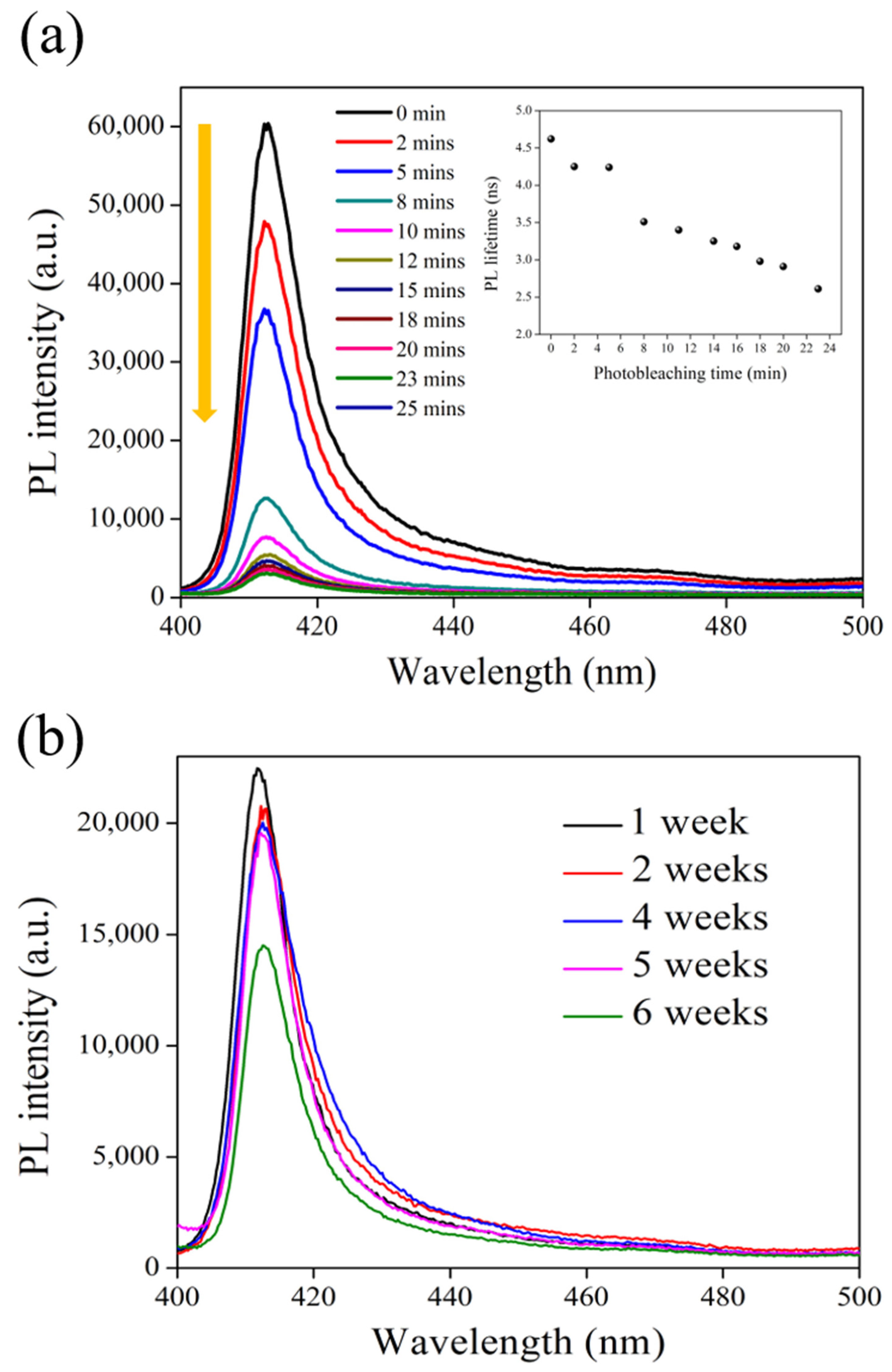
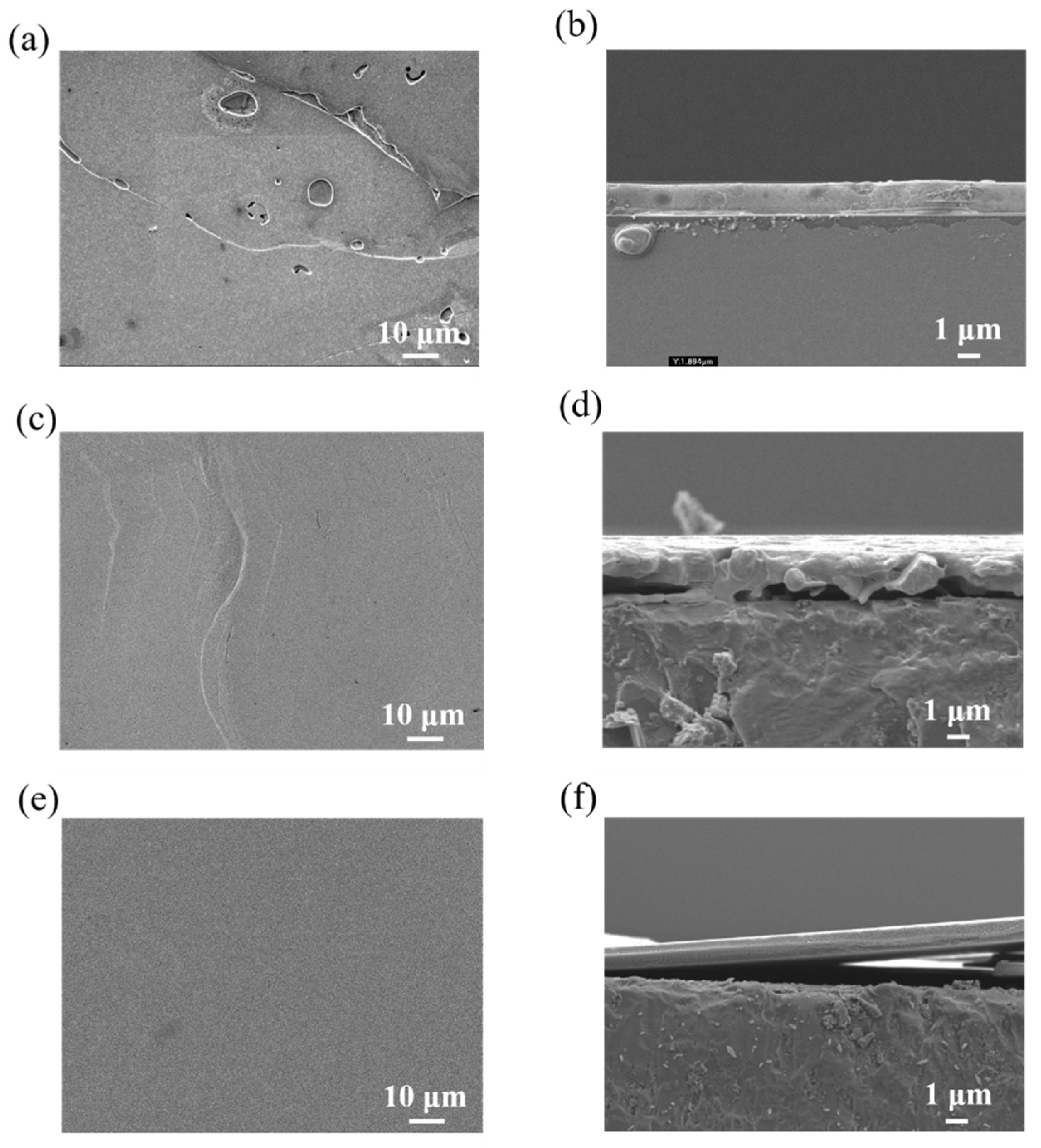
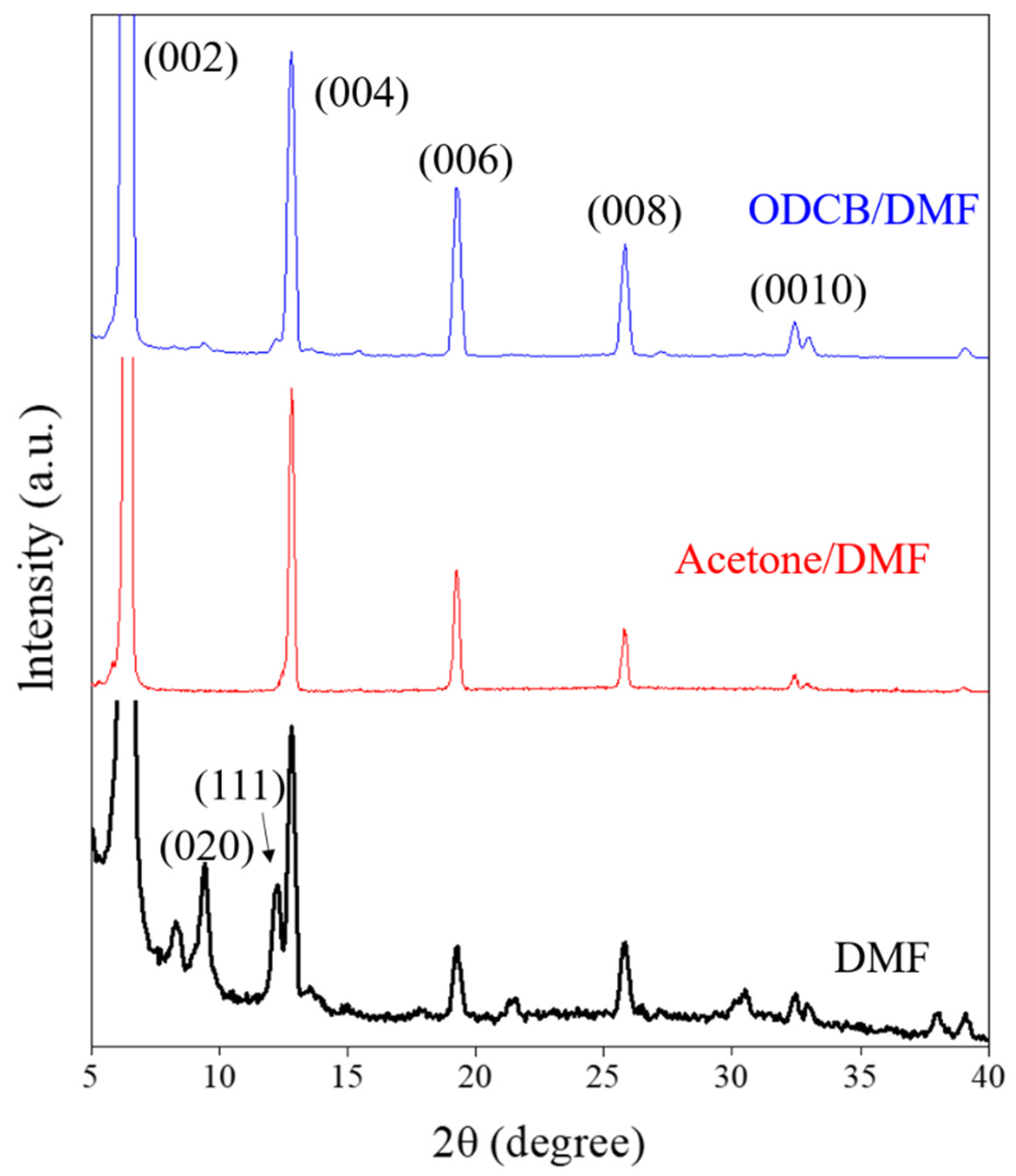
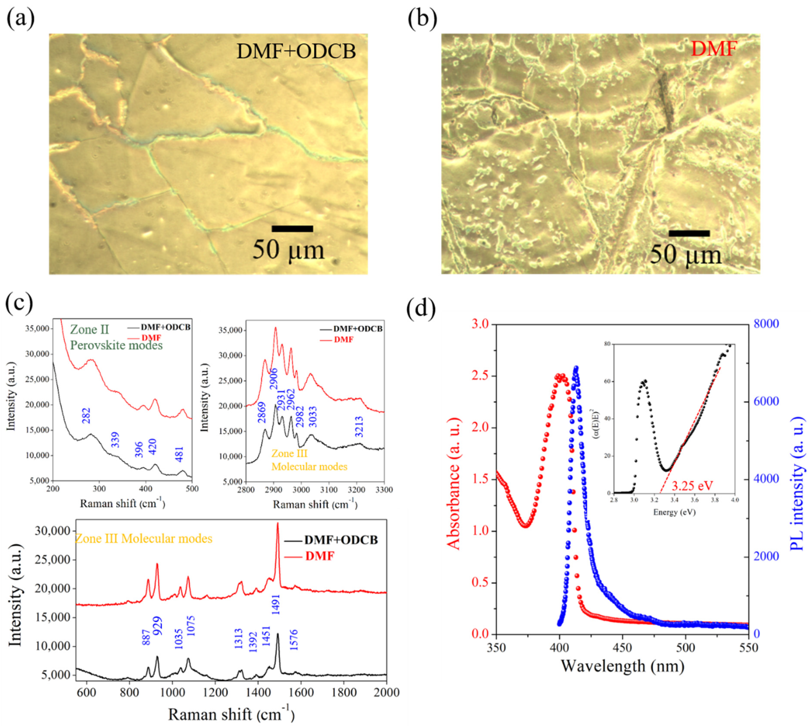
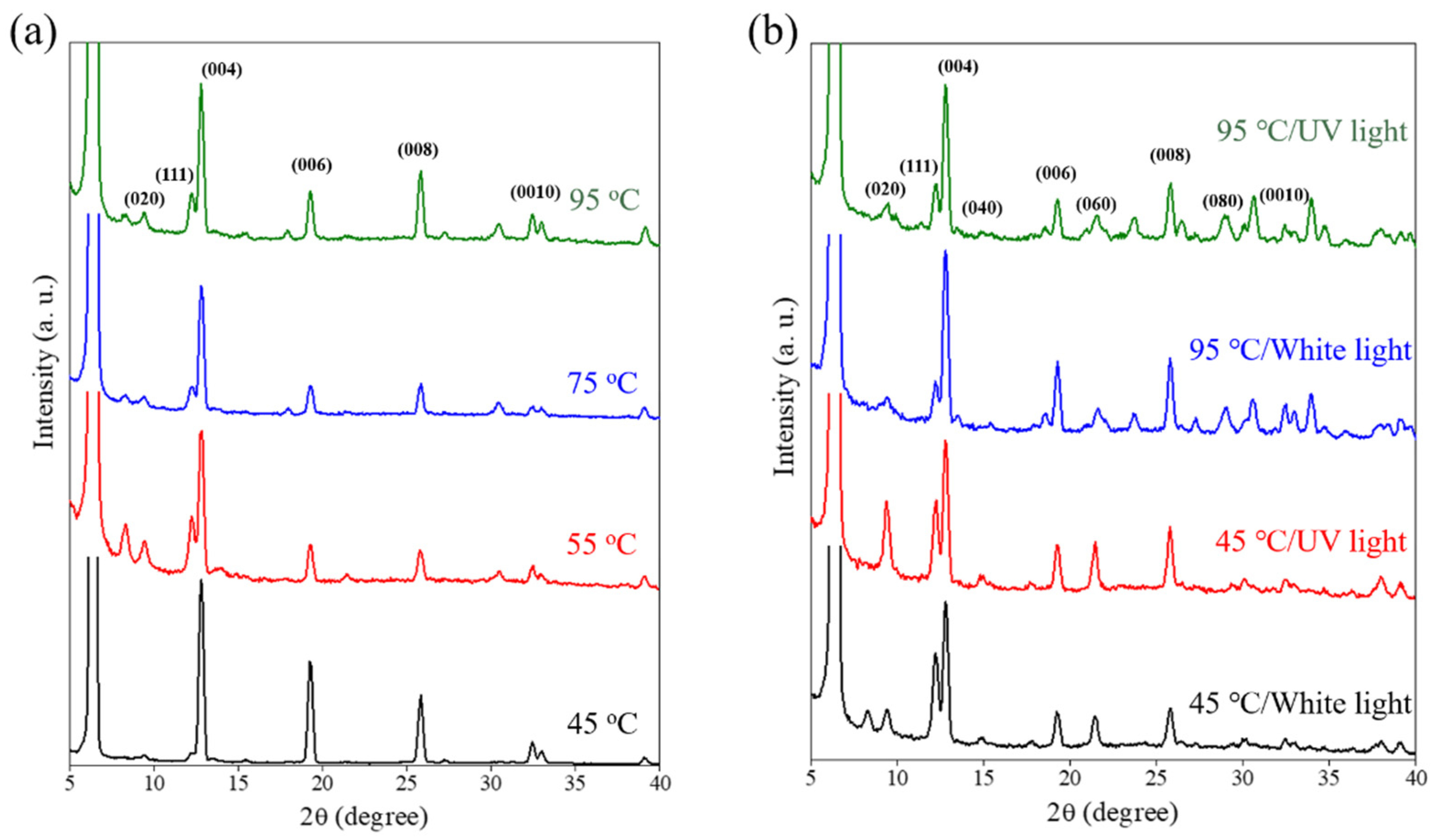
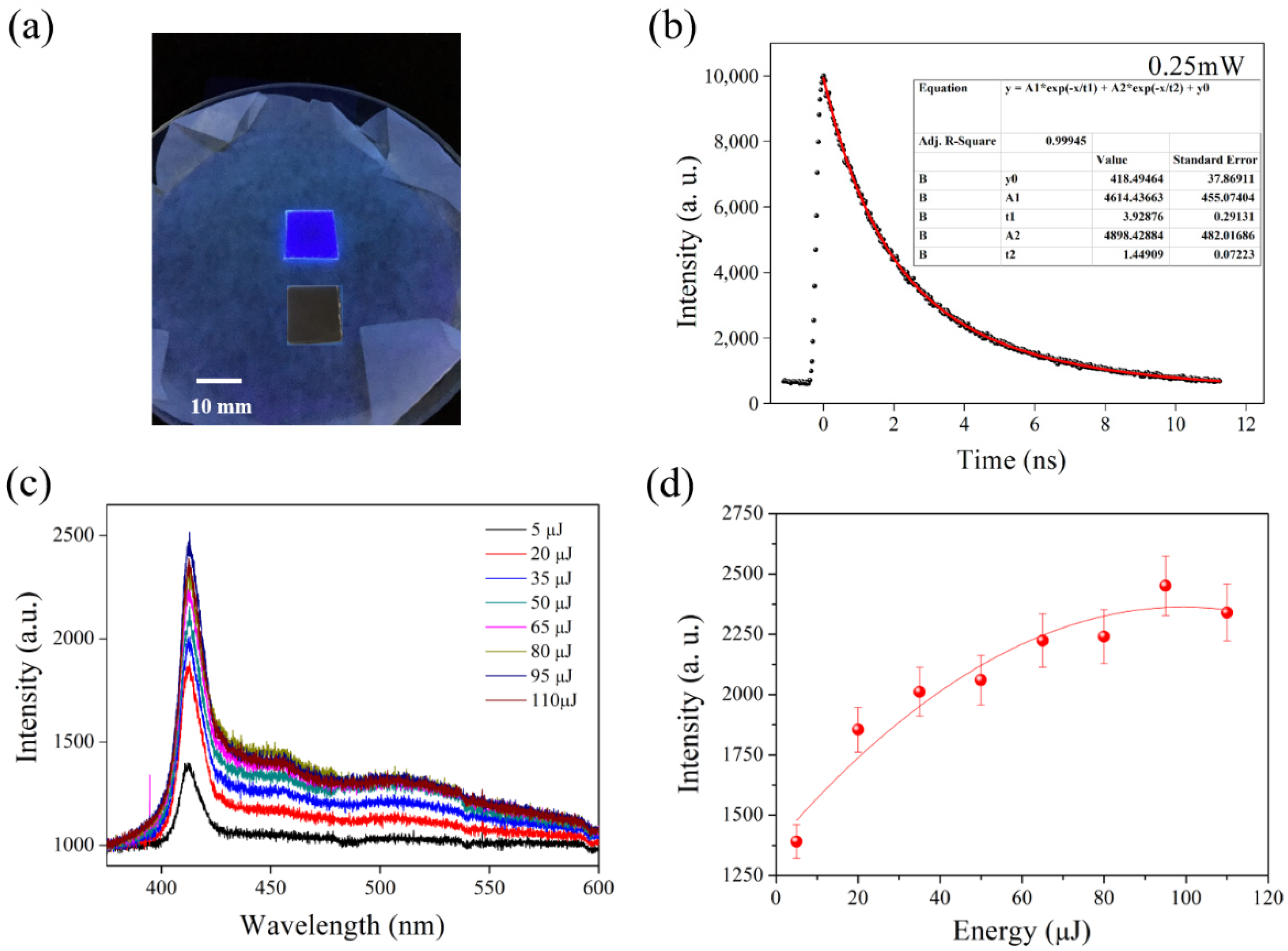
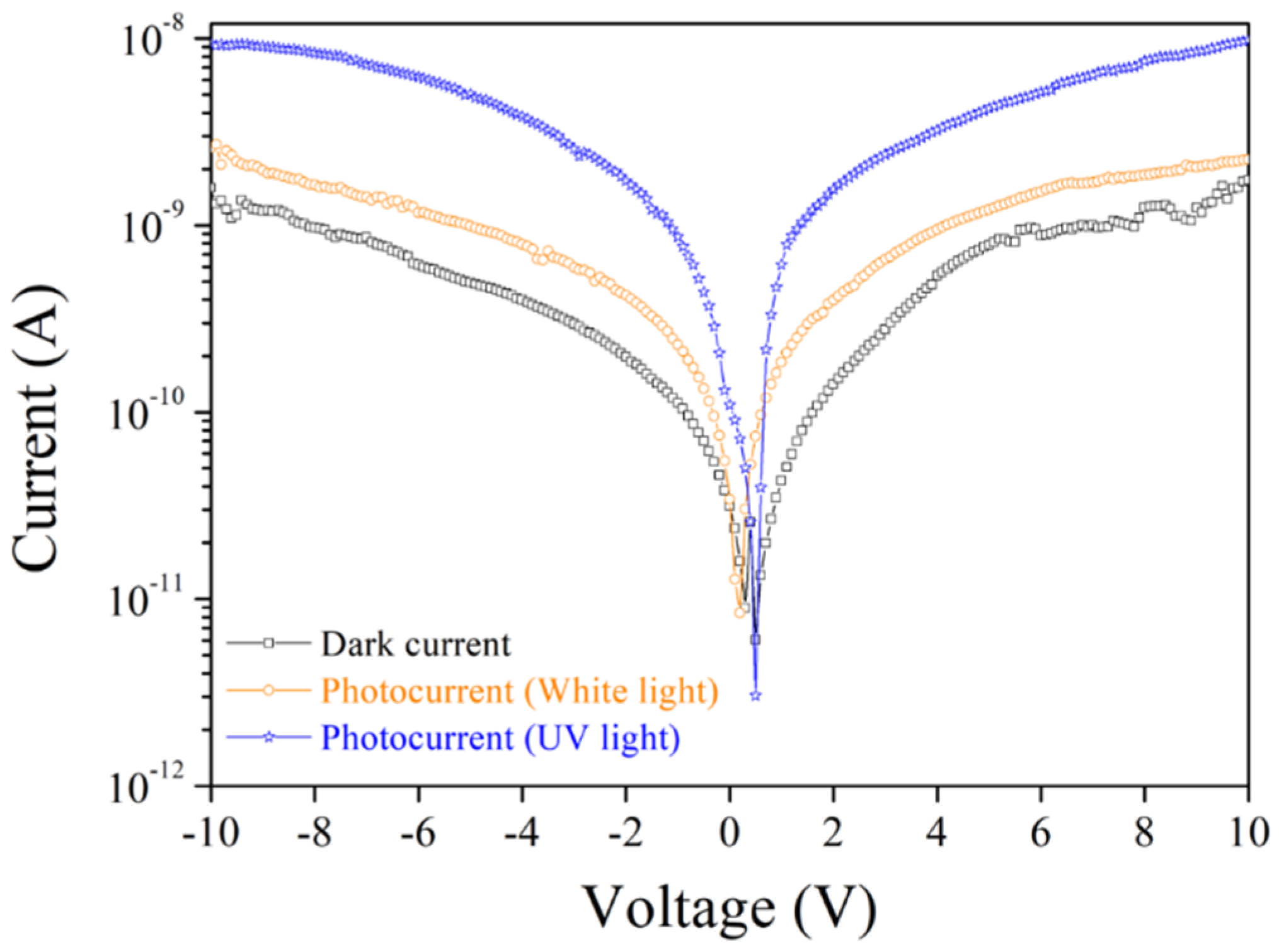
3. Results and Discussion

Previous reports of using three solvent systems to fabricate single- and multilayer 2D perovskite [21] have shown that the supersaturation and the crystallization temperature of the perovskite precursor are the two main factors affecting the final morphology of the perovskite film. For the co-solvent system, several solvents have been used in the preparation of perovskite materials [22], especially the use of chlorobenzene (CB) as a secondary solvent (second solvent) added to the commonly used DMF (primary solvent). The growth mechanism of perovskite in a diluted solution with a DMF ratio of 14.3–25% could be a contribution of the diffusion due to the uneven supersaturation at the interface between the two solvents [23]. In addition, the use of acetonitrile (ACN) in the second step of synthesis results in the supersaturation of the solution increasing unilaterally. The growth mechanism changes from diffusion control to inertial control, which leads to the evolution of the morphology. Using CB as the solvent ensures the inhibition of crystallization, and ACN helps to improve the phenomenon of uneven supersaturation and promotes the 2D crystal growth. Previous reports on co-solvent systems have concluded that the mixed solvent method more easily produces perovskite films with an area of up to 40 μm in size; in particular, polar solvents, such as ACN and alcohols, are considered to be useful in helping to grow 2D perovskite [24,25]. The common solvents with different polarities and dielectric constants are shown in Table 1.
To evaluate the effect of adding a second solvent on the crystalline growth of perovskite, we first evaluated the crystalline growth of 3D perovskite fabricated by a DMF-based co-solvent system using SEM images, as shown in Figure 1. Since the reactants MABr and PbBr2 used for fabricating 3D perovskite need to be dissolved in a non-polar solvent, the use of a solvent of higher polarity, such as formamide, could cause the non-dissolution of the precursors, and the mixed solution showed suspended particles which were slightly yellow in color. DMF was used as the primary solvent because of its good solubility and for having many perovskite precursors. There were many different options for the second solvent, such as acetone, isopropyl alcohol (IPA), o-dichlorobenzene (ODCB), and dimethyl sulfoxide (DMSO). We simply mixed MABr and PbBr2 at a 2:1 molar ratio in a co-solvent system with a 1:1 volume ratio by adding four different solvents (acetone, IPA, DMSO, and ODCB) into the DMF solution. For the case of using acetone and IPA as the second solvent, since both solvents have similar dielectric constants, the surface morphology should be similar; however, the sample using acetone as the second solvent showed more crystalline growth, as shown in Figure 1a. This may be attributed to the higher evaporation rate of acetone due to its lower boiling point temperature. For the case of using DMSO and ODCB as the second solvents, since both solvents have similar boiling points, the surface morphology should be similar; however, less crystalline growth was observed in the case of using ODCB as the second solvent, as shown in Figure 1d.
For the fabrication of 2D perovskite, we first tried to use a single solvent, DMF, to fabricate a 2D perovskite film 1.23 × 1.23 cm2 in size using the dip-coating method, in which BABr and PbBr2 were used as precursors. Figure 2 shows surface and cross-sectional SEM images and the XRD pattern of the fabricated films. The surface morphology of the 2D perovskite film obtained by simply dissolving precursors in DMF (single solvent) not only had narrow and long gaps, but also had some defect holes, as shown in Figure 2a, which are not favorable for the light energy conversion efficiency for photovoltaic applications [26]. DMSO, which has a dielectric constant close to that of DMF, was then used as the second solvent in the DMF-based co-solvent system. DMSO and DMF were mixed homogeneously and yielded a transparent mixing solution. However, the boiling point of DMSO is comparably high, which means that it took at least four hours to fabricate the perovskite film at a controlled temperature of 45 °C. Moreover, the film surface showed uneven crystal grains that could be observed with the naked eye. Figure 2c shows the surface morphology of the 2D perovskite film fabricated by the acetone/DMF co-solvent system, showing a better surface morphology. However, the cross-sectional image indicates inhomogeneous crystalline growth, as shown in Figure 2d. The best candidate was using ODCB, which has a similar boiling point to DMSO, as the second solvent. It took 2.5 h to fabricate a thin perovskite film using ODCB, less than when using DMSO. It is speculated that the differences in the dielectric constant of the solvent itself cause different drying times. Figure 2e,f show surface and cross-sectional images of the 2D perovskite film fabricated by the ODCB/DMF co-solvent system. Not only does the surface morphology indicate a homogeneous 2D crystalline structure 2 μm in thickness, but so do the cross-sectional images.
For the XRD analysis, the peaks at 6.4°, 13.2°, 19.4°, 26.3°, and 33.7° correspond to the (002), (004), (006), (008), and (0010) crystal planes, respectively, indicating the existence of a 2D perovskite structure [27,28]. However, other plane directions, such as (020) and (111), also appeared in the 2D perovskite film fabricated by a single solvent (DMF), as represented by the black peaks in Figure 3. Other peaks located at 8.3°, 21.4°, and 30.5° might belong to other planes, such as (111), (020), or (202), due to the complete transformation of a metal organic framework (MOF) structure under evaporation and crystalline processes following long-term annealing treatment [29,30]. However, these peaks were not observed in the co-solvent system, acetone/DMF and ODCB/DMF, as represented by the red and blue peaks in Figure 3. Those characteristic XRD peaks, proving that the crystalline structure of the fabricated 2D perovskite was (C4H9NH3)2PbBr4 [31]. It is obvious that the peak intensities of those 2D planes were comparably higher in the co-solvent fabricated perovskite, and especially that the long-range ordering was increased in the 2D perovskite film fabricated by the ODCB/DMF co-solvent system.
Compared to the single solvent system, the use of a co-solvent or an anti-solvent (acetone or ODCB) yielded a porous surface with grains smaller than 100 nm, as shown in Figure 4a (surface) and Figure 4b (cross-sectional). The porous structure may be ascribed to the change in the slow crystallization process due to the addition of an anti-solvent with a higher boiling point.
The use of an optical microscope (OM) to characterize the surface morphology of perovskite films provides better information on films of large areas. Figure 5a,b compare the two cases, showing that, under co-solvent conditions, the film had a crystalline structure area of 100 μm2 in size, with a long and narrow grain boundary. However, the perovskite film made using the single solvent system showed numerous point and line defects. A comparison of the Raman spectra characterized from single- and co-solvent-fabricated 2D perovskite is shown in Figure 5c. These Raman spectra were obtained by irradiating laser excitation at 633 nm on a specimen focused by an optical microscope. The vibration modes of 2D perovskite in the low Raman band (15 to 150 cm−1) could provide a wealth of information on the crystalline structure [32]. Moreover, a theoretical calculation using density functional theory showed that the Raman spectrum of lead halide perovskite could be separated into two zones: perovskite mode in the Raman band of 200–500 cm−1 and molecular mode in the Raman band of 500–3550 cm−1. The Raman spectra of the 2D perovskite fabricated using either a single solvent or a co-solvent all had characteristic Raman peaks belonging to CH3NH3Br. When n-butyl+ was embedded in PbBr2, a chemical Stark effect occurred [33]. There were sharp and distinct bands from C–H stretching and CH3+ asymmetric bending in the molecular mode in the Raman band from 887 to 1491 cm−1, as shown in Figure 5c. These peaks were significantly red-shifted compared to the PbBr2 powder sample, indicating that the 2D perovskite of MOF had strong interactions [34]. In the higher Raman band region, νsym (CH3) at 2869 cm−1 and νsym (CH3) at 2931 cm−1 were not displaced after embedding n-butyl+, while νsym (C–H) at 2906 cm−1 was blue-shifted. The broad νsym (CH3+) of 3033 cm−1 exhibited red- or blue-shifting compared to the PbBr2 powder [33]. In other words, organic cations and inorganic skeletons occurred through the CH3+ end of n-butyl+. The decomposition of νsym (CH3+) at 3033 cm−1 was most likely due to the binding of the halide to the hydrogen bond in the form of C–H···Br. Figure 5d shows the optical absorption and photoluminescence (PL) spectrum for the (C4H9NH3)2PbBr4 2D perovskite film fabricated by a co-solvent (DMF+ODCB) solution processing method. Both the absorption and the PL spectrum showed a sharp peak with a Lorentzian line shape located at 400 and 410 nm, respectively. A relatively small bandwidth was observed in both the absorption and the PL spectra, indicating a characteristic of free excitation, while the broad PL peak located at 440 nm was attributed to self-tapped excitation [35]. Figure 5d (inset) shows the Tauc plot, indicating that the bandgap of the fabricated 2D perovskite was 3.25 eV.
Figure 6 compares the XRD of the 2D perovskite fabricated by the ODCB/DMF co-solvent system under different heating temperatures and light exposures. Previous studies have proven that a lower annealing temperature facilitates a larger grain size for a perovskite film [26]. Our experimental results showed that a higher annealing temperature helps the growth of a crystalline structure of the (111) and (020) planes, as shown in Figure 6a. Those peaks also appeared in the perovskite fabricated by single solvent (DMF), as shown in Figure 3. Those peaks might be attributed to the emergence of (111) and (020), indicating a disorientation of the thin film, and a non-orderly stacking of 2D platelets due to the higher temperature. Previous studies have shown an effective way of changing the crystallization mechanism of a perovskite film, in which light could reduce the critical nucleus size [36,37]. Herein, we tried to use UV and white light to modulate the crystalline growth of 2D perovskite and observed that UV and white light exposure help the growth of the (020) and (111) planes. Our findings could possibly be used to improve the photovoltaic efficiency of 2D perovskite films.
The direct observation of PL emissions from 2D perovskite films was achieved by taking photographs of the glass substrate without and with the growing film on top, as shown in Figure 7a. Homogeneous PL emissions with a large area substrate (1.23 × 1.23 cm2) of the fabricated 2D perovskite film could possibly offer a way to approach scalable, true blue, organic LEDs. The PL lifetime of fabricated (C4H9NH3)2PbBr4 2D perovskite was measured using the TCSPC method, for which a 375 nm picosecond laser wavelength was used for excitation, as shown in Figure 7b. The decay curve showed a bi-exponential feature with lifetimes of 1.45 and 3.93 ns. The PL properties of the 2D perovskite film was further studied by performing an additional excitation power-dependent PL measurement at room temperature, as shown in Figure 7c. An additional PL peak located at 460 nm and a PL shoulder of a longer wavelength appeared when the 2D perovskite film was under higher-energy laser irradiation. No obvious shift in the PL peak indicates a 2D perovskite film of a larger grain size [38]. The evolution of PL intensity dependent on pumping laser energy is shown in Figure 7d. The saturated PL intensity may be attributed to hot carrier recombination with excited donors and acceptors at higher energy levels [38].
In order to study the photostability of 2D perovskite, the real-time monitoring of the PL intensity and lifetime was carried out over a 30 min time frame, as shown in Figure 8a. The expected degradation of the PL intensity was observed due to the generation of defects under light irradiation [39]; however, the PL lifetime was only slightly decreased from 4.5 to 2.5 ns. Figure 8b shows the spectra of PL intensity recorded in a weekly time frame, in which the photostability of 2D perovskite remained stable in the first five weeks and suddenly decreased in the sixth week.
Finally, we tried to understand the photodetecting behavior of the fabricated (C4H9NH3)2PbBr4 2D perovskite film. The current and voltage (I–V) behaviors of 2D perovskite under different light environments were observed through a simple metal–semiconductor–metal (MSM) design, and the results are shown in Figure 9. Because the absorption spectrum of this 2D perovskite was in the UV wavelength range, as shown in Figure 5d, the photocurrent under the I–V measurement, compared to the dark current, was observed to increase obviously under UV light irradiation compared to white light illumination. The photocurrent of 2D perovskite increased by one order of magnitude compared to the dark current under UV light irradiation.

4. Conclusions

We tried to control the supersaturation and crystallization temperature for fabricating 2D perovskite and analyzed its surface morphology, crystalline structure, and emission properties. OM and SEM images were used to directly verify that a low temperature of 45 °C was the better crystalline temperature for growing 2D perovskite with uniformity and a single crystal of a large grain size. The XRD confirmed the crystalline structure of (C4H9NH3)2PbBr4 on a scalable 1.23 × 1.23 cm2 glass substrate. A longer PL lifetime might be favorable for improving the carrier migration rate, and the true blue PL emission of 415 nm could possibly be used in display applications.

Author Contributions

Conceptualization, V.K.S.H. and C.-C.C.; methodology, Y.-T.L., P.-C.W., Y.-J.L. and Y.-H.K.; formal analysis, V.K.S.H. and C.-C.C.; investigation, P.-C.W., Y.-J.L. and Y.-H.K.; resources, C.-M.C., V.K.S.H. and C.-C.C.; data curation, Y.-T.L., P.-C.W., Y.-J.L. and Y.-H.K.; writing—original draft preparation, Y.-T.L. and V.K.S.H.; writing—review and editing, C.-M.C., V.K.S.H.; supervision, V.K.S.H. and C.-C.C.; funding acquisition, C.-M.C. and V.K.S.H. All authors have read and agreed to the published version of the manuscript.

Funding

This research was funded by both the Taichung Veterans General Hospital/National Chi Nan University Joint Research Program, Grant Number TCVGH-NCNU-1107902 and the Ministry of Science and Technology (MOST) of Taiwan under the project number MOST107-2221-E-260-016-MY3.

Conflicts of Interest

The authors declare no conflict of interest.

References

  1. Giannazzo, F.; Greco, G.; Roccaforte, F.; Sonde, S.S. Vertical transistors based on 2D materials: Status and prospects. Crystals 2018, 8, 70. [Google Scholar] [CrossRef] [Green Version]
  2. Martinez, A.; Barker, J.R. Quantum transport in a silicon nanowire FET transistor: Hot electrons and local power dissipation. Materials 2020, 13, 3326. [Google Scholar] [CrossRef] [PubMed]
  3. Sevilla, G.A.T.; Ghoneim, M.T.; Fahad, H.; Rojas, J.P.; Hussain, A.M.; Hussain, M.M. Flexible nanoscale high-performance finFETs. ACS Nano 2014, 10, 9850–9856. [Google Scholar] [CrossRef]
  4. Tao, L.; Cinquanta, E.; Chiappe, D.; Grazianetti, C.; Fanciulli, M.; Dubey, M.; Molle, A.; Akinwande, D. Silicene field-effect transistors operating at room temperature. Nat. Nanotechnol. 2015, 10, 227–231. [Google Scholar] [CrossRef] [PubMed]
  5. Chhowalla, M.; Jena, D.; Zhang, H. Two-dimensional semiconductors for transistors. Nat. Rev. Mater. 2016, 1, 16052. [Google Scholar] [CrossRef]
  6. Kagan, C.R.; Mitzi, D.B.; Dimitrakopoulos, C.D. Organic-inorganic hybrid materials as semiconducting channels in thin-film field-effect transistors. Science 1999, 286, 945–947. [Google Scholar] [CrossRef] [PubMed]
  7. Kim, J.-Y.; Lee, J.-W.; Jung, H.-S.; Shin, H.; Park, N.G. High-efficiency perovskite solar cells. Chem. Rev. 2020, 15, 7867–7918. [Google Scholar] [CrossRef]
  8. Gkini, K.; Martinaiou, I.; Falaras, P. A Review on Emerging Efficient and Stable Perovskite Solar Cells Based on g-C3N4 Nanostructures. Materials 2021, 14, 1679. [Google Scholar] [CrossRef]
  9. Kojima, A.; Teshima, K.; Shirai, Y.; Miyasaka, T. Organometal halide perovskites as visible-light sensitizers for photovoltaic cells. J. Am. Chem. Soc. 2009, 131, 6050–6051. [Google Scholar] [CrossRef]
  10. Kim, E.-B.; Akhtar, M.S.; Shin, H.-S.; Ameen, S.; Nazeeruddin, M.K. A review on two-dimensional (2D) and 2D-3D multidimensional perovskite solar cells: Perovskites structures, stability, and photovoltaic performances. J. Photochem. Photobio. C Photochem. Rev. 2021, 48, 100405. [Google Scholar] [CrossRef]
  11. Smith, I.C.; Hoke, E.T.; Solis-Ibarra, D.; McGehee, M.D.; Karunadasa, H.I. A layered hybrid perovskite solar-cell absorber with enhanced moisture stability. Angew. Chem. Int. Ed. 2014, 53, 11232–11235. [Google Scholar] [CrossRef]
  12. Dohner, E.R.; Jaffe, A.; Bradshaw, L.R.; Karunadasa, H.I. Intrinsic white-light emission from layered hybrid perovskites. J. Am. Chem. Soc. 2014, 136, 13154–13157. [Google Scholar] [CrossRef] [PubMed]
  13. Tsai, H.; Nie, W.; Blancon, J.C.; Stoumpos, C.C.; Asadpour, R.; Harutyunyan, B.; Neukirch, A.J.; Verduzco, R.; Crochet, J.J.; Tretiak, S.; et al. High-efficiency two-dimensional Ruddlesden-Popper perovskite solar cells. Nature 2016, 536, 312–316. [Google Scholar] [CrossRef] [PubMed]
  14. Abbas, M.; Zeng, L.; Guo, F.; Rauf, M.; Yuan, X.-C.; Cai, B. Critical review on crystal growth techniques for scalable deposition of photovoltaic perovskite thin films. Materials 2020, 13, 4851. [Google Scholar] [CrossRef] [PubMed]
  15. Liu, C.; Cheng, Y.-B.; Ge, Z. Understanding of perovskite crystal growth and film formation in scalable deposition processes. Chem. Soc. Rev. 2020, 49, 1653–1687. [Google Scholar] [CrossRef]
  16. Park, N.-G.; Zhu, K. Scalable fabrication and coating methods for perovskite solar cells and solar modules. Nat. Rev. Mater. 2020, 5, 333–350. [Google Scholar] [CrossRef]
  17. Ma, Y.; Zhao, Q. A strategic review on processing routes towards scalable fabrication of perovskite solar cells. J. Energy Chem. 2022, 64, 538–560. [Google Scholar] [CrossRef]
  18. Swartwout, R.; Hoerantner, M.T.; Bulović, V. Scalable deposition methods for large-area production of perovskite thin films. Energy Environ. Mater. 2019, 2, 119–145. [Google Scholar] [CrossRef] [Green Version]
  19. Yu, J.C.; Kim, D.W.; Kim, D.B.; Jung, E.D.; Lee, K.-S.; Lee, S.; Nuzzo, D.D.; Kimc, J.S.; Song, M.H. Effect of the solvent used for fabrication of perovskite films by solvent dropping on performance of perovskite light-emitting diodes. Nanoscale 2017, 9, 2088–2094. [Google Scholar] [CrossRef] [Green Version]
  20. Chen, J.; Gan, L.; Zhuge, F.; Li, H.; Song, J.; Zeng, H.; Zhai, T. A ternary solvent method for large-sized two-dimensional perovskites. Angew. Chem. Int. 2017, 129, 2430–2434. [Google Scholar] [CrossRef]
  21. Dou, L.; Wong, A.B.; Yu, Y.; Lai, M.; Kornienko, N.; Eaton, S.W.; Fu, A.; Bischak, C.G.; Ma, J.; Ding, T.; et al. Atomically thin two-dimensional organic-inorganic hybrid perovskites. Science 2015, 349, 1518–1521. [Google Scholar] [CrossRef] [PubMed] [Green Version]
  22. Zhang, H.; Darabi, K.; Nia, N.Y.; Krishna, A.; Ahlawat, P.; Guo, B.; Almalki, M.H.S.; Su, T.-S.; Ren, D.; Bolnykh, V.; et al. A universal co-solvent dilution strategy enables facile and cost-effective fabrication of perovskite photovoltaics. Nat. Commun. 2022, 13, 89. [Google Scholar] [CrossRef] [PubMed]
  23. Caiazzo, A.; Datta, K.; Jiang, J.; Gélvez-Rueda, M.C.; Li, J.; Ollearo, R.; Vicent-Luna, J.M.; Tao, S.; Grozema, F.C.; Wienk, M.M.; et al. Effect of co-solvents on the crystallization and phase distribution of mixed-dimensional perovskites. Adv. Energy Mater. 2021, 11, 2102144. [Google Scholar] [CrossRef]
  24. Cao, X.; Zhi, L.; Jia, Y.; Li, Y.; Zhao, K.; Cui, X.; Ci, L.; Zhuang, D.; Wei, J. A review of the role of solvents in formation of high-quality solution-processed perovskite films. ACS Appl. Mater. Interfaces 2019, 8, 7639–7654. [Google Scholar] [CrossRef]
  25. Konstantakou, M.; Perganti, D.; Falaras, P.; Stergiopoulos, T. Anti-solvent crystallization strategies for highly efficient perovskite solar cells. Crystals 2017, 7, 291. [Google Scholar] [CrossRef] [Green Version]
  26. Cohen, B.; Etgar, L. Parameters that control and influence the organo-metal halide perovskite crystallization and morphology. Front. Optoelectron. 2016, 9, 44–52. [Google Scholar] [CrossRef]
  27. Tabuchi, Y.; Asaia, K.; Rikukawa, M.; Sanui, K.; Ishigurea, K. Preparation and characterization of natural lower dimensional layered perovskite-type compounds. J. Phys. Chem. Solids 2000, 61, 837–845. [Google Scholar] [CrossRef]
  28. Nie, L.; Ke, X.; Sui, M. Microstructural study of two-dimensional organic-inorganic hybrid perovskite nanosheet degradation under illumination. Namomaterials 2019, 9, 722. [Google Scholar] [CrossRef] [Green Version]
  29. Li, Y.; Milić, J.V.; Ummadisingu, A.; Seo, J.-Y.; Im, J.-H.; Kim, H.-S.; Liu, Y.; Ibrahim, M.; Shaik, D.; Zakeeruddin, M.; et al. Bifunctional organic spacers for formamidinium-based hybrid dion–jacobson two-dimensional perovskite solar cells. Nano Lett. 2019, 19, 150–157. [Google Scholar] [CrossRef]
  30. Yue, H.; Song, D.; Zhao, S.; Xu, Z.; Qiao, B.; Wu, S.; Meng, J. Highly bright perovskite light-emitting diodes based on quasi-2D perovskite film through synergetic solvent engineering. RSC Adv. 2019, 9, 8373–8378. [Google Scholar] [CrossRef] [Green Version]
  31. Kitazawa, N.; Aono, M.; Watanabe, Y. Excitons in organic–inorganic hybrid compounds (CnH2n+1NH3)2PbBr4 (n = 4,5,7 and 12). Thin Solid Film. 2010, 518, 3199–3203. [Google Scholar] [CrossRef]
  32. Ibaceta-Jana, J.; Muydinov, R.; Rosado, P.; Mirhosseini, H.; Chugh, M.; Nazarenko, O.; Dirin, D.N.; Heinrich, D.; Wagner, M.R.; Kuhne, T.D.; et al. Vibrational dynamics in lead halide hybrid perovskites investigated by Raman spectroscopy. Phys. Chem. Chem. Phys. 2020, 22, 5604–5614. [Google Scholar] [CrossRef] [PubMed]
  33. Dhanabalan, B.; Leng, Y.-C.; Biffi, G.; Lin, M.-L.; Tan, P.-H.; Infante, I.; Manna, L.; Arciniegas, M.P.; Krahne, R. Directional anisotropy of the vibrational modes in 2D-layered perovskites. ACS Nano 2020, 14, 4689–4697. [Google Scholar] [CrossRef] [PubMed] [Green Version]
  34. Yin, H.; Jin, L.; Qian, Y.; Li, X.; Wu, Y.; Bowen, M.S.; Kaan, D.; He, C.; Wozniak, D.I.; Xu, B.; et al. Excitonic and confinement effects of 2D layered (C10H21NH3)2PbBr4 single crystals. ACS Appl. Energy Mater. 2018, 1, 1476–1482. [Google Scholar] [CrossRef]
  35. Kong, W.; Ye, Z.; Qi, Z.; Zhang, B.; Wang, M.; Rahimi-Imanc, A.; Wu, H. Characterization of an abnormal photoluminescence behavior upon crystal-phase transition of perovskite CH3NH3PbI3. Phys. Chem. Chem. Phys. 2015, 17, 16405–16411. [Google Scholar] [CrossRef] [PubMed]
  36. Bakr, O.M.; Mohammed, O.F. Shedding light on film crystallization. Nat. Mater. 2007, 16, 151–152. [Google Scholar] [CrossRef]
  37. DeQuilettes, D.W.; Zhang, W.; Burlakov, V.M.; Graham, D.J.; Leijtens, T.; Osherov, T.; Bulovic, V.; Snaith, H.S.; Ginger, D.S.; Stranks, S.D. Photo-induced halide redistribution in organic-inorganic perovskite films. Nat. Commun. 2016, 7, 11683. [Google Scholar] [CrossRef]
  38. Mamun, A.A.; Ava, T.T.; Jeong, H.J.; Jeong, M.S.; Namkoong, G. A deconvoluted PL approach to probe the charge carrier dynamics of the grain interior and grain boundary of a perovskite film for perovskite solar cell applications. Phys. Chem. Chem. Phys. 2017, 19, 9143–9148. [Google Scholar] [CrossRef]
  39. Wei, Y.; Audebert, P.; Galmiche, L.; Lauret, J.-S.; Deleporte, E. Synthesis, optical properties and photostability of novel fluorinated organic–inorganic hybrid (R-NH3)2PbX4 semiconductors. J. Phys. D Appl. Phys. 2013, 46, 135105. [Google Scholar] [CrossRef]
Figure 1. The surface morphology of 3D perovskite fabricated by a co-solvent system using (a) acetone, (b) IPA, (c) DMSO, and (d) ODCB as the second solvent.
Crystals 12 00418 g001
Figure 2. Surface and cross-sectional images of perovskite growth on a glass substrate 1.23 × 1.23 cm2 in size achieved by (a,b) a single solvent (DMF), (c,d) an acetone/DMF co-solvent, and (e,f) an ODCB/DMF co-solvent and solution processing step.
Crystals 12 00418 g002
Figure 3. XRD pattern of 2D perovskite growth on a glass substrate achieved by a single solvent (DMF), acetone/DMF co-solvent, and ODCB/DMF co-solvent solution processing step.
Crystals 12 00418 g003
Figure 4. (a) Surface morphology and (b) cross-sectional image of 2D perovskite growth on a glass substrate 1.23 × 1.23 cm2 in size achieved by an ODCB/DMF co-solvent and solution processing step.
Crystals 12 00418 g004
Figure 5. Surface morphology of (C4H9NH3)2PbBr4 2D perovskite observed by OM images using (a) an ODCB/DMF co-solvent or (b) a DMF single-solvent system. (c) Raman and (d) absorption spectra (red) and PL emission (blue) of (C4H9NH3)2PbBr4 2D perovskite film fabricated by single- and co-solvent processes. The inset shows the Tauc plot from the absorption spectra of (C4H9NH3)2PbBr4 2D perovskite with a band gap of 3.25 eV from extrapolation to the energy axis.
Crystals 12 00418 g005
Figure 6. XRD of (C4H9NH3)2PbBr4 2D perovskite fabricated by a dip-coating method under (a) different heating temperatures and (b) different light exposure conditions.
Crystals 12 00418 g006
Figure 7. (a) Photograph of the glass substrate without (bottom) and with (top) a growing 2D perovskite film under 254 nm light exposure. (b) Time-resolved PL, (c) power-dependent PL spectra, peak energy position (inset), and (d) power-dependent PL intensity of the 2D perovskite film.
Crystals 12 00418 g007
Figure 8. (a) Photobleaching behavior and PL lifetime (inset) of 2D perovskite under continuous 380 nm picosecond laser light exposure. (b) Long-term PL stability of 2D perovskite stored in an open environment and at room temperature.
Crystals 12 00418 g008
Figure 9. I–V characteristic of (C4H9NH3)2PbBr4 2D perovskite under different light exposure conditions.
Crystals 12 00418 g009
Table 1. Dielectric constant (ε) and boiling point (b.p.) of the commonly used solvents.
Solventb.p.ε
Chlorobenzene (CB)1325.62
o-Dichlorobenzene (ODCB)1819.93
Isopropyl alcohol (IPA)8217.9
Acetone5620.7
N,N-Dimethylformamide (DMF)15236.7
Acetonitrile (ACN)8237.5
Dimethyl sulfoxide (DMSO)18946.7
Water10080.1
Formamide221111
Publisher’s Note: MDPI stays neutral with regard to jurisdictional claims in published maps and institutional affiliations.

