Abstract
The propagation process of the surface acoustic waves (SAW) and the pseudo-surface acoustic waves (PSAW) in a bonded layered structure of a 41° YX-cut of a LiNbO3 crystal/Si(100) crystal was investigated. The scanning electron microscopy (SEM) method,in the low-energy secondary electrons registration mode, made it possible to visualize the SAW and PSAW in the LiNbO3/Si layered structure. The process of the SAW and PSAW propagation in a LiNbO3/Si layered structure and in a bulk 41° YX-cut of a LiNbO3 crystal were compared. It was demonstrated that the SAW velocities in the layered LiNbO3/Si structure exceed the typical SAW velocities for LiNbO3 and Si single crystals. In the layered structure, the SAW and PSAW velocities were 4062 m/s, 4731 m/s, and 5871 m/s. It was also demonstrated that the PSAW velocities are the same in the LiNbO3/Si layered structure and in the bulk 41° YX-cut of a LiNbO3 crystal.
1. Introduction
Ferroelectric LiNbO3 and LiTaO3 crystals are widely used in acoustoelectronics, acousto-optics, and optoelectronics as materials with excellent piezoelectric, acoustic, and optical properties [1,2,3]. In recent years, much attention has been paid to the possibility of creating layered structures using ferroelectric LiNbO3 and LiTaO3 crystals and semiconductor Si crystals [4,5,6]. The layered structure is formed by bonding two wafers ofLiNbO3 (or LiTaO3) and Si, followed by the thinning of the ferroelectric wafer to a thickness of a few micrometers, using grinding and polishing methods. This makes it possible to solve a whole range of problems in acoustoelectronics. First, is the reduction in the temperature coefficient of the frequency in acoustoelectronics [7,8,9]. In acousto-optics and optoelectronics, layered structures allow for the creation of planar optical waveguides and optical resonators in a thin layer of ferroelectric crystal [10,11,12,13,14]. The presence of a thin layer of ferroelectric crystal greatly simplifies the process of creating waveguide structures by Ti implantation or proton exchange methods. Moreover, the thin crystal layers of LiNbO3 and LiTaO3 ferroelectric crystals allow for the formation of nanoscale domain structures [15,16,17].
In recent years, the 3D integration of chips and processors in microelectronics has been implemented and interposers have been fabricated [18,19]. In the near future, there lies the possibility of integrating semiconductor, acoustoelectronic, and optoelectronic devices into a single 3D chip. In this case, the creation of layered LiNbO3/Si structures is of fundamental importance for the integration of acoustoelectronic, sensor, and optoelectronic devices into semiconductor processors.
This work investigates the propagation process of the surface acoustic wave in the LiNbO3/Si layered structure. Usually, to study the acoustic properties of materials, the amplitude–frequency response is measured, which is based on measuring the conversion of the input high-frequency electrical signal into acoustic vibrations of the crystal lattice [1,2]. However, this method does not provide direct information about the process of SAW excitation and propagation in solids. X-ray diffraction [20,21,22,23,24], topography [25,26,27,28,29], and the scanning electron microscopy method [30,31,32] can be used to study the process of acoustic wave propagation in solids. The X-ray diffraction method is based on the process of X-ray diffraction on the crystal lattice modulated by SAW. SAW propagation in crystals leads to a sinusoidal modulation of the crystal lattice, which, in turn, leads to the appearance of the diffraction satellites on the rocking curve on both sides of the Bragg peak [24]. If the angular divergence between the diffraction satellites on the rocking curve is determined by the SAW wavelength, then the number of diffraction satellites and their intensity depend on the SAW amplitude. Thus, this method allows one to determine the amplitudes and wavelengths of the SAW. Moreover, the X-ray diffraction method makes it possible to study the SAW propagation process in layered structures as well. Thus, [23] the SAW propagation process was investigated in a ZnO/Si structure, which demonstrated the difference in the SAW propagation (difference in SAW velocities) in silicon, in silicon covered by ZnO film, and at the ZnO/Si interface.
The X-ray topography method allows for the visualization of the SAW propagation process on the crystal surface in real-time mode at synchrotron radiation sources. There are two approaches to visualize the acoustic wave fields on the crystal surface. The first one is based on the implementation of the stroboscopic X-ray topography method, when a pulsed modulation of synchrotron radiation with the frequency of the SAW excitation is carried out. In this case, the SAW and synchrotron radiation are synchronized with each other and in the Fresnel diffraction region, one can observe the SAW image at a distance determined by the wavelength and amplitude of the SAW [25,27]. The second approach is simpler and allows for the use of the Talbot effect for the SAW imaging on the third-generation synchrotron radiation sources. Third generation and higher synchrotron radiation sources possess radiation with space–time coherence, which allows for the Talbot effect to be used for visualization of the periodic structures [28,29]. A SAW is a strictly periodic structure with a period equal to the SAW wavelength. The SAW image can be observed at a Talbot distance determined by the X-ray wavelength and the SAW wavelength. This method also makes it possible to determine the SAW wavelengths and amplitudes, to study the SAW interaction with the crystal structure defects, and to visualize the diffraction phenomena in acoustic beams and acoustic energy flow drift.
The simplest and most effective method for studying the SAW propagation process is the scanning electron microscopy method, which allows one to visualize the SAW propagation in piezoelectric and ferroelectric crystals [30,31,32]. The SEM method is based on the sensitivity of the low-energy secondary electrons to electric fields between the SAW minima and maxima on the surface of piezoelectric and ferroelectric crystals. This method, as well as the method of X-ray topography, allows one to determine the SAW wavelength, to study the diffraction phenomena of acoustic beams, and to visualize the acoustic energy flow.
In this work, the scanning electron microscopy method was used to study the process of the SAW excitation and propagation in a bonded LiNbO3/Si layered structure.
2. Fabrication of the LiNbO3/Si Layered Structure and Electrical Characterization
The LiNbO3/Si layered structure was formed by bonding two wafers (a 41° YX-cut of a LiNbO3 crystal and a Si(100) crystal) 100 mm in diameter and 250 μm thick at 600 °C. The wafers were aligned so that the base cuts were parallel. Then, the wafer of the 41° YX-cut of a LiNbO3 crystal was thinned by grinding and subsequent polishing. Figure 1 shows the SEM microphotograph of a cross-section view of the LiNbO3/Si layered structure. A good-quality interface between the LiNbO3 and Si crystals can be observed at the figure. The layer thickness of the LiNbO3 crystal is near 8 µm.
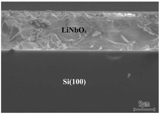
Figure 1.
Cross-section view of the LiNbO3/Si layered structure.
To investigate the crystal structure perfection of the bonded LiNbO3/Si layered structure, a double axis X-ray diffractometer was used on the KMC3 optical beamline at the BESSY II synchrotron radiation source. The X-ray diffraction method makes it possible to study the crystal structure perfection of both the LiNbO3 crystal and the Si crystal. The investigations were carried out at an X-ray energy of E = 8 keV (an X-ray wavelength of λ = 1.55 Å). The use of intense synchrotron radiation made it possible to measure the rocking curves of the layered structure for the LiNbO3 crystal layer and the underlying Si crystal layer. Figure 2 shows the measured rocking curves of the 41° YX-cut of a LiNbO3 crystal (a) and the Si(100) crystal (b). In the 41° YX-cut of a LiNbO3 crystal, planes (012) and (024) were parallel to the crystal surface. The rocking curve of the LiNbO3 crystal was measured for the reflection from the planes (024). The value of the Bragg angle was Θ(024) = 24.511°, and the full width at half maximum of the rocking curve was FWHM(024) = 0.006°. In the case of the Si crystal, the rocking curve was measured for reflection from the planes (400). In this case, the value of the Bragg angle was Θ(400) = 49.034°, and the full width at half maximum of the rocking curve was FWHM(400) = 0.010°. The calculated values of the full width at half maximum of the rocking curve were FWHM(024) = 0.0022° for the 41° YX-cut of a LiNbO3 crystal and FWHM(400) = 0.0011° for the Si(100) crystal. The difference between the experimental and calculated values of the full widths at half maximum of the rocking curves of the LiNbO3 and Si crystals indicates the distortion of the crystal lattices during bonding. In this case, the deformations occur at the LiNbO3/Si interface because the materials are bonded at high temperatures of ~600 °C. The materials have different coefficients of thermal expansion, which leads to the appearance of deformations in the crystal lattices during cooling.
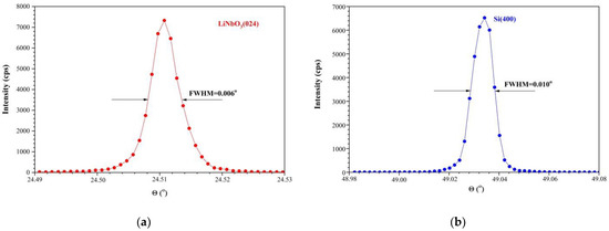
Figure 2.
Rocking curves of the LiNbO3/Si layered structure: (a) LiNbO3, reflection (024); (b) Si, reflection (400).
To study the SAW propagation in the LiNbO3/Si layered structure, the structures of the interdigital transducers (IDT) were fabricated on the LiNbO3 crystal surface by photolithography method to excite the SAW with a wavelength of Λ = 30 μm. The IDT consists of 26 pairs of aluminum electrodes, and the IDT aperture is equal to 60 SAW wavelengths (1.8 mm). The width and thickness of the Al-electrode is 7.5 µm and 100 nm, respectively. The velocities of the SAW and PSAW propagation in the 41° YX-cuts of a LiNbO3 crystal are VSAW = 3641 m/s and VPSAW = 4749 m/s, respectively [33]. The presence of a thin crystal LiNbO3 layer allows the excitation of the SAW with higher velocity in the LiNbO3/Si layered structure, which should propagate along the [110] direction. The SAW velocity in the Si(100) along direction [110] did not exceed 5080 m/s [34,35]. A number of papers [6,36] have demonstrated that the SAW and PSAW velocities in layered structures can exceed the velocities of their respective bulk crystals. In comparison, a similar IDT structure was also fabricated on the surface of a bulk 41° YX-cut of a LiNbO3 crystal.
Figure 3 shows the electrical characterization S11 of the LiNbO3/Si layered structure (red line) and the 41° YX-cut of a LiNbO3 crystal (blue line) under the SAW and PSAW excitation at a wavelength of Λ = 30 μm. The three resonances can be observed in the figure for the LiNbO3/Si layered structure. The first resonance is observable at a frequency of f = 135.4 MHz and corresponds to the SAW excitation in a thin crystal layer of the 41° YX-cut of a LiNbO3 crystal. In this case, the SAW propagation velocity is VSAW = f × Λ = 135.4 × 30 = 4062 m/s, which exceeds the value of the SAW velocity on the surface of the 41° YX-cut of thick LiNbO3 crystal (VSAW = 3641 m/s) [33]. The second resonance at the frequency of f = 157.7 MHz corresponds to the PSAW excitation in a thin crystal layer of the 41° YX-cut of a LiNbO3 crystal. This resonance is very intense because of the high value of the electromechanical coupling coefficient for the PSAW in the 41° YX-cut of a LiNbO3 crystal , while the electromechanical coupling coefficient for the SAW is only [33]. The PSAW propagation velocity is VPSAW = 157.7 × 30 = 4731 m/s, which corresponds to the value of the known PSAW velocity in the 41° YX-cut of a LiNbO3 crystal (VPSAW = 4749 m/s) [33]. The third resonance at f MHz corresponds to the SAW excitation in the LiNbO3/Si layered structure. In this case, the velocity of the SAW propagation is VSAW = 195.7 × 30 = 5871 m/s, which exceeds the value of the SAW and PSAW velocities in the Si(100) along the [110] direction (VSAW = 5080 m/s, VPSAW = 5570 m/s) [35,36,37,38].
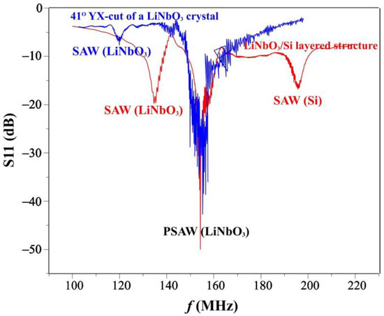
Figure 3.
Electrical characterization S11 of the LiNbO3/Si layered structure (red line) and 41° YX-cut of a LiNbO3 crystal (blue line).
Only two resonances can be observed for the 41° YX-cut of a LiNbO3 crystal on Figure 3. The first resonance at f = 123.1 MHz corresponds to the SAW with a velocity of VSAW = 3639 m/s, which correlates with the known velocity value for the 41° YX-cut of a LiNbO3 crystal [33]. The second resonance corresponds to the PSAW excitation at f = 157.7 MHz. Thus, the SAW velocity in the LiNbO3/Si layered structure is higher than that of the bulk 41° YX-cut of a LiNbO3 crystal, while the PSAW velocities coincide.
3. Scanning Electron Microscopy Set-Up for Investigation of SAW and PSAW Propagation
The scanning electron microscopy method allows one to visualize the surface, pseudo-surface, bulk, and the propagation of standing and traveling acoustic waves in the real-time mode [30,31,32,37,38]. SEM, when set to register the secondary electron emission from the crystal surface, allows us to visualize the distribution of the electric potential on the crystal surface, since the low-energy secondary electrons with an energy of 1 ÷ 3 eV are sensitive to the electric field that accompanies the propagation of acoustic waves in piezoelectric and ferroelectric crystals. To study the propagation process of the surface acoustic wave using the SEM method, it is necessary to use the accelerating voltage of E = 1 keV and an electron beam current of I = 1 nA. The use of a higher accelerating voltage is not possible, since, in this case, the piezoelectric substrate is strongly charged, which leads to the deflection of the primary electron beam and changes in the secondary electron emission from the crystal surface. Two methods can be used for visualization of the acoustic waves.
The first method is the stroboscopic scanning electron microscopy method, when the primary electron beam is modulated with the SAW frequency [39,40]. In this case, the electron beam is in a phase synchronization with the acoustic wave and remains in the same position at all times, since the secondary electron emission from the crystal surface is determined by the electric field that accompanies the SAW propagation in piezoelectric and ferroelectric crystals. This method requires a special upgrade to the scanning electron microscope (a stroboscopic system that deflects an electron beam with the frequency of an acoustic wave).
In the second method, which is more convenient (because it is not necessary to use the special stroboscopic technique), the high-frequency modulation of the low energy secondary electrons is defined by the electric field of the SAW (the minima and maxima of the SAW have different potentials and different coefficients of secondary electron emission from the crystal surface, respectively) and by the component, normal to the surface, of the electromagnetic radiation field of the IDT. The positive half-wave of the electromagnetic field accelerates the low-energy secondary electrons from the crystal surface to the secondary electron detector, while the negative half-wave prohibits the secondary electrons from reaching the detector. The electromagnetic and acoustic waves are mutually coherent, since they are excited by the same source (IDT) and with the same frequency. In this case, an image of the acoustic wave field on the crystal surface is observed only at the moment of the positive half-wave of the electromagnetic radiation field of the IDT and the SAW is observed always in the same position [31,32].
SEM methods make it possible to determine the acoustic wavelengths, to measure the power flow angles, to visualize the diffraction phenomena in acoustic beams, and to study the process of acoustic wave interaction with the crystal structure defects. The second method was used to visualize the SAW and PSAW propagation process in a bonded LiNbO3/Si layered structure.
4. SEM Imaging of the SAW and PSAW Propagation in a LiNbO3/Si Layered Structure
Figure 4 shows the SEM photomicrographs of the SAW and PSAW propagation in a bonded LiNbO3/Si layered structure. Microphotograph 4(a) displays an image of the traveling SAW with a wavelength of Λ = 30 μm, excited at the resonance frequency of f = 135.4 MHz. Both the IDT and acoustic wave field with a periodic SAW structure can be observed in the microphotograph. The dark lines of the SAW image correspond to the positive potential, which leads to a decrease in emission of the low-energy secondary electrons from the crystal surface. The bright lines, on the contrary, correspond to a negative potential and lead to an increase in the emission of the low-energy secondary electrons from the crystal surface. In this case, there is an even distribution of SAW. There are no diffraction phenomena in the acoustic beam; there is no distortion of the wave front. The SAW autocollimation can be observed. The SAW velocity in a bonded LiNbO3/Si layered structure is VSAW = 4062 m/s, which significantly exceeds the velocity of the bulk 41° YX-cut of a LiNbO3 crystal.
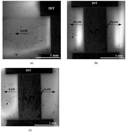
Figure 4.
SEM microphotographs of the SAW and PSAW in a LiNbO3/Si layered structure: (a) SAW, f = 135.4 MHz; (b) PSAW, f = 155.7 MHz; (c) SAW, f = 195.7 MHz. Λ = 30 µm.
Figure 4b shows a PSAW image with a wavelength of Λ = 30 μm in a LiNbO3/Si layered structure. The resonance excitation frequency of PSAW is f = 155.7 MHz, and the PSAW velocity is VPSAW = 4731 m/s. This PSAW velocity value is almost the same as the known PSAW velocity value VPSAW = 4749 m/s for the 41° YX-cut of a LiNbO3 crystal [33]. In this case, there is also no diffraction phenomena in the acoustic beam.
Figure 4c shows the microphotograph of the SAW with a wavelength of Λ = 30 μm, excited at the resonance frequency of f = 195.7 MHz and propagating with a velocity of VSAW = 5871 m/s in a LiNbO3/Si layered structure, which strongly exceeds the SAW velocity in the silicon crystal. The SAW image can be observed only in piezoelectric and ferroelectric crystals, where the SAW propagation causes a change in potential with a period corresponding to the SAW wavelength. In this case, the SAW propagates in a LiNbO3/Si layered structure. The SAW propagates in a LiNbO3/Si layered structure and causes a uniform sinusoidal deformation of a crystal lattice in the layer of the 41° YX-cut of a LiNbO3 crystal, which leads to a periodic distribution of the electric potential corresponding to the SAW period. Thus, it is possible to visualize the high-velocity traveling SAW in a LiNbO3/Si layered structure. In the figure on both sides of the IDT, the SAW wave field can be observed, in which there are no diffraction phenomena and no distortion of the SAW wave front.
The brighter contrast at Figure 4 corresponds to the highest value of the SAW amplitude. Usually, this is observable near the IDT. This effect can especially be observed at Figure 4b for the PSAW, because of the high value of the electromechanical coupling coefficient for the PSAW excitation in the 41° YX-cut of a LiNbO3 crystal. The PSAW flows deep into the crystal and at a small distance from the IDT the wave contrast is decreased.
Figure 5 presents the SEM microphotographs of the SAW (a) and PSAW (b) excitation in a bulk 41° YX-cut of a LiNbO3 crystal. The SAW with a wavelength of Λ = 30 µm was excited at f = 121.3 and propagates with a velocity of VSAW = 3639 m/s, while the PSAW was excited at f = 155.7 MHz and propagates with a velocity of VPSAW = 4731 m/s.
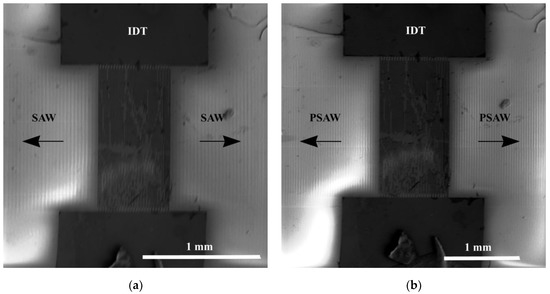
Figure 5.
SEM microphotographs of the SAW (a) and PSAW (b) in a bulk 41° YX-cut of a LiNbO3 crystal excited at f = 121.3 and f = 155.7 MHz, respectively. Λ = 30 µm.
In the case of the bulk 41° YX-cut of a LiNbO3 crystal there is also no diffraction phenomena in the acoustic beam and a uniform distribution of the amplitude along the wave front. However, it is very often possible to observe the diffraction phenomena in the acoustic beam. For example, in Figure 6 under the condition of acoustic beam autocollimation one can observe the strong Fresnel diffraction pattern in the acoustic beam. In this case, the SAW with a wavelength of Λ = 30 µm was excited in the YZ-cut of a LiNbO3 crystal by the IDT at a resonance excitation frequency of f = 116.27 MHz (VSAW ≈ 3488 m/s).
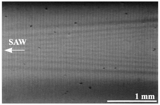
Figure 6.
SEM microphotograph of the traveling SAW propagation in the YZ-cut of a LiNbO3 crystal. f = 116.27 MHz, Λ = 30 µm.
5. Conclusions
The excitation and propagation processes of the SAW and PSAW in the bonded LiNbO3/Si layered structure and in the bulk 41° YX-cut of a LiNbO3 crystal were investigated using the scanning electron microscopy method. The layer thickness of the 41° YX-cut of a LiNbO3 crystal in the bonded LiNbO3/Si layered structure was 8 μm. The SEM method allowed for the visualization of the SAW and PSAW propagation in a LiNbO3/Si layered structure. The studies have shown that the SAW propagation in layered structures differs from the acoustic wave propagation in bulk crystals. Thus, the SAW propagation velocity in the bonded LiNbO3/Si layered structure was VSAW = 4062 m/s, which is significantly higher than that of the bulk substrate of the 41° YX-cut of a LiNbO3 crystal VSAW = 3642 m/s. At the same time, the PSAW propagation velocity is VPSAW = 4731 m/s and practically corresponds to the PSAW velocity in the bulk substrate of the 41° YX-cut of a LiNbO3 crystal (VPSAW = 4749 m/s) [33]. The scanning electron microscope also made it possible to observe the SAW at a velocity of VSAW = 5871 m/s in the bonded LiNbO3/Si layered structure, which exceeds the value of the SAW and PSAW velocities in the Si(100) along the [110] direction (VSAW = 5080 m/s, VPSAW = 5570 m/s).
It should be noted that the application of the SEM method allowed for not only the determination of the acoustic wave velocities, but also the visualization of the acoustic wave field in the bonded layered structure. It is necessary to note the absence of diffraction phenomena and divergence of the acoustic beam, and the absence of wave front distortion in the layered structure based on the 41° YX-cut of a LiNbO3 crystal and Si(100) crystal.
Thus, the scanning electron microscopy method made it possible to study the excitation and propagation of the SAW and PSAW in the bonded LiNbO3/Si layered structure and to observe the acoustic wave fields.
In the future, it is advisable to study the propagation of acoustic waves in such layered structures on synchrotron radiation sources by the X-ray diffraction and topography methods. X-ray methods will make it possible to study the propagation of traveling SAW both in the LiNbO3 crystal layer and in the Si crystal. Of particular interest is the study of the SAW propagation in the Si crystal at high velocity when, at one Bragg angle (the Bragg angle for reflection (400) in Si crystal), the process of SAW propagation in silicon crystal is investigated, and at another value of Bragg angle (the Bragg angle for reflection (012) or (024) in LiNbO3 crystal), the SAW propagation is studied in a thin layer of LiNbO3 crystal. Application of the X-ray diffraction method will allow for the comparison of the SAW amplitudes in the LiNbO3 and Si crystals. Unfortunately, due to the COVID-19 pandemic, it is unlikely that these experimental studies at a synchrotron radiation source can be realized in the near future.
Author Contributions
Conceptualization, D.R.; SAW device design, E.E.; fabrication of layered structure, A.M.; investigations, D.R., E.E., O.P., A.M., and O.T.; writing—original draft preparation, D.R. All authors have read and agreed to the published version of the manuscript.
Funding
This research is supported by Ministry of Science and Higher Education of the Russian Federation (grant number 075-15-2020-791).
Data Availability Statement
All relevant data presented in the article are stored according to institutional requirements and as such are not available online. However, all data used in this manu- script can be made available upon request to the authors.
Conflicts of Interest
The authors declare no conflict of interest.
References
- Dieulesaint, E.; Royer, D. Ondes Elastique Dans les Solids; Masson: Paris, France, 1974; pp. 5–339. [Google Scholar]
- Farnell, G. Properties of Elastic Surface Waves. In Physical Acoustics; Mason, W., Thurston, R., Eds.; Academic: New York, NY, USA, 1970; Volume 6, pp. 109–166. [Google Scholar]
- Campbell, C. Surface Acoustic Wave Devices for Mobile and Wireless Communications; Academic Press: Boston, MA, USA, 1998; pp. 1–631. [Google Scholar]
- Namba, A.; Sugimoto, M.; Ogura, T.; Tomita, Y.; Eda, K. Direct bonding of piezoelectric crystal onto silicon. Appl. Phys. Lett. 1995, 67, 3275–3276. [Google Scholar] [CrossRef]
- Takagi, H.; Maeda, R. Room-temperature bonding of lithium niobate and silicon wafers by argon-beam surface activation. Appl. Phys. Lett. 1999, 74, 2387–2389. [Google Scholar] [CrossRef]
- Jia, Y.; Wang, L.; Chen, F. Ion-cut lithium niobate on insulator technology: Recent advances and perspectives. Appl. Phys. Rev. 2021, 8, 011307. [Google Scholar] [CrossRef]
- Solal, M.; Pastureaud, T.; Ballandras, S.; Aspar, B.; Biasse, B.; Daniau, W.; Steichen, W.; Laude, V.; Laëns, A. Oriented lithium niobate layers transferred on 4" (100) silicon wafer for RF SAW devices. In IEEE Ultrasonic Symposium, Proceedings of the IEEE 2002, Munich, Germany, 8–11 October 2002; IEEE: Piscataway Township, NJ, USA, 2002; pp. 128–131. [Google Scholar]
- Pastureaud, T.; Solal, M.; Biasse, B.; Aspar, B.; Briot, J.-B.; Daniau, W.; Steichen, W.; Lardat, R.; Laude, V.; Laëns, A.; et al. High-Frequency Surface Acoustic Waves Excited on Thin-Oriented LiNbO3 Single-Crystal Layers Transferred Onto Silicon. IEEE Trans. Ultrason. Ferroelectr. Freq. Control 2007, 54, 870–876. [Google Scholar] [CrossRef] [PubMed]
- Tian, X.-G.; Liu, H.; Tao, L.-Q.; Yang, Y.; Jiang, H.; Ren, T.-L. High-resolution, high-linearity temperature sensor using surface acoustic wave device based on LiNbO3/SiO2/Si substrate. AIP Adv. 2016, 6, 095317. [Google Scholar] [CrossRef] [Green Version]
- Rabiei, P.; Ma, J.; Khan, S.; Chiles, J.; Fathpour, S. Heterogeneous lithium niobate photonics on silicon substrates. Opt. Express 2013, 21, 25573–25581. [Google Scholar] [CrossRef] [PubMed]
- Chen, L.; Wood, M.G.; Reano, R.M. 12.5 pm/V hybrid silicon and lithium niobate optical microring resonator with integrated electrodes. Opt. Express 2013, 21, 27001–27010. [Google Scholar] [CrossRef] [PubMed]
- Lee, Y.S.; Kim, G.-D.; Kim, W.-J.; Lee, S.-S.; Lee, W.-G.; Steier, W.H. Hybrid Si-LiNbO3Si-LiNbO3 microring electro-optically tunable resonators for active photonic devices. Opt. Lett. 2011, 36, 1119–1121. [Google Scholar]
- Chen, L.; Reano, R.M. Compact electric field sensors based on indirect bonding of lithium niobate to silicon microrings. Opt. Expres 2012, 20, 4032–4038. [Google Scholar] [CrossRef]
- Janner, D.; Tulli, D.; Jofre, M.; Yudistira, D.; Balsamo, S.; Belmonte, M.; Pruneri, V. Domain Inverted Acousto- and Electrooptic Devices and Their Application to Optical Communications, Sensing, Laser Sources, and Quantum Key Distribution. IEEE J. Sel. Top. Quantum Eletron. 2013, 19, 3400610. [Google Scholar] [CrossRef]
- Lilienblum, M.; Soergel, E. Anomalous domain inversion in LiNbO3 single crystals investigated by scanning probe microscopy. J. Appl. Phys. 2011, 110, 052018. [Google Scholar] [CrossRef] [Green Version]
- Lilienblum, M.; Ofan, A.; Hoffmann, Á.; Gaathon, O.; Vanamurthy, L.; Bakhru, S.; Bakhru, H.; Osgood, R.M.; Soergel, E. Low-voltage nanodomain writing in He-implanted lithium niobate crystals. Appl. Phys. Lett. 2010, 96, 082902. [Google Scholar] [CrossRef] [Green Version]
- Terabe, K.; Nakamura, M.; Takekawa, S.; Kitamura, K.; Higuchi, S.; Gotoh, Y.; Cho, Y. Microscale to nanoscale ferroelectric domain and surface engineering of a near-stoichiometric LiNbO3 crystal. Appl. Phys. Lett. 2003, 82, 433. [Google Scholar] [CrossRef]
- Vianne, B.; Richard, M.-I.; Escoubas, S.; Labat, S.; Schulli, T.; Chahine, G.; Fiori, V.; Thomas, O. Through-silicon via-induced strain distribution in silicon interposer. Appl. Phys. Lett. 2015, 106, 141905. [Google Scholar] [CrossRef]
- Zhao, P.; Likforman, J.P.; Li, H.Y.; Tao, J.; Henner, T.; Lim, Y.D.; Seit, W.W.; Tan, C.S.; Guidoni, L. TSV-integrated surface electrode ion trap for scalable quantum information processing. Appl. Phys. Lett. 2021, 118, 124003. [Google Scholar] [CrossRef]
- Sauer, W.; Streibl, M.; Metzger, T.H.; Haubrich, A.G.C.; Manus, S.; Wixforth, A.; Peisl, J.; Mazuelas, A.; Härtwig, J.; Baruchel, J. X-ray imaging and diffraction from surface phonons on GaAs. Appl. Phys. Lett. 1999, 75, 1709–1711. [Google Scholar] [CrossRef]
- Roshchupkin, D.; Ortega, L.; Plotitcyna, O.; Irzhak, D.; Emelin, E.; Fahrtdinov, R.; Alenkov, V.; Buzanov, O. Piezoelectric La3Ga5.3Ta0.5Al0.2O14 crystal: Growth, crystal structure perfection, piezoelectric, and acoustic properties. Appl. Phys. A 2014, 116, 1477–1488. [Google Scholar] [CrossRef]
- Roshchupkin, D.; Ortega, L.; Plotitcyna, O.; Zizak, I.; Vadilonga, S.; Irzhak, D.; Emelin, E. X-ray diffraction by surface acoustic waves. J. Appl. Crystallogr. 2021, 54, 180–194. [Google Scholar] [CrossRef]
- Tucoulou, R.; Pascal, R.; Brunel, M.; Mathon, O.; Roshchupkin, D.V.; Schelokov, I.A.; Cattan, E.; Remiens, D. X-ray diffraction from perfect silicon crystals distorted by surface acoustic waves. J. Appl. Crystallogr. 2000, 33, 1019–1022. [Google Scholar] [CrossRef] [Green Version]
- Tucoulou, R.; de Bergevin, F.; Mathon, O.; Roshchupkin, D. X-ray Bragg diffraction of LiNbO3 crystals excited by surface acoustic waves. Phys. Rev. B 2001, 64, 134108. [Google Scholar] [CrossRef]
- Whatmore, R.W.; Goddard, P.A.; Tanner, B.K.; Clark, G.F. Direct imaging of travelling Rayleigh waves by stroboscopic X-ray topography. Nature 1982, 299, 44–46. [Google Scholar] [CrossRef]
- Zolotoyabkoa, E.; Shilo, D.; Sauer, W.; Pernot, E.; Baruchel, J. Visualization of 10 µm surface acoustic waves by stroboscopic x-ray topography. Appl. Phys. Lett. 1998, 73, 2278–2280. [Google Scholar] [CrossRef]
- Roshchupkin, D.V.; Roshchupkina, H.D.; Irzhak, D.V. X-Ray Topography Analysis of Acoustic Wave Fields in the SAW-Resonator Structures. IEEE Trans. Ultrason. Ferroelectr. Freq. Control 2005, 52, 2081–2087. [Google Scholar] [CrossRef] [PubMed]
- Roshchupkin, D.; Ortega, L.; Snigirev, A.; Snigireva, I. X-ray imaging of the surface acoustic wave propagation in La3Ga5SiO14 crystal. Appl. Phys. Lett. 2013, 103, 154101. [Google Scholar] [CrossRef]
- Roshchupkin, D.; Ortega, L.; Zizak, I.; Plotitcyna, O.; Matveev, V.; Kononenko, O.; Emelin, E.; Erko, A.; Tynyshtykbayev, K.; Irzhak, D.; et al. Surface acoustic wave propagation in graphene film. J. Appl. Phys. 2015, 118, 104901. [Google Scholar] [CrossRef]
- Eberharter, G.; Feuerbaum, H.P. Scanning-elctron-microscope observations of propagating acoustic waves in surface acoustic wave devices. Appl. Phys. Lett. 1980, 37, 698. [Google Scholar] [CrossRef]
- Roshchupkin, D.V.; Brunel, M. Scanning electron microscopy observation of surface acoustic wave propagation in the LiNbO3 crystals with regular domain structures. IEEE Trans. Ultrason. Ferroelectr. Freq. Control 1994, 41, 512–517. [Google Scholar] [CrossRef]
- Roshchupkin, D.V.; Brunel, M.; Tucoulou, R.; Bigler, E.; Sorokin, N.G. Reflection of surface acoustic waves on domain walls in a LiNbO3 crystal. Appl. Phys. Lett. 1994, 64, 164–165. [Google Scholar] [CrossRef]
- Qiao, D.; Liu, W.; Smith, P.M. General Green’s Functions for SAW Devices Analysis. IEEE Trans. Ultrason. Ferroelectr. Freq. Control 1999, 46, 1242–1253. [Google Scholar] [CrossRef] [PubMed]
- Crean, G.M.; Waintal, A. Average Rayleigh-wave velocity of a computer-simulated crystallographic plane. J. Appl. Crystallogr. 1986, 19, 181–187. [Google Scholar] [CrossRef]
- Tarasenko, A.; Čtvrtlík, R.; Kudělka, R. Theoretical and experimental revision of surface acoustic waves on the (100) plane of silicon. Sci. Rep. 2021, 11, 2845. [Google Scholar] [CrossRef] [PubMed]
- Gomi, M.; Kataoka, T.; Hayashi, J.; Kakio, S. High-coupling leaky surface acoustic waves on LiNbO3 or LiTaO3 thin plate bonded to high-velocity substrate. Jpn. J. Appl. Phys. 2017, 56, 07JD13. [Google Scholar] [CrossRef]
- Caliendo, C. Theoretical Analysis of SAW Propagation in 3C-SiC/c-AlN. Crystals 2016, 6, 25. [Google Scholar] [CrossRef] [Green Version]
- Lin, C.-M.; Chen, Y.-Y.; Felmetsger, V.V.; Lien, W.-C.; Riekkinen, T.; Senesky, D.G.; Pisano, A.P. Surface acoustic wave devices on AlN/3C–SiC/Si multilayer structures. J. Micromech. Microeng. 2013, 23, 025019. [Google Scholar] [CrossRef]
- Bahadur, H.; Parshad, R. Scanning electron microscopy of vibrating quartz crystals. Scanning Electron. Microsc. 1980, 1, 509–522. [Google Scholar] [CrossRef]
- Feuerbaum, H.P.; Eberharter, G.; Tobolka, G. Visualization of traveling surface acoustic waves using a scanning electron microscope. Scanning Electron. Microsc. 1980, 1, 502–509. [Google Scholar]
Publisher’s Note: MDPI stays neutral with regard to jurisdictional claims in published maps and institutional affiliations. |
© 2021 by the authors. Licensee MDPI, Basel, Switzerland. This article is an open access article distributed under the terms and conditions of the Creative Commons Attribution (CC BY) license (https://creativecommons.org/licenses/by/4.0/).