Abstract
The electronic structure and band offsets of blue phosphorus/WSe2 van der Waals (vdW) heterostructure are investigated via performing first-principles calculations. Blue phosphorus/WSe2 vdW heterostructure exhibits modulation of bandgaps by the applied vertical compressive strain, and a large compressive strain of more than 23% leads to a semiconductor-to-metal transition. Blue phosphorus/WSe2 vdW heterostructure is demonstrated to have a type-II band alignment, which promotes the spontaneous spatial separation of photo-excited electrons and holes. Furthermore, electrons concentrating in BlueP and holes in WSe2 can be enhanced by applied compressive strain, resulting in an increase of carrier concentration. Therefore, these properties make blue phosphorus/WSe2 vdW heterostructure a good candidate for future applications in photodetection.
1. Introduction
Layered two-dimensional (2D) transition metal dichalcogenides (TMDs) and TMD-based vdW heterostructures have drawn tremendous attention and shown broad application prospects in next-generation electronic and optoelectronic devices because of their tunable electronic, optical, spintronic, and transport properties [1,2,3,4,5,6]. In recent years, 2D black phosphorus has received considerable attention for its unique properties including thickness-tunable direct band gap, high hole mobility, and other particular physical properties [7,8,9,10,11,12,13,14]. Meanwhile, blue phosphorus (BlueP), an allotrope of black phosphorus, has been successfully fabricated by mechanical exfoliation from its bulk form and even epitaxial growth methods [15,16,17,18,19]. The novel properties of BlueP and its vdW heterostructures have also been widely studied [20,21,22,23,24]. Li et al. designed a BlueP/borophene heterostructure and explored its performance as an anode material in lithium-ion batteries via first-principles calculations [25]. They found that the BlueP/borophene heterostructure possessed excellent structural stability and a specific capacity of 1019 mAh/g. Luo et al. theoretically predicted the hydrogen storage properties of Li-decorated single-layer BlueP from the view of its electronic and crystal structures [26]. It is demonstrated that hydrogen storage capacity was further improved by Li decoration due to enhanced adsorption of H to the Li atoms. Due to the promising performance of 2D vdW heterostructures [27,28,29,30,31], strain-induced properties of BlueP/GaN [32], BlueP/C3N [33], BlueP/Mg(OH)2 [34], and BlueP/black phosphorus [35] vdW heterostructures have been studied. However, strain-tunable electronic and optoelectronic properties of BlueP/TMDs vdW heterostructures have not been well-explored. It is of importance to explore the strain effect on the properties of BlueP/TMDs vdW heterostructures.
Therefore, in this work, a BlueP/WSe2 vdW heterostructure is constructed. The electronic structure and band offsets are investigated via utilizing first-principles calculations. It is illustrated that BlueP/WSe2 vdW heterostructure exhibits modulation of bandgaps by applying vertical compressive strain, which is accompanied by a semiconductor-to-metal transition under a large compressive strain more than 23%. A type-II band alignment of BlueP/WSe2 vdW heterostructure is demonstrated, since the band positions of BlueP and WSe2 straddle each other. In other words, the CBM and the VBM are contributed by BlueP and WSe2, respectively. Compared with other types of band alignments, the type-II band alignment is beneficial to the spatial separation of excited electrons and holes. Furthermore, the compressive strain can facilitate electrons in BlueP and holes in WSe2, resulting in an increase of carrier concentration.
2. Computational Model and Methods
The first-principles calculations are performed by using the projector-augmented plane-wave (PAW) method with the framework of density functional theory (DFT) in the VASP code. The GGA of PBE is adopted to describe the electron exchange and correlation. The pairwise force field in DFT-D2 method is used to describe the vdW interlayer interactions. The vacuum layer, the cutoff energy, the force tolerance, and the first Brillouin zone are 12 Å, 500 eV, 0.01 eV/Å and (9 × 9 × 1) Monkhorst–Pack grid. Figure 1a,b shows the top and side views of the 4 × 4 supercell structure of BlueP/WSe2 vdW heterostructure. The optimized lattice constants of BlueP and WSe2 are 3.28 and 3.29 Å [33,36], respectively, which indicates a very good lattice matching in this system. The effect of applied vertical strain on the electronic and optical properties of BlueP/WSe2 vdW heterostructure is study. The strain is calculated as ε = (d − d0)/d0, where d and d0 are the instantaneous and equilibrium distances between the bottom phosphorus atom layer and the tungsten atom layer, as shown in Figure 1b. So, a negative ε represents compressive strain and a positive one represents tensile strain. Figure 1c exhibits the Brillouin zone of hexagonal cell with high-symmetry points (M, K, and Γ) labeled, and the point between M and Γ is defined as Λ.
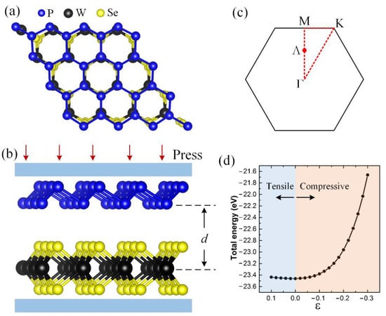
Figure 1.
(a) The top and (b) the side view of BlueP/WSe2 vdW heterostructure. (c) The Brillouin zone with high-symmetry points (M, K, and Γ) and the point Λ (between M and Γ) labeled. (d) Evolution of the total energy of BlueP/WSe2 vdW heterostructure as a function of vertical strain.
3. Results and Discussion
To determine the stable structure of BlueP/WSe2 vdW heterostructure, a variation of the total energy with the applied vertical strains is calculated in Figure 1d. The curve indicates the minimum under zero strain, and the equilibrium distance is d0 = 4.79 Å. Figure 1d also illustrates that the total energy of BlueP/WSe2 vdW heterostructure is sensitively tuned by compressive strain rather than tensile strain.
Band structures of monolayer BlueP, monolayer WSe2, and BlueP/WSe2 vdW heterostructure are exhibited in Figure 2. To explore the optoelectronic properties of BlueP/WSe2 vdW heterostructure, its band alignment is also calculated in Figure 2b. In the projected band structure in Figure 2a, lines in blue and red dots are the electronic bands dominated by BlueP and WSe2, respectively. Our results show that monolayer BlueP has an indirect bandgap of 1.94 eV, and monolayer WSe2 shows a direct bandgap of 1.55 eV. After combination, the indirect band gap of BlueP/WSe2 vdW heterostructure is reduced to 1.11 eV, with the conduction band minimum (CBM) and the valence band maximum (VBM) localizing at the Λ and K points, respectively. More importantly, the CBM and the VBM are mainly contributed by BlueP and WSe2, respectively, which indicates that BlueP/WSe2 vdW heterostructure is type-II heterostructure. As a result, spontaneous spatial separation of the lowest energy electron-hole pairs will occur in the vdW heterostructure with electrons and holes concentrating in BlueP and WSe2, respectively, as shown in Figure 2b. Further insight can be obtained from the band decomposed charge density of CBM and VBM of the BlueP/WSe2 vdW heterostructure in Figure 2c. It can be seen that the wavefunctions of the CBM and the VBM are localized on BlueP and WSe2, respectively. These results are also supported by the projected density of states (DOS) of BlueP/WSe2 vdW heterostructure, as displayed in Figure 2d. According to our results, the spatially separated photoexcited electrons and holes can effectively improve the carrier concentrations and photocurrent in the vdW heterostructure and further improve the optoelectronic property of BlueP/WSe2 vdW heterostructure.
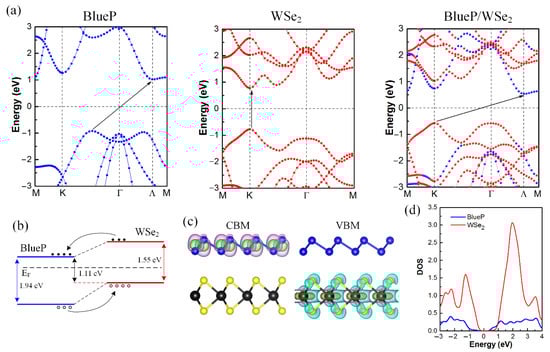
Figure 2.
(a) Band structures of monolayer BlueP, monolayer WSe2, and BlueP/WSe2 vdW heterostructure. (b) The band alignment, (c) the band decomposed charge density of CBM and VBM, and (d) the DOS of BlueP/WSe2 vdW heterostructure.
Projected band structures of BlueP/WSe2 vdW heterostructure under different vertical strains are illustrated in Figure 3. The bands contributed by BlueP and WSe2 are plotted by blue and red balls, respectively. The CBM is found to localize on the Λ and the VBM is found to localize on the K when BlueP/WSe2 vdW heterostructure is under a tensile strain of 0.08, as shown in Figure 3a. However, the VBM is changed from K to Γ when the strain is changed to a compressive strain of 0.08, but the CBM remains on Λ, as shown in Figure 3c. Interestingly, Figure 3d displays that the CBM is localized on both Λ and K, when continue increasing the compressive strain to 0.12. And after that, the CBM is changed to K, while the VBM remains on Γ, as displayed in Figure 3e. It is also proved that both the CBM and VBM move towards the Fermi level under applying vertical compressive strain, leading to a decreasing bandgap.
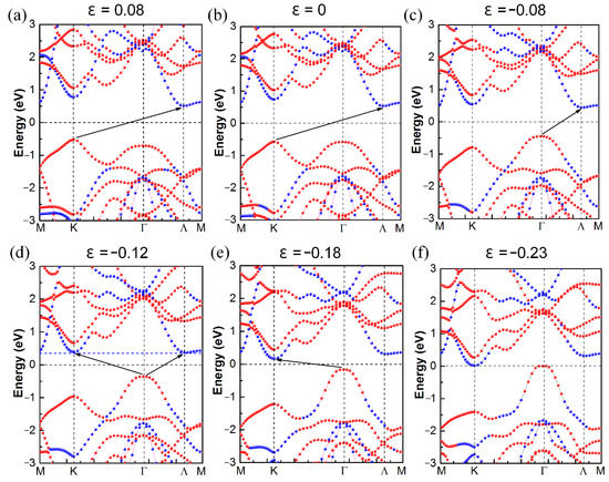
Figure 3.
(a–f) Projected band structures of BlueP/WSe2 vdW heterostructure under different vertical strain. The bands dominated by BlueP and WSe2 are plotted by blue and red balls, respectively.
The corresponding evolution of the bandgap of BlueP/WSe2 vdW heterostructure with the applied vertical strain is exhibited in Figure 4a. The bandgap reaches its maximum at the equilibrium state, and it decreases under tensile or compressive strain. Interestingly, compared with the tensile strain, the compressive strain shows much more remarkable tunability on the bandgap of BlueP/WSe2 heterostructure. Results in Figure 3 show that both the CBM and VBM move towards the Fermi level under applying vertical compressive strain, leading to a decreasing bandgap. When the compressive strain increases to more than 0.23, BlueP/WSe2 vdW heterostructure experiences a transition from semiconductor to metal, which can result in improved conductivity and enhanced transport properties.
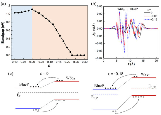
Figure 4.
(a) Evolution of the bandgap of BlueP/WSe2 vdW heterostructure as a function of the vertical strain. (b) The difference between the integrated charge density of BlueP/WSe2 vdW heterostructure under different compressive strain and that of isolated monolayers. (c) Band alignments of BlueP/WSe2 vdW heterostructure at the equilibrium state and under a compressive strain of 0.18, respectively.
The integrated charge density difference of BlueP/WSe2 vdW heterostructure under compressive strains is calculated in Figure 4b. The integrated charge density difference is calculated as:
where , , and are the charge density at the point of (x, y, z) in BlueP/WSe2, BlueP, and WSe2, respectively. It can be seen that the charge exchange at the interface of BlueP/WSe2 vdW heterostructure is weak at the equilibrium state. Then, more charge exchange appears with the increase of compressive strain. To quantify interlayer charge transfer in the vdW heterostructure, Bader charge analysis is employed to determine the resulted charge density of BlueP/WSe2 vdW heterostructure. The results indicated that the number of electrons transferred from WSe2 to BlueP is 0.0068, 0.008, and 0.0091 under the compressive strain of 0, 0.08, and 0.18, respectively. Therefore, it suggests that the compressive strain can facilitate electrons in BlueP and holes in WSe2, resulting in an increase of carrier concentration, as shown in Figure 4c.
Calculated optical properties of absorption coefficient and reflectivity of BlueP/WSe2 vdW heterostructure under different compressive strain are exhibited in Figure 5. The same optical properties are observed in x and y directions, due to the isotropy of the hexagonal lattice, as shown in Figure 5a,b. From the absorption spectrum, it can be found that BlueP/WSe2 vdW heterostructure would have excellent application in ultraviolet light (above 5 eV) detecting. Furthermore, Figure 5c indicates that the applied vertical compressive strain shows obvious influence on the optical properties in the z direction, while exerts little influence in x and y directions. The reason is that the applied vertical compressive strain only enhances the interlayer interaction while having a negligible effect on the in-plane interaction.
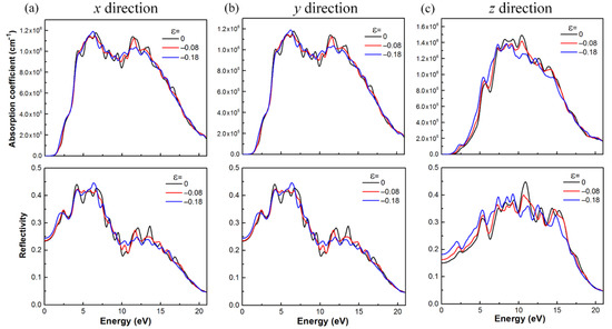
Figure 5.
Absorption coefficient and reflectivity in the (a) x direction, (b) y direction, and (c) z direction of BlueP/WSe2 vdW heterostructure under different compressive strains.
4. Conclusions
In summary, we have constructed a BlueP/WSe2 vdw heterostructure and investigated its electronic structure and band offsets via first-principles calculations. BlueP/WSe2 vdW heterostructure exhibits tunable bandgap by applied vertical compressive strain and even a semiconductor-to-metal transition is observed, which suggests a great application potential in future nano-electronics. Moreover, the type-II band alignment of BlueP/WSe2 vdW heterostructure facilitates the spatial separation of the photo-excited electron-hole pairs. The compressive strain facilitates electrons in BlueP and holes in WSe2, which results in an increase of carrier concentration. According to these results, BlueP/WSe2 vdW heterostructure presents a variety of opportunities for applications in future nano- and optoelectronic devices such as photodetectors and solar cells.
Author Contributions
Conceptualization, L.H. and Y.Y.; methodology, L.H. and Y.Y.; software, L.H. and Y.Y.; validation, L.Z. and T.Y.; formal analysis, L.Z. and T.Y.; investigation, L.H. and Y.Y.; resources, L.H. and Y.Y.; data curation, Y.Y.; writing—original draft preparation, Y.Y.; writing—review and editing, L.Z. and T.Y.; visualization, Y.Y.; supervision, L.Z. and T.Y.; project administration, L.Z. and T.Y.; funding acquisition, L.Z. All authors have read and agreed to the published version of the manuscript.
Funding
This research was funded by the Science Research Foundation of Education Department of Hunan Province (No. 17C1264).
Data Availability Statement
The data presented in this study are available within the article.
Conflicts of Interest
The authors declare no conflict of interest.
References
- Zhang, S.; Guo, S.; Chen, Z.; Wang, Y.; Gao, H.; Gomez-Herrero, J.; Ares, P.; Zamora, F.; Zhu, Z.; Zeng, H. Recent progress in 2D group-VA semiconductors: From theory to experiment. Chem. Soc. Rev. 2018, 47, 982–1021. [Google Scholar] [CrossRef] [PubMed]
- Long, M.; Wang, P.; Fang, H.; Hu, W. Progress, Challenges, and Opportunities for 2D Material Based Photodetectors. Adv. Funct. Mater. 2019, 29, 1803807. [Google Scholar] [CrossRef]
- Huo, N.; Konstantatos, G. Recent Progress and Future Prospects of 2D-Based Photodetectors. Adv. Mater. 2018, 30, 1801164. [Google Scholar] [CrossRef]
- Tan, C.; Zhang, H. Epitaxial growth of hetero-nanostructures based on ultrathin two-dimensional nanosheets. J. Am. Chem. Soc. 2015, 137, 12162–12174. [Google Scholar] [CrossRef]
- Bhimanapati, G.R.; Lin, Z.; Meunier, V.; Jung, Y.; Cha, J.; Das, S.; Xiao, D.; Son, Y.; Strano, M.S.; Cooper, V.R.; et al. Recent Advances in Two-Dimensional Materials beyond Graphene. ACS Nano 2015, 9, 11509–11539. [Google Scholar] [CrossRef]
- Baugher, B.W.H.; Churchill, H.O.H.; Yang, Y.; Jarillo-Herrero, P. Optoelectronic devices based on electrically tunable p-n diodes in a monolayer dichalcogenide. Nat. Nanotechnol. 2014, 9, 262–267. [Google Scholar] [CrossRef] [PubMed]
- Pang, J.B.; Bachmatiuk, A.; Yin, Y.; Trzebicka, B.; Zhao, L.; Fu, L.; Mendes, R.G.; Gemming, T.; Liu, Z.F.; Rummeli, M.H. Applications of Phosphorene and Black Phosphorus in Energy Conversion and Storage Devices. Adv. Energy Mater. 2018, 8, 43. [Google Scholar] [CrossRef]
- Hu, Z.H.; Niu, T.C.; Guo, R.; Zhang, J.L.; Lai, M.; He, J.; Wang, L.; Chen, W. Two-dimensional black phosphorus: Its fabrication, functionalization and applications. Nanoscale 2018, 10, 21575–21603. [Google Scholar] [CrossRef]
- Liu, H.; Hu, K.; Yan, D.; Chen, R.; Zou, Y.; Liu, H.; Wang, S. Recent Advances on Black Phosphorus for Energy Storage, Catalysis, and Sensor Applications. Adv. Mater. 2018, 30, 1800295. [Google Scholar] [CrossRef] [PubMed]
- Liu, S.; Huo, N.; Gan, S.; Li, Y.; Wei, Z.; Huang, B.; Liu, J.; Li, J.; Chen, H. Thickness-dependent Raman spectra, transport properties and infrared photoresponse of few-layer black phosphorus. J. Mater. Chem. C 2015, 3, 10974–10980. [Google Scholar] [CrossRef]
- Liu, H.; Neal, A.T.; Zhu, Z.; Luo, Z.; Xu, X.F.; Tomanek, D.; Ye, P.D. Phosphorene: An Unexplored 2D Semiconductor with a High Hole Mobility. ACS Nano 2014, 8, 4033–4041. [Google Scholar] [CrossRef]
- Guan, J.; Zhu, Z.; Tomanek, D. Phase coexistence and metal-insulator transition in few-layer phosphorene: A computational study. Phys. Rev. Lett. 2014, 113, 046804. [Google Scholar] [CrossRef]
- Su, Z.; Wang, Y. Anisotropic Photonics Topological Transition in Hyperbolic Metamaterials Based on Black Phosphorus. Nanomaterials 2020, 10, 1694. [Google Scholar] [CrossRef]
- Dai, X.; Qian, Z.; Lin, Q.; Chen, L.; Wang, R.; Sun, Y. Benchmark Investigation of Band-Gap Tunability of Monolayer Semiconductors under Hydrostatic Pressure with Focus-On Antimony. Nanomaterials 2020, 10, 2154. [Google Scholar] [CrossRef]
- Reich, E.S. Phosphorene excites materials scientists. Nature 2014, 506, 19. [Google Scholar] [CrossRef] [PubMed]
- Koenig, S.P.; Doganov, R.A.; Schmidt, H.; Castro Neto, A.H.; Özyilmaz, B. Electric field effect in ultrathin black phosphorus. Appl. Phys. Lett. 2014, 104, 103106. [Google Scholar] [CrossRef]
- Zhu, Z.; Tomanek, D. Semiconducting layered blue phosphorus: A computational study. Phys. Rev. Lett. 2014, 112, 176802. [Google Scholar] [CrossRef] [PubMed]
- Gu, C.D.; Zhao, S.T.; Zhang, J.L.; Sun, S.; Yuan, Z.D.; Hu, Z.H.; Han, C.; Ma, Z.R.; Wang, L.; Huo, F.W.; et al. Growth of Quasi-Free-Standing Single-Layer Blue Phosphorus on Tellurium Monolayer Functionalized Au(111). ACS Nano 2017, 11, 4943–4949. [Google Scholar] [CrossRef]
- Zhang, J.L.; Zhao, S.; Han, C.; Wang, Z.; Zhong, S.; Sun, S.; Guo, R.; Zhou, X.; Gu, C.D.; Yuan, K.D.; et al. Epitaxial Growth of Single Layer Blue Phosphorus: A New Phase of Two-Dimensional Phosphorus. Nano Lett. 2016, 16, 4903–4908. [Google Scholar] [CrossRef]
- Golias, E.; Krivenkov, M.; Varykhalov, A.; Sánchez-Barriga, J.; Rader, O. Band Renormalization of Blue Phosphorus on Au(111). Nano Lett. 2018, 18, 6672–6678. [Google Scholar] [CrossRef] [PubMed]
- Ahn, J.; Hong, I.; Kwon, Y.; Clay, R.C.; Shulenburger, L.; Shin, H.; Benali, A. Phase stability and interlayer interaction of blue phosphorene. Phys. Rev. B 2018, 98, 085429. [Google Scholar] [CrossRef]
- Zeng, J.; Cui, P.; Zhang, Z.Y. Half Layer By Half Layer Growth of a Blue Phosphorene Monolayer on a GaN(001) Substrate. Phys. Rev. Lett. 2017, 118, 5. [Google Scholar] [CrossRef]
- Ghosh, B.; Nahas, S.; Bhowmick, S.; Agarwal, A. Electric field induced gap modification in ultrathin blue phosphorus. Phys. Rev. B 2015, 91, 115433. [Google Scholar] [CrossRef]
- Zhang, J.L.; Han, C.; Hu, Z.; Wang, L.; Liu, L.; Wee, A.T.S.; Chen, W. 2D Phosphorene: Epitaxial Growth and Interface Engineering for Electronic Devices. Adv. Mater. 2018, 30, 1802207. [Google Scholar] [CrossRef] [PubMed]
- Li, Q.; Yang, J.; Zhang, L. Theoretical Prediction of Blue Phosphorene/Borophene Heterostructure as a Promising Anode Material for Lithium-Ion Batteries. J. Phys. Chem. C 2018, 122, 18294–18303. [Google Scholar] [CrossRef]
- Luo, D.; Li, J.; Zhang, Y.; Song, Y.; Chen, H. Electronic structure and hydrogen storage properties of Li–decorated single layer blue phosphorus. Int. J. Hydrogen Energy 2018, 43, 8415–8425. [Google Scholar] [CrossRef]
- Jariwala, D.; Marks, T.J.; Hersam, M.C. Mixed-dimensional van der Waals heterostructures. Nat. Mater. 2017, 16, 170–181. [Google Scholar] [CrossRef] [PubMed]
- Liu, Y.; Weiss, N.O.; Duan, X.; Cheng, H.-C.; Huang, Y.; Duan, X. Van der Waals heterostructures and devices. Nat. Rev. Mater. 2016, 16042. [Google Scholar] [CrossRef]
- Geim, A.K.; Grigorieva, I.V. Van der Waals heterostructures. Nature 2013, 499, 419–425. [Google Scholar] [CrossRef]
- Huang, L.; Li, Y.; Wei, Z.; Li, J. Strain induced piezoelectric effect in black phosphorus and MoS2 van der Waals heterostructure. Sci. Rep. 2015, 5, 16448. [Google Scholar] [CrossRef]
- Huang, L.; Li, J. Tunable electronic structure of black phosphorus/blue phosphorus van der Waals p-n heterostructure. Appl. Phys. Lett. 2016, 108, 083101. [Google Scholar] [CrossRef]
- Ren, K.; Wang, S.; Luo, Y.; Xu, Y.; Sun, M.; Yu, J.; Tang, W. Strain-enhanced properties of van der Waals heterostructure based on blue phosphorus and g-GaN as a visible-light-driven photocatalyst for water splitting. RSC Adv. 2019, 9, 4816–4823. [Google Scholar] [CrossRef]
- Gao, X.; Shen, Y.; Ma, Y.; Wu, S.; Zhou, Z. First-principles insights into efficient band gap engineering of the blue phosphorus/g-C3N bilayer heterostructure via an external vertical strain. Appl. Surf. Sci. 2019, 479, 1098–1104. [Google Scholar] [CrossRef]
- Wang, B.-J.; Li, X.-H.; Cai, X.-L.; Yu, W.-Y.; Zhang, L.-W.; Zhao, R.-Q.; Ke, S.-H. Blue Phosphorus/Mg(OH)2 van der Waals Heterostructures as Promising Visible-Light Photocatalysts for Water Splitting. J. Phys. Chem. C 2018, 122, 7075–7080. [Google Scholar] [CrossRef]
- Li, J.; Duan, H.; Zeng, B.; Jing, Q.; Cao, B.; Chen, F.; Long, M. Strain-Induced Band Structure Modulation in Hexagonal Boron Phosphide/Blue Phosphorene vdW Heterostructure. J. Phys. Chem. C 2018, 122, 26120–26129. [Google Scholar] [CrossRef]
- Kang, J.; Tongay, S.; Zhou, J.; Li, J.; Wu, J. Band offsets and heterostructures of two-dimensional semiconductors. Appl. Phys. Lett. 2013, 102, 012111. [Google Scholar] [CrossRef]
Publisher’s Note: MDPI stays neutral with regard to jurisdictional claims in published maps and institutional affiliations. |
© 2021 by the authors. Licensee MDPI, Basel, Switzerland. This article is an open access article distributed under the terms and conditions of the Creative Commons Attribution (CC BY) license (https://creativecommons.org/licenses/by/4.0/).