Abstract
Porous silicon (PSi) layers were formed on a p-type Si wafer. Six samples were anodised electrically with a 30 mA/cm2 fixed current density for different etching times. The samples were coated with a 50–60 nm gold layer and annealed at different temperatures under Ar flow. The morphology of the layers, before and after annealing, formed by this method was investigated by scanning electron microscopy (SEM). Photoacoustic spectroscopy (PAS) measurements were carried out to measure the thermal diffusivity (TD) of the PSi and Au/PSi samples. For the Au/PSi samples, the thermal diffusivity was measured before and after annealing to study the effect of annealing. Also to study the aging effect, a comparison was made between freshly annealed samples and samples 30 days after annealing.
1. Introduction
For several years diffusing with a gold layer has been used to control the electrical properties of silicon (Si) based devices, with several reports published on the study of gold diffusion into a silicon lattice [1,2]. Gold is highly reactive and miscible in Si, though a stable Au/Si compound does not exist, but rather a mixture of metastable [3,4] phases produced by thermal reaction and which is thought to exist under non-equilibrium conditions or in intermediate stages. The structure of metastable gold silicide is very complicated, consequently leading to various interpretations of the diffraction spectra. Investigations on gold silicide formation in thin films and the formation of metastable phases have been extensively carried out by several groups [5,6,7].
PSi is a strong light emitting material showing significant luminescence over a wide spectral range. Hence, a large amount of research work has focused on realizing porous silicon (PSi) based optoelectronic devices, such as light emitting diodes (LED) [8], waveguides [9], optical filters [8], thermal isolators [10], photovoltaic diodes [11], and different types of sensors [12]. The Au/PSi structure can be used as a hydrogen fuel cell or for other applications that require tuneable and lower thermal diffusivity than silicon. Photoluminescence [13], electrical [14,15], optical [16] and other properties of gold coated porous silicon (Au/PSi) have been reported to date; however, no reports on the thermal properties currently exist.
Here, we report a study on the structural and thermal properties of Au/PSi with different porosities annealed at different temperatures, including an investigation on the aging effect of all samples after 30 days. The samples were grouped in four sets and each set was made porous with six different etching times. The current density was fixed for all samples at 30 mA/cm2. Then an Au layer (50–60 nm) was coated on all samples at room temperature. The eutectic temperature of the Au-Si system is known as 365 °C from the phase diagram [17], so the above mentioned sets were annealed from 300 to 800 °C for one hour under Ar flow to cover the temperature range below and above the eutectic temperature. So the difference between sets can be considered as the annealing temperatures. As photoacoustic spectroscopy (PAS) is an accurate and non-destructive method, we chose it to measure the TD.
2. Results and Discussion
Sample thickness and porosity were calculated by the gravimetric method [18]. The samples were weighed before anodization (m1), immediately after anodization (m2), and after dissolution of the porous silicon layer in 1 M, NaOH aqueous solution (m3). The porosity and thickness respectively are given by the following equations:
where is the Si density and S is the anodised surface. The thickness of the PSi layers was also rechecked by Ambios Technology, a stylus profilometer, XP-200.
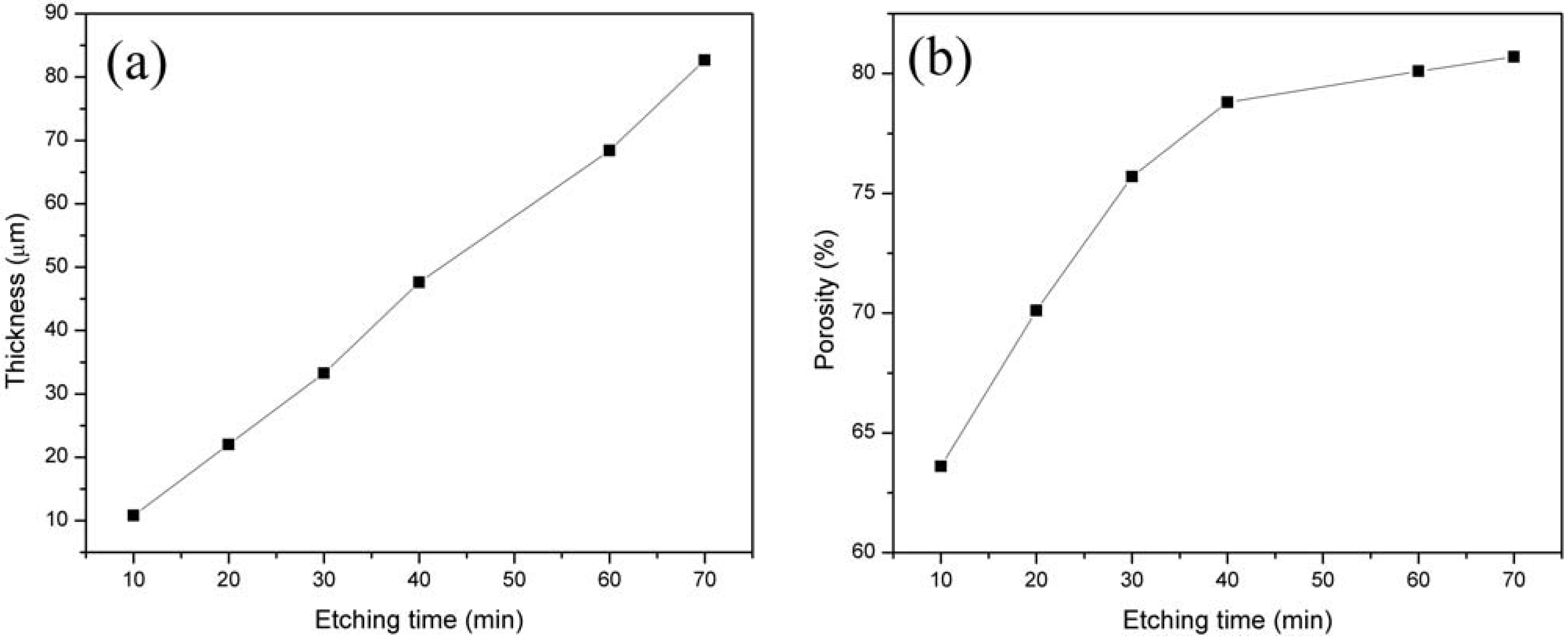
By using Equations 1 and 2 after measuring the mass of the samples, the density of substrate (ρ) and the anodized area (S), the porosity percentage and the thickness of the layer were calculated. The variation in porosity and thickness are shown in Figure 1. The thickness of the layers rises with increasing etch time. The average thickness of the PSi layers grows roughly linearly with etching time. The thickness of these samples was also measured with the stylus profilometer. The results are in a good agreement with the values in Figure 1(a). Notably, the porosity initially increases rapidly and levels off at approximately 79%.
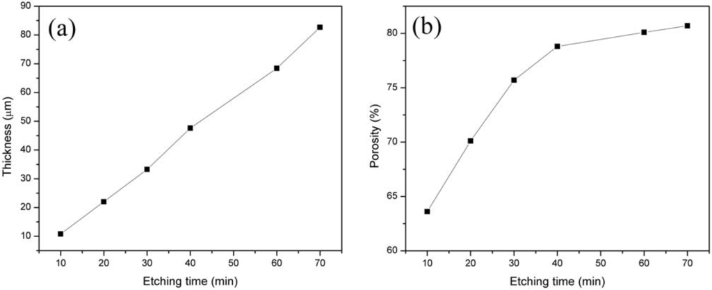
Figure 1.
(a) Thickness as a function of etching time; (b) Porosity as a function of etching time.
Figure 1.
(a) Thickness as a function of etching time; (b) Porosity as a function of etching time.
For structural characterization, the PSi layers were examined with scanning electron microscopy (SEM) before and after gold deposition. These images were carried out using a Hitachi, SN3400. SEM images show the PSi layer prepared on a Si substrate. The silicon structures were seen clearly on the top view in Figure 2(a), and cross sectional view in Figure 2(b). The top view shows that the size of the silicon structures are between 30–40 µm and the cross sectional view shows that the thickness of the layer for this sample is roughly around 20 µm.
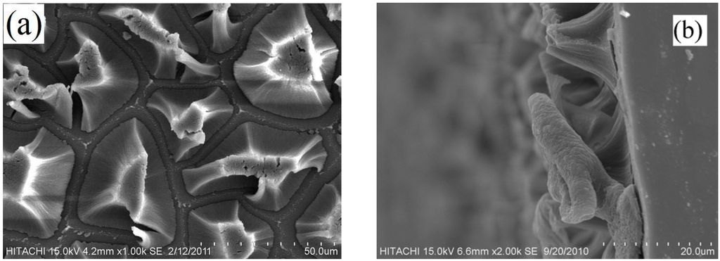
Figure 2.
(a) SEM image of a PSi layer; (b) Cross sectional view of a PSi layer.
Figure 2.
(a) SEM image of a PSi layer; (b) Cross sectional view of a PSi layer.
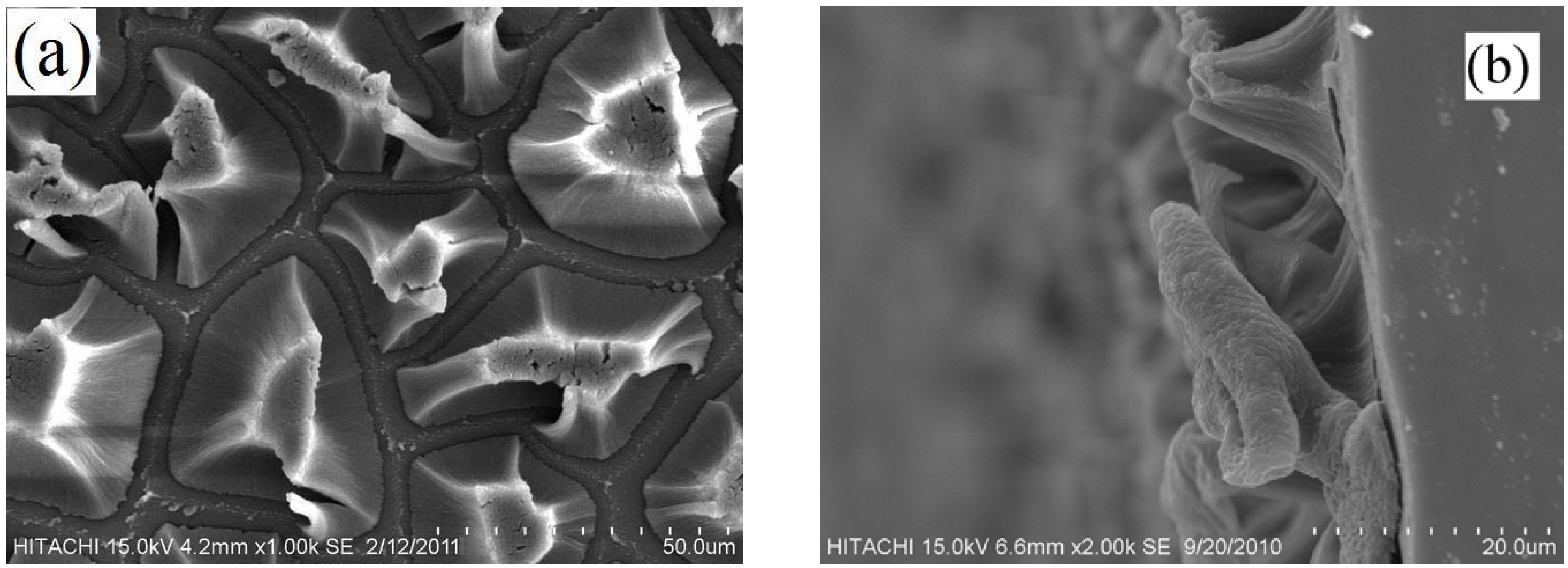
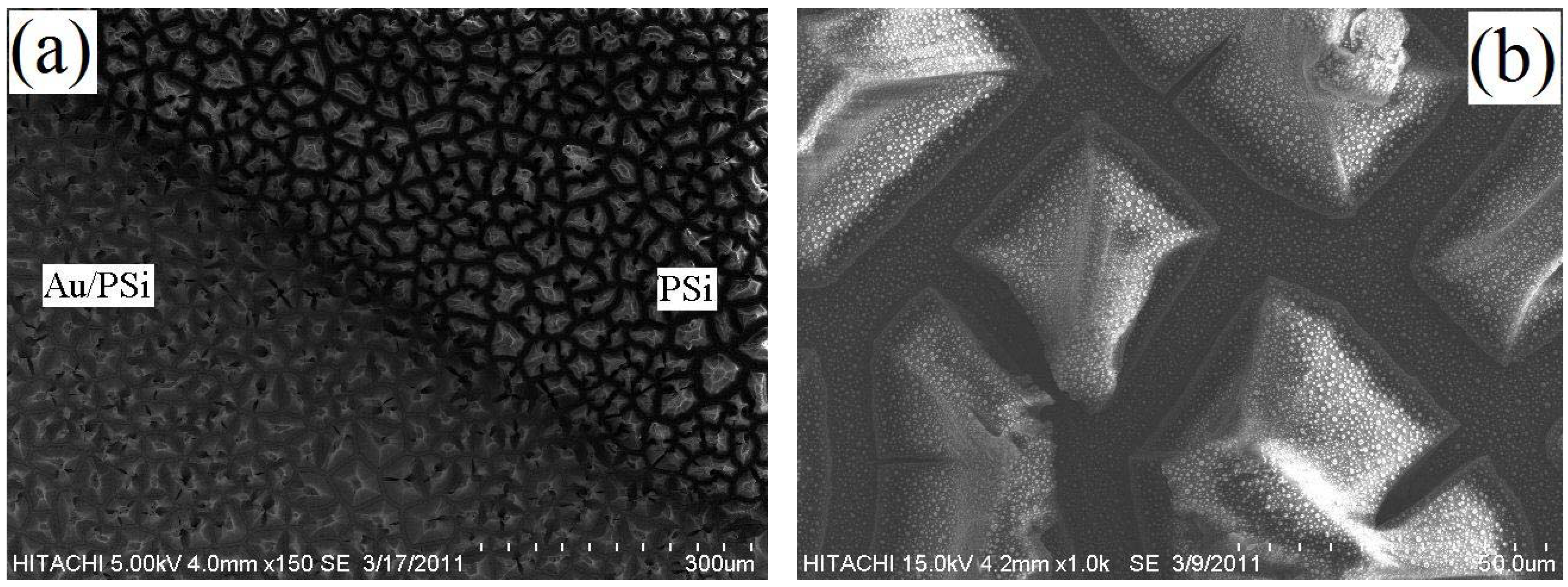
Figure 3(a) shows a PSi sample with half of the surface uniformly deposited with an Au thin film. According to Figure 3(b), a uniform dispersion of island-like Au particles, see white dots as shown by arrow, agglomerate with a SiOx matrix. This forms because of the low kinetic energy gained by sputtered Au atoms at room temperature, which lead to a slow diffusion rate and mobility [19,20].
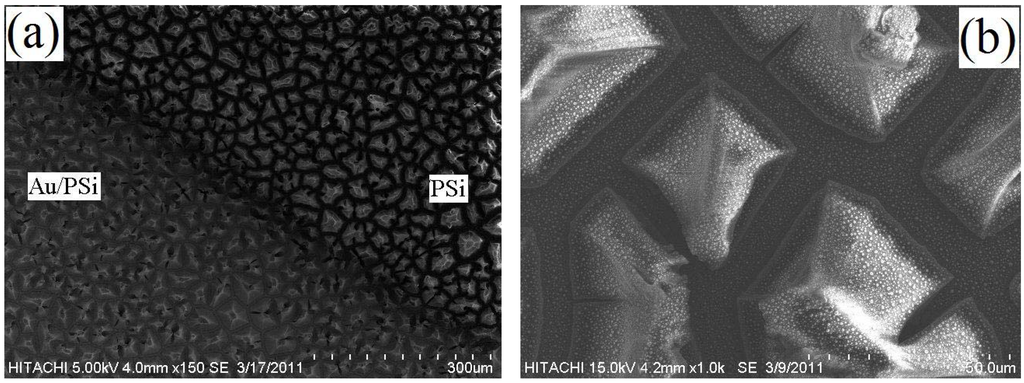
Figure 3.
(a) SEM image of a PSi sample with Au deposition on a part of the surface; (b) image of Au deposited PSi layer after annealing.
Figure 3.
(a) SEM image of a PSi sample with Au deposition on a part of the surface; (b) image of Au deposited PSi layer after annealing.
To describe the results of the PAS measurements we refer to the thermal piston in terms of the RG theory, developed by Rosencwaig and Gersho [21]. They believed the source of the acoustic signal in the cell is caused by the periodic heat flow of the solid to the ambient gas as the solid is heated by the modulated monochromatic beam. The pressure fluctuations are described as:
where γ is the air specific heat ratio, Po the ambient pressure, I0 the incident light beam intensity, f the chopping frequency; and li, ki, and αi, are the thickness, thermal conductivity and TD of material i, respectively. The subscript i can be both s and g, representing the sample and gas, respectively. TD (αi) is the rate of propagation of a temperature pulse in a material between two points. Thermal diffusivity defines as , where αi is TD, k is thermal conductivity, ρ is density, and Cv is the specific heat of the sample. The complex thermal diffusion coefficient of material i is defined as [21]:
where μi is the thermal diffusion length. Particularly, for a thermally thick sample (), PA amplitude (S) varies as:
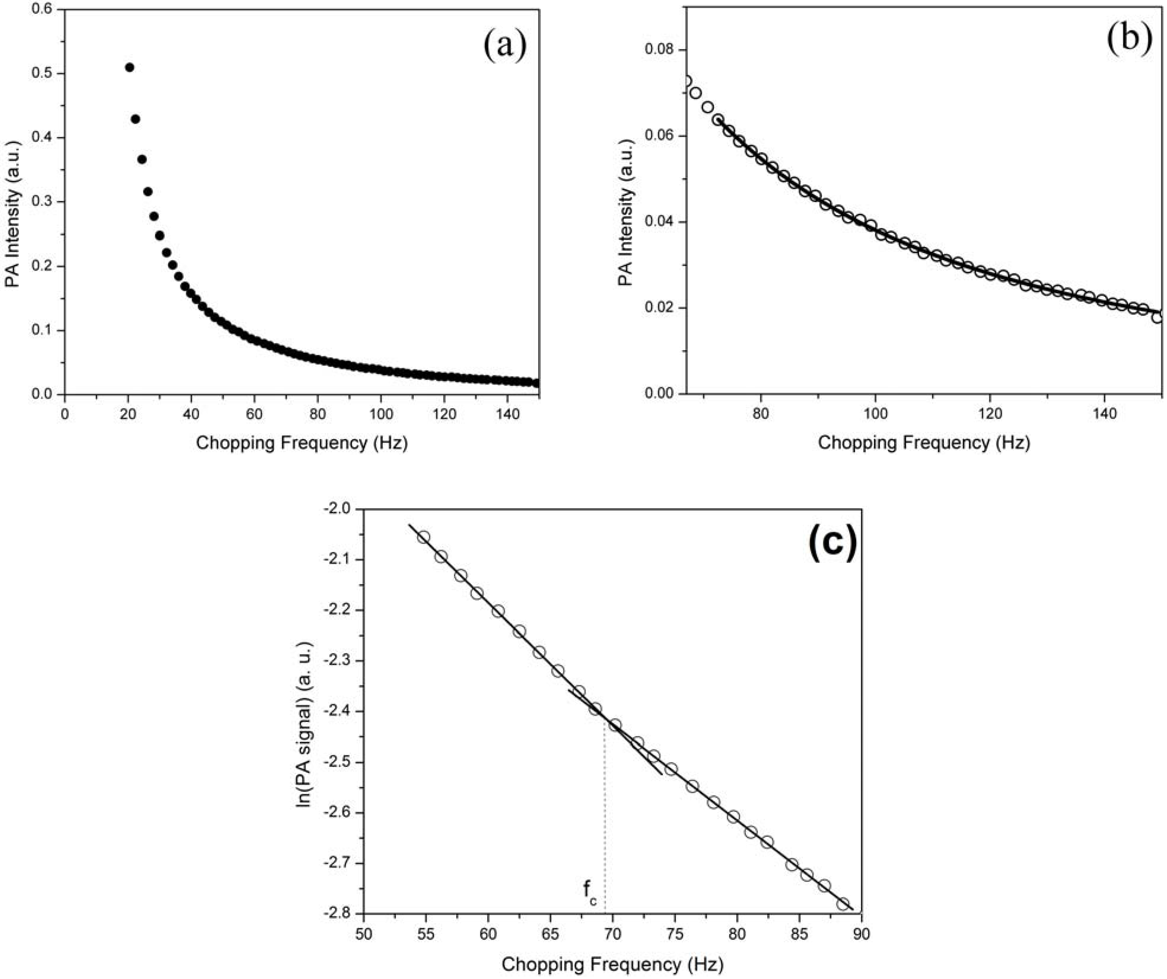
For measuring the TD of samples (αs) the PA signal is plotted versus the chopping frequency. By fitting the PA signal to Equation 6 in the thermally thick area, the TD value can be derived from b as the ls is measured with a micrometer screw gauge. The TD value was also obtained from the characteristic frequency (fc), which is the modulation frequency when it passes from a thermally thin to thermally thick regime and the thermal diffusion length is equal to sample thickness, i.e., [22]. In this method the characteristic frequency (fc) has been found from ln(PA signal) versus chopping frequency graph. The TD can be calculated using the Equation 6.
Figure 4(a) shows the PA signal of the PSi/Si sample at a modulation frequency between 15 to 150 Hz. At low frequency, the thermal diffusion length is larger than the thickness of the samples’ so-called thermally thin regime (µs > ls). By increasing the frequency to a certain point, the thermal diffusion length will equal the sample thickness; this value of the frequency corresponds to the characteristic frequency (fc). By increasing the frequency, it changes to the thermally thick regime [23]. Therefore, the PA signals were fitted with Equation 5 only in the thermally thick area (µs < ls) as shown in Figure 4(b). The ln(PA signal) versus chopping frequency, Figure 4(c), shows a distinct change in slope at the frequency (fc) at which crossover takes place. The TD value was calculated for all samples by finding the characteristic frequency using Equation 6, and the values were also confirmed by this method.
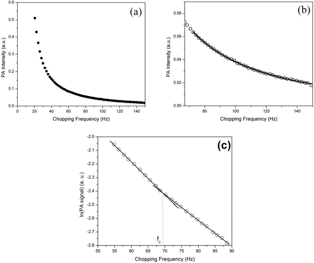
Figure 4.
(a) PA spectra for a sample under a chopping frequency; (b) PA signal versus chopping frequency in the thermally thick regime. The solid curve represents the best fit of the data to Equation 5 in this area; (c) ln(PA signal) versus chopping frequency to find the characteristic frequency (fc).
Before characterising the PSi samples, the optical setup and measuring procedures were tested with a c-Si wafer and the TD values for the four samples were found between 0.84–0.90 cm2/s, in good agreement with values in the literature [24,25,26,27]. This measurement was done for silicon and Au/PSi before and after annealing, and also PSi before annealing, in order to measure and trace the variation of TD in the different conditions of this study.
Figure 5 shows the TD values for silicon annealed at different temperatures. These results were taken freshly after annealing and 30 days after annealing. It is clear that in the first set, the TD of silicon decreases with increasing temperature, but returns to its primary value over time, and shows these values reach 0.84–0.88 cm2/s 30 days after annealing.
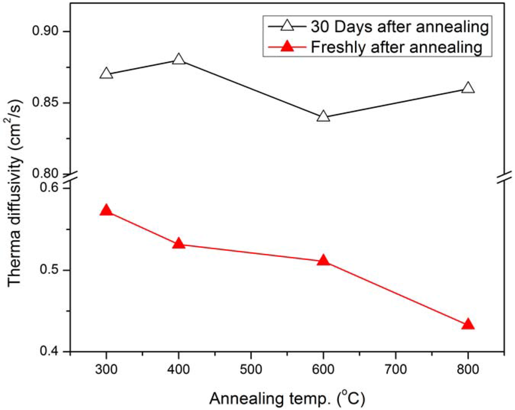
Figure 5.
The TD of the Si for different annealing temperatures for freshly annealed and 30 days after annealing.
Figure 5.
The TD of the Si for different annealing temperatures for freshly annealed and 30 days after annealing.

The variations in the TD value of the PSi and Au/PSi samples before and after annealing are compared in Figure 6 and the values are also shown in Table 1. It is clear that the TD increases gradually by depositing an Au layer on PSi, and then decreases with increasing annealing temperature. Also it decreases with increasing porosity. This value was measured also for the same samples after 30 days and will be described later.

Table 1.
Comparison of the measured values for the TD (cm2/s).
| Sample | Etching time (min) | |||||
|---|---|---|---|---|---|---|
| 10 | 20 | 30 | 40 | 60 | 70 | |
| PSi | 0.693 | 0.580 | 0.563 | 0.553 | 0.522 | 0.505 |
| Au/PSi | 0.710 | 0.644 | 0.609 | 0.596 | 0.564 | 0.551 |
| Au/PSi (at T = 300 °C) | 0.581 | 0.528 | 0.511 | 0.501 | 0.479 | 0.474 |
| Au/PSi (at T = 400 °C) | 0.559 | 0.510 | 0.503 | 0.491 | 0.478 | 0.468 |
| Au/PSi (at T = 600 °C) | 0.526 | 0.490 | 0.480 | 0.466 | 0.450 | 0.438 |
| Au/PSi (at T = 800 °C) | 0.513 | 0.477 | 0.464 | 0.451 | 0.424 | 0.419 |

Figure 6.
Variation of the TD with etching time for all samples. For annealed samples, it was measured exactly after cooling.
Figure 6.
Variation of the TD with etching time for all samples. For annealed samples, it was measured exactly after cooling.
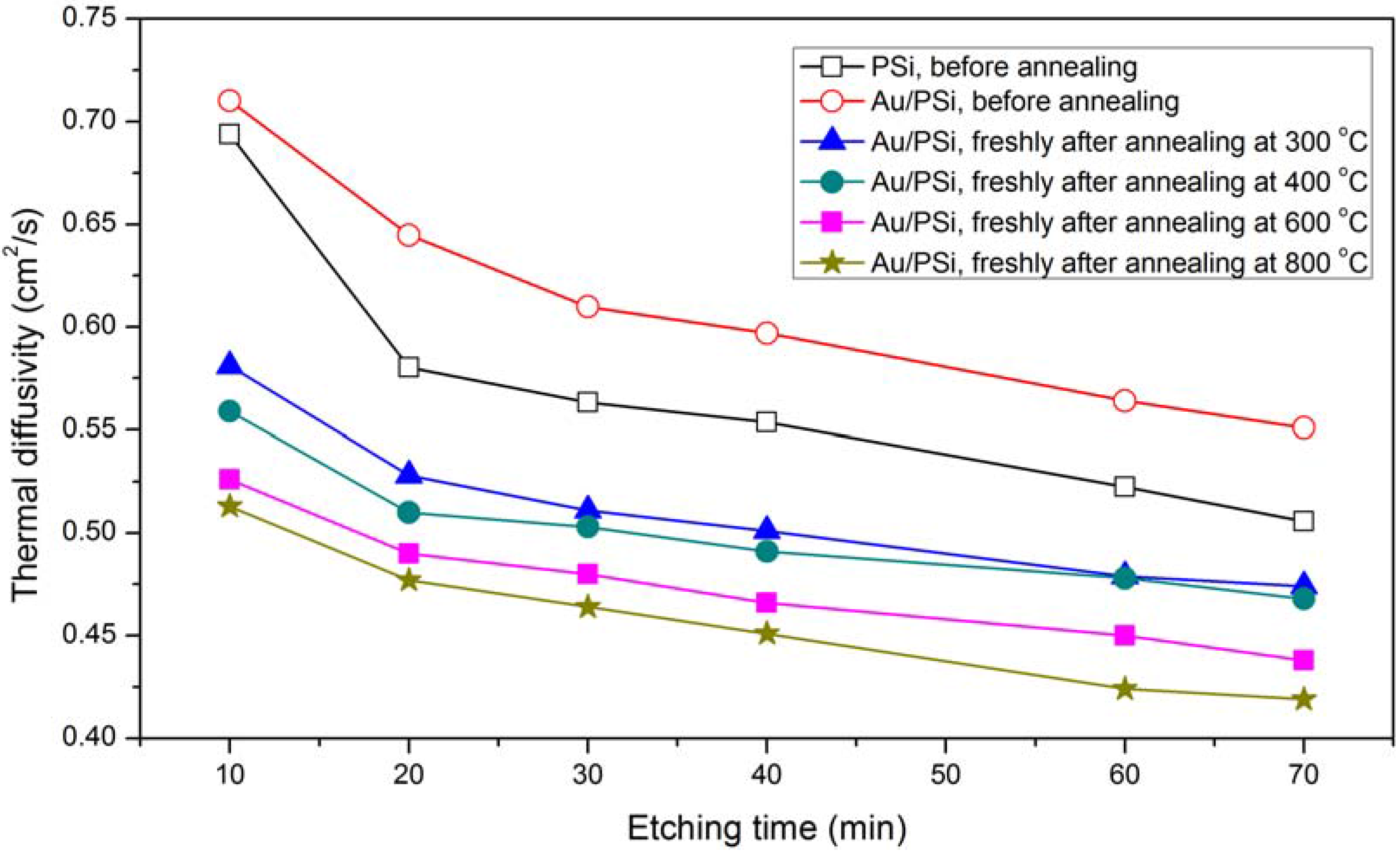
From results of PSi samples, a regular physical trend emerges from the behaviour of signal amplitude: with increasing modulation frequency, and therefore decreasing thermal diffusion length (µs) in the sample, the surface layer has a stronger effect on the thermal transport, and the sample surface temperature progressively increases, as a consequence of the lower thermal conductivity of the layer with respect to that of the Si substrate. The decrease in the TD with increased porosity is a consequence of the decrease in the mean free path, due to the phonon confinement in the crystallites. When the phonon mean free path is less than the crystallite size, phonons are confined, and so the TD is reduced [28,29]. Increasing the TD by depositing an Au layer is due to the additional metal layer itself; with a higher TD than for PSi without an Au layer on the semiconductor substrate. In the next step, annealing the gold coated porous silicon (Au/PSi) samples caused these values to drop slightly, with increased temperature, in the range of the porosities examined. The decrease in the TD means that the thermal conductivity was decreased in the samples that are related to the thermal carrier or media. The thermal carriers are not affected by temperature in this range (300–800 °C), so the decrease in the TD is due to the temporarily deformation of the Si lattice.
The TD was measured for Au/PSi samples 30 days after annealing and was compared with the freshly annealed samples.
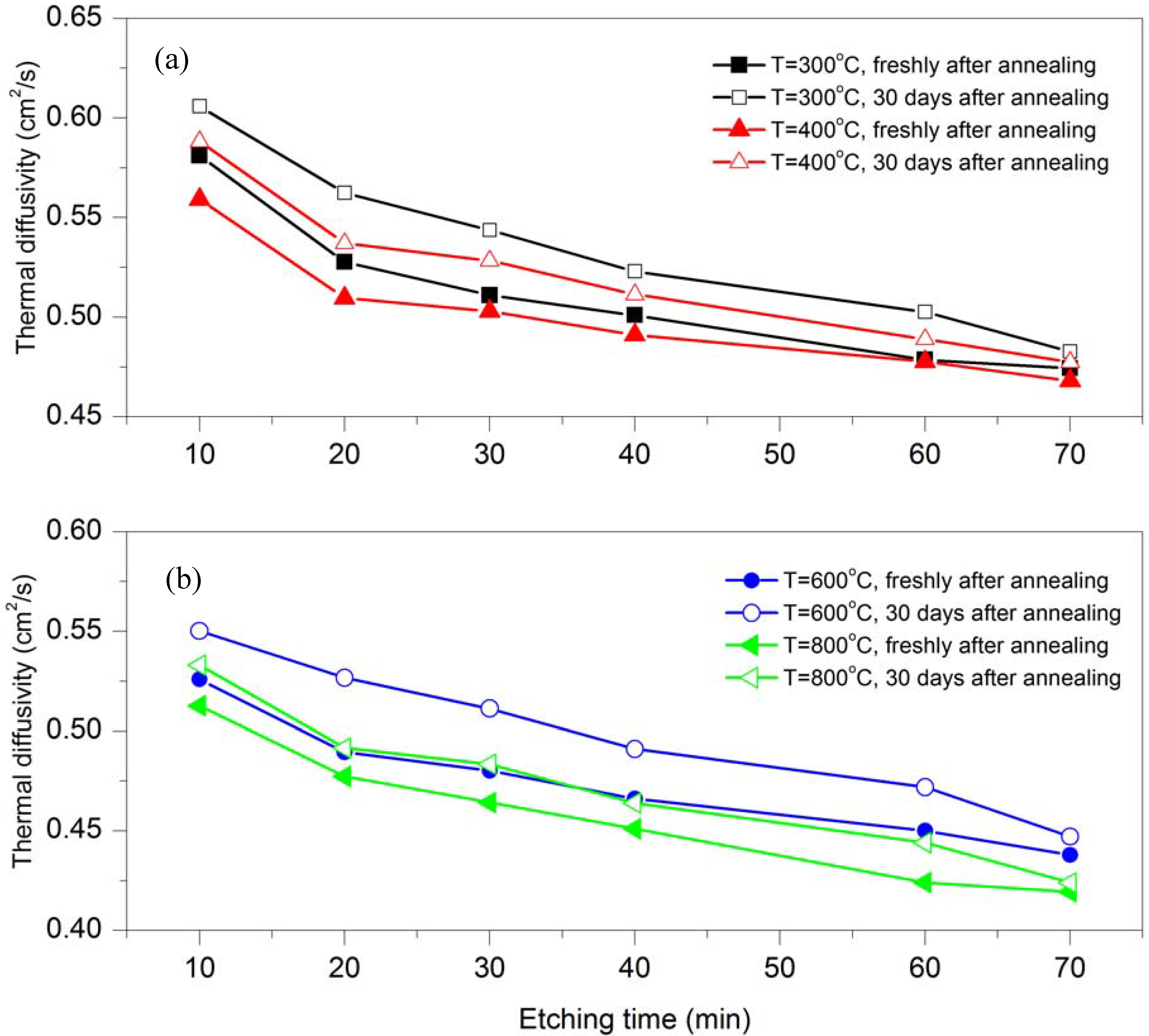
Figure 7 shows four graphs related to different annealing temperatures at 300 °C, 400 °C, 600 °C and 800 °C. Each graph compares the TD for freshly annealed samples and the same samples after 30 days. All four graphs show that the TD decrease on raising the etching time for freshly annealed samples and for samples 30 days after annealing, but the TD for the samples 30 days after annealing increases over time. It is defined as an aging effect in that the TD gradually increases around 2–6% after 30 days. The aging effect is due to a diminished effect of the annealing on lattice deformation.

Figure 7.
Variation of the TD with etching time for Au/PSi samples fresh after annealing and 30 days after annealing at different temperatures (a) T = 300 and 400 °C; (b) T = 600 and 800 °C.
Figure 7.
Variation of the TD with etching time for Au/PSi samples fresh after annealing and 30 days after annealing at different temperatures (a) T = 300 and 400 °C; (b) T = 600 and 800 °C.
3. Experimental Section
3.1. Sample Preparation
All samples were formed on p-type silicon single crystal wafers of 520 μm thickness and resistivity 1–10 ohm·cm, polished on one side. The wafers were cut into rectangular pieces, with the typical area of the pieces being approximately 5 cm2. To provide a uniform current distribution across the surface, an aluminium layer was deposited on the back side of all samples. Each sample was placed on the bottom of a cylindrical Teflon cell and fixed with an aluminium plate as a backing material. The cell consisted of two electrodes, a Si wafer as anode and a platinum rod as cathode, the cathode placed perpendicular to the anode surface. All samples were obtained by varying the etching time, and a constant concentration of HF (48–50%), ethanol (99.90%) and distilled water solution in a volumetric ratio (HF:C2H5OH:H2O) of 1:2:1 was used. Electric current was supplied with an ADCMT 6,243 DC voltage/current source/monitor. Our samples in this study were prepared with 30 mA/cm2 fixed current density and 10, 20, 30, 40, 60, and 70 min anodization times. After anodization a thin semi-transparent Au layer (50–60 nm) was deposited on all samples at room temperature, using a VG Microtech SC7640 sputter coater. The prepared samples were then annealed for one hour at 300, 400, 600 and 800 °C using a tube furnace under argon flow at atmospheric pressure. There are four sets of Au/PSi samples annealed at four different annealing temperatures. Each set consists of one piece of Si wafer that was annealed with the others to use as a reference sample.
3.2. Characterisation
The photoacoustic spectroscopy (PAS) setup consisted of a light source, detector, and data analysing system. A Melles Griot HeNe laser of 632.8 nm at a power of 75 mW was used as a light source, and was modulated by a Stanford Research Systems optical chopper SR540. A handmade open photoacoustic cell (OPC) was used as a detector. A Stanford Research Systems low-noise preamplifier, SR560, was used to amplify the very weak output signal from OPC, which was sent to a Stanford Research Systems lock-in amplifier SR530. A program written in Lab VIEW was used to control the system and collect the data from the lock-in amplifier, via a GPIB bus, Figure 8. The photoacoustic (PA) signal was obtained with chopping frequencies in the range of 10–150 Hz.
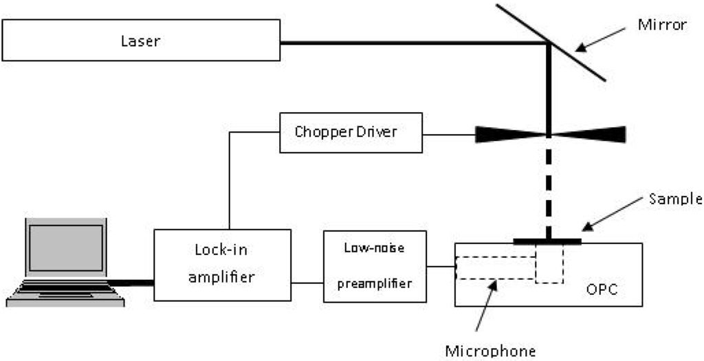
Figure 8.
Schematic diagram of PAS setup.
Figure 8.
Schematic diagram of PAS setup.

4. Conclusions
To conclude, the PAS technique has been used to study the thermal properties of the samples before and after annealing. The Si samples have different TDs based on annealing temperatures and after 30 days the TD of all silicon samples return to their initial values. For PSi/Si samples the layer thickness and porosity increased with etching time and the TD was significantly smaller than that of the Si samples. It decreased with increasing porosity caused by a decrease in the mean free path due to the phonon confinement in the crystallite. The Au/PSi samples show gradually higher values for TD, in the range of porosities examined, because of the deposited metal layer. By annealing the Au/PSi, white spots of gold islands were observed on the PSi surface. The Au was pulled together from the nearest surface to form gold clusters after annealing. In this case, the TD for freshly annealed samples was even smaller than that of the PSi/Si samples and decreased on raising the annealing temperature. Additionally, for the annealed Au/PSi samples, the TD values rose slightly after thirty days. Overall, the TD was decreased by raising the annealing temperature and thus inducing deformations in the lattice. Also aging effect showed a small increase in the TD over time due to the diminished effect of the annealing in the lattice deformation. This indicates that the TD of all samples can be controlled by changing their porosities and annealing temperatures, and then operated as tuneable thermal insulators in silicon based devices or hydrogen fuel cells with the aging effect consideration.
Acknowledgments
We gratefully acknowledge the Department of Physics, UPM for providing the research facilities to enable us to carry out this research. We would also like to acknowledge Ministry of Higher Education for the financial support through Fundamental research grant (01-11-08-664FR/5523664 and 01-04-10-861FR/5523901).
References
- Boit, C.; Lau, F.; Sittig, R. Gold diffusion in silicon by rapid optical annealing. Appl. Phys. A 1990, 50, 197–205. [Google Scholar] [CrossRef]
- Morooka, M. Growth and shrinkage of stacking faults by gold diffusion in silicon. J. Mater. Sci. 1996, 7, 221–225. [Google Scholar]
- Marchal, G.; Mangin, P.; Janot, C. Crystallization of AuxSi1−x amorphous alloys. Philos. Mag. Part B 1980, 42, 81–94. [Google Scholar] [CrossRef]
- Tsaur, B.Y.; Mayer, J.W. Metastable Au-Si alloy formation induced by ion-beam interface mixing. Philos. Mag. A 1981, 43, 345–361. [Google Scholar] [CrossRef]
- Kambli, U.; Allmen, M.; Saunders, N.; Miodownik, A. A comparison of glass forming ability in Ag-Si and Au-Si alloys. Appl. Phys. A 1985, 36, 189–192. [Google Scholar] [CrossRef]
- Calliari, L.; Sancrotti, M.; Braicovich, L. Agglomeration at Si/Au interfaces: A study with spatially resolved Auger line-shape spectroscopy. Phys. Rev. B 1984, 30, 4885–4887. [Google Scholar] [CrossRef]
- Chen, C.R.; Chen, L.J. Morphological evolution of the low-temperature oxidation of silicon with a gold overlayer. J. Appl. Phys. 1995, 78, 919–925. [Google Scholar] [CrossRef]
- Aliyu, Y.H.; Morgan, D.V.; Thomas, H.; Bland, S.W. AlGaInP LEDs using reactive thermally evaporated transparent conducting indium tin oxide (ITO). Electron. Lett. 1995, 31, 1691–1692. [Google Scholar] [CrossRef]
- Charrier, J.; Guendouz, M.; Haji, L.; Joubert, P. Porosity gradient resulting from localised formation of porous silicon: The effect on waveguiding. Phys. Status Solidi A 2000, 182, 431–436. [Google Scholar] [CrossRef]
- Amin-Chalhoub, E.; Semmar, N.; Coudron, L.; Gautier, G.; Boulmer-Leborgne, C.; Petit, A.; Gaillard, M.; Mathias, J.; Millon, E. Thermal conductivity measurement of porous silicon by the pulsed-photothermal method. J. Phys. D 2011, 44, 1–8. [Google Scholar] [CrossRef]
- Nahor, A.; Berger, O.; Bardavid, Y.; Toker, G.; Tamar, Y.; Reiss, L.; Asscher, M.; Yitzchaik, S.; Sa’ar, A. Hybrid structures of porous silicon and conjugated polymers for photovoltaic applications. Phys. Status Solidi C 2011, 8, 1908–1912. [Google Scholar] [CrossRef]
- Rea, I.; Iodice, M.; Coppola, G.; Rendina, I.; Marino, A.; de Stefano, L. A porous silicon-based Bragg grating waveguide sensor for chemical monitoring. Sens. Actuators B 2009, 139, 39–43. [Google Scholar] [CrossRef]
- Chen, C.H.; Chen, Y.F. Strong and stable visible luminescence from Au-passivated porous silicon. Appl. Phys. Lett. 1999, 75, 2560–2562. [Google Scholar] [CrossRef]
- Mimura, H.; Miyajima, K.; Yokoo, K. Electron emission from porous silicon planar emitters. In Papers from the 14th International Vacuum Microelectronics Conference (IVMC2002) and The 48th International Field Emission Symposium (IFES); AVS: Lyon, France, 2003. [Google Scholar]
- Laiho, R.; Pavlov, A. Electronic properties and Schottky barrier of the porous silicon—Au interface. Thin Solid Films 1995, 255, 276–278. [Google Scholar] [CrossRef]
- Hong, C.; Kim, H.; Park, S.; Lee, C. Optical properties of porous silicon coated with ultrathin gold film by RF-magnetron sputtering. J. Eur. Ceram. Soc. 2010, 30, 459–463. [Google Scholar] [CrossRef]
- Adachi, T. Eutectic reaction of gold thin-films deposited on silicon surface. Surf. Sci. 2002, 506, 305–312. [Google Scholar] [CrossRef]
- Bisi, O.; Ossicini, S.; Pavesi, L. Porous silicon: A quantum sponge structure for silicon based optoelectronics. Surf. Sci. Rep. 2000, 38, 1–126. [Google Scholar] [CrossRef]
- Chan, K.; Aspanut, Z.; Goh, B.; Sow, C.; Varghese, B.; Rahman, S.; Abdul Muhamad, M. Effects of post-thermal annealing temperature on the optical and structural properties of gold particles on silicon suboxide films. Appl. Surf. Sci. 2011, 257, 2208–2213. [Google Scholar] [CrossRef]
- Yu, G.Q.; Tay, B. K.; Zhao, Z. W.; Sun, X.W.; Fu, Y.Q. Ion beam co-sputtering deposition of Au/SiO2 nanocomposites. Phys. E 2005, 27, 362–368. [Google Scholar] [CrossRef]
- Rosencwaig, A.; Gersho, A. Theory of the photoacoustic effect with solids. J. Appl. Phys. 1976, 47, 64–69. [Google Scholar] [CrossRef]
- Lima, J.C.D.; Schmitt, M.; Grandi, T.A.; Campos, C.E.M.; Holn, H. Structural and photoacoustic studies of mechanically alloyed Ga40Sb38Se22 powder. J. Phys. 2007, 19, 1–10. [Google Scholar]
- Ramachandran, E.; Raji, P.; Ramachandran, K.; Natarajan, S. Photoacoustic study of the thermal properties of calcium carbonate—The major constituent of pancreatic calculi. Cryst. Res. Technol. 2006, 41, 64–67. [Google Scholar] [CrossRef]
- Sheng, C.K.; Mahmood Mat Yunus, W.; Yunus, W.; Abidin Talib, Z.; Kassim, A. Characterization of thermal, optical and carrier transport properties of porous silicon using the photoacoustic technique. Phys. B 2008, 403, 2634–2638. [Google Scholar] [CrossRef]
- Pinto Neto, A.; Vargas, H.; Leite, N.F.; Miranda, L.C.M. Photoacoustic characterization of semiconductors: Transport properties and thermal diffusivity in GaAs and Si. Phys. Rev. B 1990, 41, 9971–9979. [Google Scholar] [CrossRef]
- Shen, Q.; Toyoda, T. Characterization of thermal properties of porous silicon film/silicon using photoacoustic technique. J. Therm. Anal. Calorim. 2002, 69, 1067–1073. [Google Scholar] [CrossRef]
- Calderon, A.; Munoz Hernandez, R.A.; Tomas, S.A. Method for measurement of thermal diffusivity in solids: Appliction to metals, semiconductors and thin materials. Appl. Phys. 1998, 84, 6327–6329. [Google Scholar] [CrossRef]
- Srinivasan, R.; Jayachandran, M.; Ramachandran, K. Photoacoustic studies on optical and thermal properties of p-type and n-type nanostructured porous silicon for (100) and (111) orientations. Cryst. Res. Technol. 2007, 42, 266–274. [Google Scholar] [CrossRef]
- Zou, J.; Balandin, A. Phonon heat conduction in a semiconductor nanowire. J. Appl. Phys. 2001, 89, 2932–2938. [Google Scholar] [CrossRef]
© 2012 by the authors. Licensee MDPI, Basel, Switzerland. This article is an open access article distributed under the terms and conditions of the Creative Commons Attribution license ( http://creativecommons.org/licenses/by/3.0/).
