Article

Electrically Active Defects and Traps and Their Relation to Stoichiometry and Chemical Environment in HfO2/Al2O3 Dielectric Stacks as Revealed by XPS

1
Institute of Solid State Physics, Bulgarian Academy of Sciences, 72 Tsarigradsko Chaussee, 1784 Sofia, Bulgaria
2
National Centre of Excellence Mechatronics and Clean Technologies, Kl. Ohridski Blvd, 8, Bl. 8, BG-1000 14, 1756 Sofia, Bulgaria
3
Institute of General and Inorganic Chemistry, Bulgarian Academy of Sciences, 1113 Sofia, Bulgaria
4
Institute of Physics, Polish Academy of Sciences, Al. Lotników 32/46, 02-668 Warsaw, Poland
*
Author to whom correspondence should be addressed.
Materials 2025, 18(23), 5420; https://doi.org/10.3390/ma18235420 (registering DOI)
Submission received: 3 November 2025 / Revised: 29 November 2025 / Accepted: 30 November 2025 / Published: 1 December 2025

Abstract

Charge-trapping memory (CTM) is a viable contender to supersede the floating gate technology in high-density flash memory applications. To this end, very reliable charge storage in CTM should be secured. This requires optimization of trap density, their energy and spatial location as well as a deep understanding of their origin. In this work, we used X-ray photoelectron spectroscopy (XPS) to investigate chemical bonds in nanolaminated and doped HfO2/Al2O3 stacks in an effort to gain insight into the nature of defects in the electron/hole trapping processes. The impact of Al incorporation into the HfO2 and rapid thermal annealing (RTA) in O2 on the composition, stoichiometry and bonding configurations was studied. Incorporation of Al into HfO2 leads to an increased concentration of Hf-suboxides. Subsequent RTA effectively reduces suboxides, enhances the stoichiometry of the HfO2/Al2O3 stacks and facilitates intermixing at the dielectric interface, resulting in the formation of Hf–Al–O bonds. The valence band spectra indicate that both Al incorporation and RTA change the dielectric/Si band alignment in a similar way, lowering the valence band offset. The observed changes were considered in relation to the electrically active defects and traps in the structures.

Graphical Abstract

1. Introduction

In recent years, flash memory has emerged as the fastest-growing segment of semiconductor products. To meet the demands of advanced ultra-high-density flash memory architectures, such as 3D-NAND, there is a growing need to replace the conventionally used silicon nitride (Si3N4) with high-k dielectric materials in the current charge-trapping memory (CTM) [1,2,3]. This transition aims to reduce the overall effective oxide thickness of the memory stack, thereby enhancing device performance. Notably, high-k materials have relatively high dielectric constant and large conduction band offsets with Si and tunnel oxide and are known for their trap-rich electronic structure—a characteristic typically considered detrimental in other nanoelectronic applications, such as logic devices [4,5,6]. In the context of CTM, however, the traps can be highly beneficial. A number of requirements for charge traps must be met to fully realize the potential of CTM technology. Specifically, their density, energy levels and spatial distribution should be carefully optimized to minimize leakage and variability, prevent thermal de-trapping and reduce the risk of lateral charge spreading. Moreover, these traps must maintain their characteristics at high temperatures, for long retention times and under cycling stress while exhibiting fast charge capture and emission [7]. Meeting these criteria ensures efficient and reliable charge trapping and storage, as well as fast programming and erasing—key factors for the enhanced performance and endurance of CTM devices. Achieving this requires a deep understanding of the origin of the traps, their energy and spatial distribution and the strategies available to tailor their properties. Viable approaches to modify the trap properties include doping/mixing of high-k dielectrics with other elements, annealing steps, UV irradiation, bandgap engineering, etc. [8,9,10].
Among the promising high-k dielectrics considered as a possible charge-trapping layer in CTM, HfO2-based high-k dielectrics fabricated using atomic layer deposition (ALD) stand out due to the substantial knowledge acquired on their properties and their well-established integration in advanced microelectronic applications. In particular, introducing Al in HfO2 or stacking HfO2 with Al2O3 has been reported to improve the charge-trapping ability and enhance the memory performance and reliability of CTM [11,12,13,14]. In our previous studies [15,16,17,18], we have demonstrated that charge-trapping layers (CTLs) incorporating HfO2/Al2O3 stacks exhibit superior charge-trapping efficiency compared to Si3N4. Moreover, the charge-trapping performance of HfO2/Al2O3 CTLs can be tailored and enhanced through optimization of the stack parameters and annealing processes. In particular, we have investigated CTLs with various Al-layer thickness and number of HfO2/Al2O3 interfaces subjected to RTA in O2 or N2. The results revealed that the annealing in O2 affects stronger the charge-trapping ability of the stacks while the existence of HfO2/Al2O3 interfaces influences it only slightly with nanolaminated stacks demonstrating stronger electron trapping than the doped ones; neither the retention of electrons nor their discharge mechanism or discharge rate depend on the CTL [17]. These results imply that the same type of trap is responsible for electron trapping in both types of CTL, which gives us a reason to conclude that the traps are related to Al2O3 rather than to the number of interfaces. Aluminum introduces deep, high-density traps without increasing leakage currents, while O2 annealing further enhances electron trapping in HfO2/Al2O3 stacks. Consequently, the combination of Al incorporation into HfO2 and O2 annealing yields improved trapping and storage capabilities, reflected in large memory windows as well as excellent retention and endurance of the CT stacks. However, the origin of this improvement is unclear and remains a subject of ongoing investigation.
In this work, the stoichiometry and chemical environment of hafnium in HfO2/Al2O3 stacks and their band alignment with Si were studied by XPS and correlated to oxide charges and traps in the stacks.

2. Materials and Methods

Two types of HfO2-Al2O3 stacks were prepared by ALD: (i) nanolaminated HfO2/Al2O3 and (ii) Al-doped HfO2 (Figure 1). The stacks were deposited on p-type Si (1 0 0) wafers. Prior to the deposition the substrates were chemically cleaned by using the standard Radio Corporation of America (RCA) process. HfO2 and Al2O3 were obtained using the following precursors: tetrakis(dimethylamido)hafnium (TDMAH) for HfO2 and trimethylaluminum (TMA) for Al2O3, while H2O vapor was employed for oxidation. The deposition temperature for the whole stack structure was Tdep = 135 °C. The stack composition for nanolaminated samples is a building block consisting of 20 cycles (cy) HfO2/over 5 cy Al2O3 repeated 5 times. Al-doped stacks were fabricated by 4 cy HfO2/1 cy Al2O3 block repeated 25 times. The overall thicknesses of both types of stacks were kept the same—16.5 nm, estimated by ellipsometric measurements of single HfO2 or Al2O3 layers grown on Si substrates. After deposition, half of the samples were subjected to rapid thermal annealing (RTA) in O2 at 800 °C for 1 min. Additionally, two single 20 nm reference layers of pure HfO2 and Al2O3 were deposited on Si substrate under the same ALD conditions, and half of them were RTA-treated.
It should be noticed that our previous investigations [17] revealed that RTA conducted under the above-mentioned conditions did not inflict any crystallization of the HfO2/Al2O3 stacks.
The X-ray photoelectron spectra were obtained using Al Kα (1486.6 eV) radiation in a VG ESCALAB MK II hemispherical electron spectrometer under a base pressure of 1 × 10⁻⁸ Pa. The spectrometer resolution was calculated from the Ag 3d5/2 line with the analyzer transmission energy of 20 eV. The full width at half maximum (FWHM) of this line was 1 eV. The spectrometer was calibrated against the Au 4f7/2 line (84.0 eV), and the sample charging was estimated from C 1s (285 eV) spectra from natural hydrocarbon contaminations on the surface. The measurement statistics (signal-to-noise ratio and energy step) allowed a binding energy (BE) accuracy of 0.2 eV to be achieved. The C 1s, O 1s, Al 2p, Si 2p, Hf 4f and Hf 4d core levels as well as the valence band (VB) regions were recorded at a normal take-off angle (90° to the surface). The take-off angle refers to the angle between the emitted photoelectrons (practical photoelectron detector position) and the sample surface. In the current study a take-off angle of 90° (normal emission) was used to ensure maximum sampling depth for maximum signal strength from thinner Al2O3 sublayers, which were placed under thicker HfO2 ones (see Figure 1). The photoelectron spectra were recorded and corrected by subtracting a Shirley-type background and quantified using the peak area and Scofield’s photoionization cross-sections [19]. For the fitting of the Hf 4f and O 1s peaks, a 30% Lorentz–Gauss peak shape was used. The O 1s peak was fitted with a single component, whereas the Hf 4f peak was fitted as a doublet with a spin–orbit splitting of 1.7 eV and an area ratio of 4:3. Peak fitting was performed using XPSPEAK4.1 software, where the resulting fitting error is given by the chi factor, which should ideally be equal to 1.
In order to elucidate possible relations between the chemical structure and the charge states in the investigated HfO2/Al2O3 stacks, MOS capacitors were prepared employing Al metallization. The Al-gate (top) electrode and Al-back contact to Si were deposited by evaporation with subsequent pattering of the gate by photolithography (gate area of 10−4 cm2). The charged defects present in the stacks were estimated through the high-frequency capacitance-voltage technique. The C-V characteristics were measured at room temperature using an Agilent E4890A LCR meter (Keysight, Santa Rosa, CA, USA) in a bias range from 2 V to −8 V at 1 MHz to ensure well pronounced saturation in inversion and accumulation regions. The voltage at which the measured capacitance equals the theoretical flat-band capacitance calculated using the Si doping level and the accumulation capacitance following [20] was designated as the flat-band voltage Vfb.

3. Results

3.1. XPS Study

XPS measurements were used to determine the chemical composition and bonding of as-deposited and annealed dielectric stacks. In Figure 2 the Hf 4f core level spectra for all samples (pure HfO2, laminated HfO2/Al2O3 and doped HfO2/Al2O3 stacks) before (Figure 2a) and after RTA (Figure 2b) are shown. Each Hf 4f spectrum was deconvoluted in two sets of double-peak components. Gaussian–Lorentzian line shapes were used for deconvolution of the spectra after standard Shirley background subtraction. The first doublet peaks are situated at BE of around 17.5 eV and 19.2 eV and correspond to the Hf4+ 4f7/2 and Hf4+ 4f5/2 energy levels of the stoichiometric HfO2 in which hafnium occurs in the 4+ oxidation state (Hf4+) [21]. The second doublet is shifted to lower BE and occurs at 16.9 eV and 18.6 eV, which corresponds to the 4f7/2 and 4f5/2 electronic states of Hf x+ (x < 4) of the Hf suboxide [22,23]. The spin–orbit splitting of 1.7 eV is consistent with the usually reported value for the Hf 4f7/2 and Hf 4f5/2 doublet [24]. In Table 1 the positions of Hf4+ 4f7/2 and Hfx+ 4f7/2 energy levels and their FWHM for all stacks before and after annealing are summarized. No significant differences in the energy position of the stoichiometric and suboxide counterparts of the Hf 4f peak between the stacks are observed. After RTA, a small shift of 0.2 eV toward lower BE for the nanolaminated stack and pure HfO2 is observed. The FWHM also remains almost unchanged after RTA, revealing no increase in the disorder or changes in the amorphous/crystalline status of the films.
As seen in Figure 2a for the as-deposited pure HfO2 layer, the peak associated with the stoichiometric oxide bonds dominates the Hf 4f spectrum. On the contrary, for the as-deposited HfO2/Al2O3 stacks—both nanolaminated and doped ones—the low BE doublet dominates the Hf 4f spectra, i.e., Al inclusion increases Hf-suboxides (Figure 2a). The latter is in accordance with the results in [25] showing that Al-doping decreases the formation energy of oxygen vacancies caused by the Al substitution for Hf. Moreover, Al as a trivalent element is believed to form ionically compensated (2AlHf)Vo and mixed compensated AlHfVo defects consisting of negatively charged Al ions and double positively charged oxygen vacancies. Interstitial Al could also lead to the formation of oxygen vacancies. The (2AlHf)VO defect has lower formation energy than the AlHfVO defect under both oxygen-rich and oxygen-poor conditions. Nevertheless, the AlHfVO defect might still form under oxygen-poor conditions since it does not require special placement of dopant atoms, unlike the (2AlHf)VO defect, which depends on a next-next-neighbor configuration of dopants and vacancy. The formation energy of an interstitial Al defect complex with oxygen vacancy is higher than that of (2AlHf)VO and AlHfVO [26]. After RTA, a significant increase in the Hf 4f peak corresponding to stoichiometric Hf4+ is observed in both nanolaminated and doped stacks, and its intensity is higher than that of the sub-stoichiometric one. Therefore, it can be assumed that RTA reduces the number of suboxides and improves the stoichiometry of HfO2/Al2O3 stacks. This is very well demonstrated in Table 1, where the area ratios of the Hf 4f peaks of stoichiometric and substoichiometric oxide components before and after RTA are also given. For doped stacks this ratio increases from 0.55 for the as-deposited to 1.53 for the annealed sample, i.e., by almost three times. As seen, there is also some improvement for the pure HfO2; however, the increase is insignificant (from about 1.7 to 1.9 after RTA).
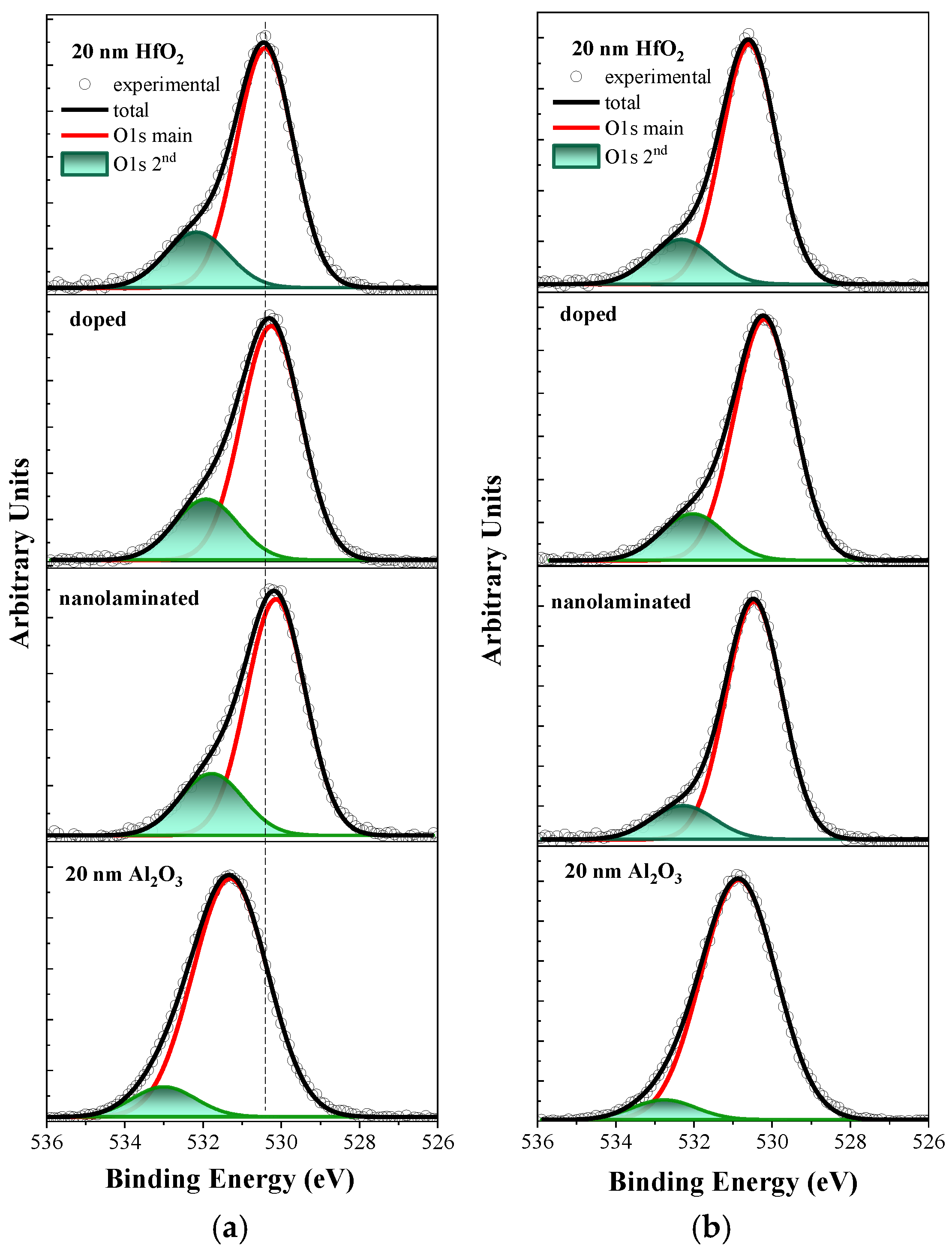
In Figure 3 the O 1s spectra of pure HfO2, Al2O3 layers and HfO2/Al2O3 stacks are presented. For HfO2 and HfO2/Al2O3 stacks, O 1s spectra are fitted by two Gauss–Lorenzian peaks: the main one corresponding to Hf-O bonds at 530.1–530.4 eV and the second one at about 532 eV. The main O 1s contribution of the reference Al2O3 corresponding to Al-O bonds is positioned at higher BE of 531.30 eV, which is higher compared to the O 1s peak of the Hf-O bonds. The positions of the two O 1s peaks for all samples before and after RTA are given in Table 2. The O 1s peak position of the two HfO2/Al2O3 stacks is shifted by about 0.2–0.3 eV toward lower BE compared to the O 1s line of pure HfO2, which might be assigned to their sub-stoichiometric composition. The second O 1s peak located at 532.15 eV in pure HfO2 is usually associated with interstitial oxygen, oxygen vacancies, −OH bonds [24] or residual surface contaminants (e.g., C-O bonds) [27]. As seen (Table 2) this peak is shifted to lower BE for the two HfO2/Al2O3 stacks compared to pure HfO2. After RTA (Figure 3b, Table 2), the O 1s peak positions of pure HfO2 and doped stacks remain largely unaffected (a slight shift of about 0.1–0.2 eV to higher BE is observed). For the nanolaminated stack the shifts are slightly larger—0.3 eV to higher BE for the main O 1s peak shifts and 0.5 eV for the second O 1s peak.
In Table 2 the O 1s (main Me-O peak)/O 1s(second peak) ratio is also given. For the as-deposited pure HfO2 and Al2O3 films, this ratio is higher, which reflects their better stoichiometry and reduced defects. After RTA, the O 1s (main Me-O peak)/O 1s (second peak) ratio increases in all samples. The improved ratio can be explained with the reduced contribution from O vacancies, -OH bonds and C-O bonds after annealing. It is known that O2 RTA eliminates C, for example, in hafnium silicate (HfSiO) thin films [28].
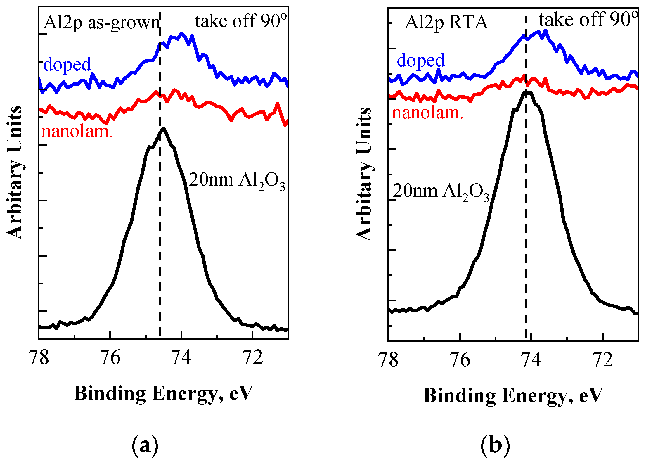
The Al 2p core level spectra are shown in Figure 4. A single Gaussian line is used to fit the Al 2p peak as the spin–orbit splitting of Al 2p peak from Al2O3 is negligible. The Al 2p core level of both HfO2/Al2O3 stacks exhibits a shift of approximately 0.2–0.3 eV toward lower BE, indicating the formation of Hf–Al–O bonds [29,30]. This shift is better pronounced for the doped layers because of the larger number of HfO2/Al2O3 interfaces, which suggests a larger number of Hf-Al-O bonds. It should be noted, however, that the conjugated shift of the Hf 4f doublet with 0.2–0.3 eV toward higher BE compared to its position for “pure” HfO2 [29,31,32] is not observed. Considering the information depth of approximately 5 nm for the XPS method, the reduced intensity of the Al 2p peak in the nanolaminated stack can be readily explained by the position of the Al2O3 sublayer, located about 2.5 nm beneath the surface. After RTA, position of the Al 2p peak in the pure Al2O3 shifts by about 0.4 eV to lower BE. Several works have reported a similar shift of the Al 2p peak toward lower BE after thermal annealing [33,34]. Such a shift of the Al 2p peak at higher processing temperatures is mainly attributed to the decrease in the concentration of OH ions or coordination number of Al3+ ions in the film. The shift of the Al 2p peak in doped and laminated stacks after RTA is less pronounced, but its position remains at lower energies compared to that of the pure Al2O3.
Valence band spectra were also investigated (Figure 5) to reveal the band alignments in different structures. To this end, the Hf 5d peak located at about 7.5 eV was measured. The valence band edge of oxide layer, Ev(ox), was determined by linear extrapolation of the leading edge to the baseline of the valence band spectra. The valence band edge of dielectric layers before and after RTA are summarized in Table 3. Considering the valence band energy of Si, Ev(Si), which is approximately 0.24 eV below the Fermi level (based on the substrate dopant concentration and the data in [35]), the valence band offset at the dielectric/Si interface, ΔEv, can be estimated as the difference between the valence band edges of the dielectric and of Si. A more precise determination of valence band offsets can be obtained by Kraut et al.’s equation [36]; however, this requires additional data. Nevertheless, the ΔEv values obtained here are in good agreement with reported data [37]. The largest ΔEv—3.31 eV—is observed for pure HfO2. Al introduction in the stacks results in a decrease in ΔEv, and this reduction is stronger for the doped stack. A noticeable reduction in ΔEv is observed after oxygen annealing for pure HfO2 and laminated stacks. For doped stacks, the reduction is smaller and could be considered within the experimental error. Therefore, both Al incorporation and RTA in O2 similarly influence the valence band offset at the dielectric/Si interface by decreasing its value.

3.2. Charges in the Stacks

Electrically active defects in the stacks were investigated by measuring the C-V curves (Figure 6). The density of the initial oxide charge, denoted as Qf, is determined from the flatband voltage (Vfb) extracted from the C-V curves. The flatband voltage corresponds to the applied voltage at which the capacitance equals the flatband capacitance. This capacitance is defined by the doping concentration of the Si and the capacitance of the dielectric stack. The relationship between Vfb and Qf is given by [20]:
V fb =   φ ms Q f / C 0 ,
where C0 is the capacitance in accumulation and φms is the metal–semiconductor work function difference. (The Al work function of 4.25 eV is used in calculations.) The value of Qf is a net oxide charge and includes the charges in the high-k stack as well as the charges at the Si interface and the interfacial layer.
A hysteresis of the flat-band voltage Vfb when performing the C-V measurement from inversion to accumulation and back from accumulation to inversion is also detected. The C-V curves are nearly parallel to each other, revealing that the hysteresis of Vfb is mostly due to traps located within a tunneling distance from the interface that can easily communicate with the Si substrate by tunneling of electrons or holes and in this way changing their charge state and giving rise to the flat-band voltage shift. These traps are usually called “slow” or “border” traps [38], and their density can be approximately calculated by the following equation:
Q sl = Δ V fb C 0 ,
where ΔVfb is the hysteresis. It should be mentioned that the hysteresis gives only the lowest limit for the density of slow states [38]. Considering that a bias of up to −8 V was applied during the measurements to achieve accumulation saturation of the capacitance, at least part of the observed hysteresis could also be attributed to trapping/de-trapping processes in the bulk of the HfO2-based stacks.
The values of Qf, ΔVfb and Qsl for different stacks before and after RTA are given in Table 4. As seen, Qf in HfO2 is positive, and its density is relatively high—3.5 × 1012 cm−2. Introduction of Al in HfO2 reduces Qf significantly (by approximately three times) to 1.1–1.4 × 1012 cm−2. A similar strong reduction is also observed for the C-V hysteresis, which decreases from 3.2 V for the pure HfO2 to 1.2–1.5 V in the HfO2/Al2O3 stacks. The decrease in both Qf and Qsl is stronger for the nanolaminated stack. The large hysteresis of the C-V curves reveals that during the measurement, a large number of injected holes are trapped at the tunneling distance from the interface. The number of hole traps is significantly reduced in the Al-containing stacks. Therefore, it can be concluded that introduction of Al passivates defects in HfO2 and at the interface with Si, thus leading to a substantial decrease in Qf and Qsl. A similar reduction in the hysteresis by Al introduction in HfO2 has also been observed by other authors [39]. Another explanation may be related to the compensation of the oxide charges associated with Al2O3 and HfO2 as the existence of negative oxide charge in thin Al2O3 films has been reported. In fact, the Al dopant in HfO2 (Hf substitution) is expected to act as a shallow acceptor center close (0.093 eV) to the valence band [40] occupied by an electron and hence is negatively charged. The Al substitution for Hf is expected to interact with neighbor oxygen vacancies and passivate them [40]. It should also be noted that the nature of oxygen vacancy in hafnia is quite complex; it could have multiple charge states, both negative and positive depending on the position of the Fermi level.
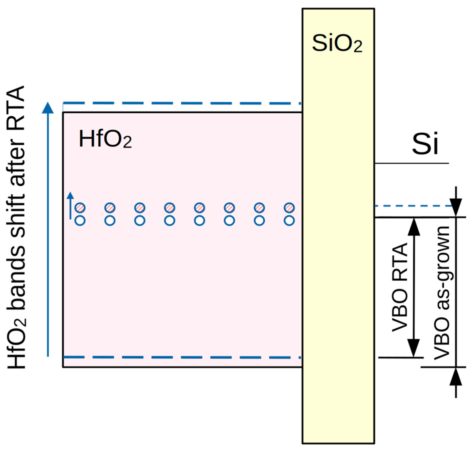
After RTA, Qf remains mostly unaffected in the pure HfO2 and doped stacks, while it increases for the nanolaminated HfO2/Al2O3 stack, reaching the value of the pure HfO2. Taking into account the substantial decrease in suboxides in all stacks after RTA, it can be concluded that they are not the origin of the oxide charge. The hysteresis decreases substantially in all the layers, i.e., RTA in O2 reduces the density of slow traps. The reduction is most notable for pure HfO2, reaching one order of magnitude. This allows us to conclude that the origin of slow traps could be assigned to defects in HfO2. The increase in Qf in nanolaminated stacks after RTA might be related to the change in the band diagram of the stacks and the reduction in the valence band offset at the dielectric/Si interface ΔEv (Table 3). The shift upward of Ev(ox) with respect to Ev(Si) changes the position of traps with respect to the Si valence band. Their energy position aligns with the Si bandgap; hence, they are inaccessible from the Si valence band. In this case, the donor type traps manifest as a fixed positive charge (Figure 7). This also explains the unchanged value of Qf for the doped stack as its change in ΔEv is very small. The suggestion that the increased value of Qf in nanolaminated stacks after RTA is due to the change in their energy position with respect to the Si valence band is supported also by the fact that the sum of Qf and Qsl before and after RTA is approximately equal, e.g., part of Qsl converts into Qf after RTA as a result of the change in the band gap alignment between the high-k stack and Si. This suggestion is supported by a recent paper [41] which investigates the energy position of different oxygen vacancy configurations in HfO2 and finds the energy position of one of these configurations to be about 2.02 eV below the conduction band of HfO2 almost aligned with the Si valence band.
An interesting question that arises from the presented data is on the origin of increased electron trapping in HfO2/Al2O3 stacks after RTA as reported in our previous investigations [16,17]. There are several factors that affect electron trapping at programming voltages (+Vg) in the memory capacitors. The first is the density of electron traps. In HfO2, oxygen vacancies (most likely negatively charged ones, i.e., acting as acceptor levels [42] because they are situated in the upper half of HfO2 bandgap) are considered the main electron traps. Another alternative is the interstitial oxygen (which is related to the oxygen vacancies) that forms a deep acceptor level, but its position in the stable −2 charge state is 0.7 eV below the VB of Si [43]. The results here, however, suggest that the density of oxygen vacancies is reduced after the oxygen annealing. So, the more efficient electron trapping can be explained if we assume that the main trap sites are not the oxygen vacancies but Al-related defect states which increase/emerge after RTA, or alternatively the explanation could be derived from the effects as Coulombic repulsion. The Al-related trap sites are likely to form at HfO2/Al2O3 interfaces [11], especially after RTA. The smearing of HfO2/Al2O3 interfaces was clearly visible on TEM images after annealing [17]; however, this approach would lead to a clear effect of the number of HfO2/Al2O3 interfaces on the memory windows, which is not supported by our data [17]. The decrease in the C-V hysteresis upon annealing favors the repulsion hypothesis as high trap density close to the Si interface and subsequent electron trapping inevitably reduces the injection electric field and hence the tunneling current and the number of injected electrons in the stack. (The electrons trapped at and very near to the interface are lost after the programming voltage cut-off and do not contribute to stable memory window.) The second factor is the capture cross-section and energy level of the traps, and it may be suggested that annealing inflicts some changes in the nature of the traps such as close environment reconstruction that ease the trapping and produce high memory windows despite the decreased density. The third factor that could affect the number of trapped electrons is the level of the Fowler–Nordheim injection current. In the used capacitor configuration, i.e., p-type Si (corresponding to n-channel MOSFET), during the program voltage pulse, Si is in inversion. In this condition the current from the substrate to the stack is limited by the availability of the electrons (minority carriers) in the inversion layer, which in turn is maintained by thermal generation. Therefore, enhanced memory windows of RTA samples might be related to the increased generation rate due to changes in the Si surface region, which are not clear at the moment, but some results infer that such processes could take place [17].

4. Conclusions

The XPS study reveals that incorporation of Al into HfO2 results in an increased concentration of Hf-suboxides, which can be attributed to the reduced formation energy of oxygen vacancies induced by the substitution of Hf atoms with Al. The rapid thermal annealing in O2 enhances the stoichiometry of the HfO2/Al2O3 stacks and facilitates intermixing at the dielectric interface, resulting in the formation of Hf–Al–O bonds, as evidenced by the evolution of Al 2p core-level spectra. The incorporation of Al into HfO2 results in a pronounced reduction in both oxide charge (Qf) and slow trap charge (Qsl), which can be attributed to the passivation of defects within the HfO2 layer and at the HfO2/Si interface. This defect passivation also leads to a substantial decrease in the number of hole traps in the Al-containing stacks. The obtained results imply that suboxides are not the primary source of oxide charge. Moreover, RTA in O2 effectively decreases the density of slow traps, with the most pronounced effect observed for pure HfO2, where a reduction of nearly one order of magnitude is achieved. This finding supports the assignment of slow traps to defects intrinsic to HfO2. The reduction in the valence band offset (ΔEv) between the dielectric and the Si substrate inflicted by both the Al incorporation and the post-deposition RTA in O2 may also affect the electrical behavior of traps. The enhanced electron trapping observed in O2-annealed stacks can be rationalized by assuming that the dominant trap states are not oxygen vacancies but rather Al-related defect states, which either increase in density or become activated during RTA.

Author Contributions

Conceptualization, A.P. and D.S.; formal analysis, D.S., I.A., A.P. and E.G.; investigation, I.A., D.S. and W.W.; resources, I.A., D.S., W.W. and E.G.; data curation, D.S.; writing—original draft preparation, A.P.; writing—review and editing, D.S., E.G. and I.A.; visualization, D.S., A.P. and E.G.; supervision, A.P.; project administration, A.P.; funding acquisition, A.P. All authors have read and agreed to the published version of the manuscript.

Funding

European Regional Development Fund under “Research Innovation and Digitization for Smart Transformation” program 2021–2027 under Project BG16RFPR002-1.014-0006 “National Centre of Excellence Mechatronics and Clean Technologies”. The project was also partially supported by the joint research project between Institute of Solid State Physics, Bulgarian Academy of Sciences and Institute of Physics, Polish Academy of Sciences (2024–2025), under the project IC-PL/03/2024-2025.

Data Availability Statement

The original contributions presented in this study are included in the article. Further inquiries can be directed to the corresponding author.

Conflicts of Interest

The authors declare no conflicts of interest.

Abbreviations

The following abbreviations are used in this manuscript:
CTMCharge-Trapping Memory
CTLCharge-Trapping Layer
RCARadio Corporation of America
RTARapid Thermal Annealing
BEBinding Energy
FWHMFull Width at Half Maximum
VBValence Band
VBOValence Band Offset
C-VCapacitance–Voltage
MOSMetal Oxide Semiconductor

References

  1. Zhao, C.; Zhao, C.Z.; Taylor, S.; Chalker, P.R. Review on Non-Volatile Memory with High-k Dielectrics: Flash for Generation Beyond 32 nm. Materials 2014, 7, 5117–5145. [Google Scholar] [CrossRef] [PubMed]
  2. Hwang, C.S. Prospective of Semiconductor Memory Devices: From Memory System to Materials. Adv. Electron. Mater. 2015, 1, 1400056. [Google Scholar] [CrossRef]
  3. Ramkumar, K. Charge trapping NVMs with metal oxides in the memory stack. In Metal Oxides for Non-Volatile Memory: Materials, Technology and Application; Dimitrakis, P., Valov, I., Tappertzhofen, S., Eds.; Elsevier: Amsterdam, The Netherlands, 2022; pp. 79–107. [Google Scholar]
  4. Houssa, M.; Pantisano, L.; Ragnarsson, L.; Degraeve, R.; Schram, T.; Pourtois, G.; De Gendt, S.; Groeseneken, G.; Heyns, M.M. Electrical properties of high-κ gate dielectrics: Challenges, current issues, and possible solutions. Mater. Sci. Eng. R 2006, 51, 37–85. [Google Scholar] [CrossRef]
  5. Luo, W.; Yuan, T.; Kuo, Y.; Lu, J.; Yan, J.; Kuo, W. Charge trapping and dielectric relaxation in connection with breakdown of high-k gate dielectric stacks. Appl. Phys. Lett. 2006, 88, 202904. [Google Scholar] [CrossRef]
  6. Duschl, R.; Kerber, M.; Avellan, A.; Jakschik, S.; Schroeder, U.; Kudelka, S. Reliability aspects of Hf-based capacitors: Breakdown and trapping effects. Microelctron. Reliab. 2007, 47, 497–500. [Google Scholar] [CrossRef]
  7. Dimitrakis, P. Charge-Trapping Non-Volatile Memories; Dimitrakis, P., Ed.; Springer: Cham, Switzerland, 2015. [Google Scholar]
  8. Spiga, S.; Driussi, F.; Lamperti, A.; Congedo, G.; Salicio, O. Effects of Thermal Treatments on the Trapping Properties of HfO2 Films for Charge Trap Memories. Appl. Phys. Express 2012, 5, 021102. [Google Scholar] [CrossRef]
  9. Kim, J.; Kim, J.; Cho, E.C.; Yi, J. Analysis of HfO2 Charge Trapping Layer Characteristics After UV Treatment. ECS J. Solid State Sci. Technol. 2021, 10, 044003. [Google Scholar] [CrossRef]
  10. Zhu, C.; Huo, Z.; Xu, Z.; Zhang, M.; Wang, Q.; Liu, J.; Long, S.; Liu, M. Performance Enhancement of Multilevel Cell Nonvolatile Memory by Using a Bandgap Engineered High-k Trapping Layer. Appl. Phys. Lett. 2010, 97, 253503. [Google Scholar] [CrossRef]
  11. Lan, X.; Ou, X.; Cao, Y.; Tang, S.; Gong, C.; Xu, B.; Xia, Y.; Yin, J.; Li, A.; Yan, F.; et al. The effect of thermal treatment induced inter-diffusion at the interfaces on the charge trapping performance of HfO2/Al2O3 nanolaminate- based memory devices. J. Appl. Phys. 2013, 114, 044104. [Google Scholar] [CrossRef]
  12. Cui, Z.; Xin, D.; Kim, T.; Choi, J.; Cho, J.; Yi, J. Improvement of the Charge Retention of a Non-Volatile memory by a Bandgap Engineered Charge Trap Layer. ECS J. Solid State Sci. Technol. 2021, 10, 125002. [Google Scholar] [CrossRef]
  13. Hou, Z.; Wu, Z.; Yin, H. The Effect of Thermal Treatment Induced Performance Improvement for Charge Trapping Memory with Al2O3/(HfO2)0.9(Al2O3)0.1/Al2O3 Multilayer Structure. ECS J. Solid State Sci. Technol. 2018, 7, Q229. [Google Scholar] [CrossRef]
  14. Yoon, G.; Kim, T.; Agrawal, K.; Kim, J.; Park, J.; Kim, H.H.; Cho, E.C.; Yi, J. Optimization of MIS type Non-volatile Memory Device with Al-doped HfO2 as Charge Trapping Layer. ECS J. Solid State Sci. Technol. 2020, 9, 075004. [Google Scholar]
  15. Paskaleva, A.; Rommel, M.; Hutzler, A.; Spassov, D.; Bauer, A.J. Tailoring the Electrical Properties of HfO2 MOS-Devices by Aluminum Doping. ACS Appl. Mater. Interfaces 2015, 7, 17032–17043. [Google Scholar] [CrossRef] [PubMed]
  16. Spassov, D.; Paskaleva, A.; Krajewski, T.A.; Guziewicz, E.; Luka, G.; Ivanov, T. Al2O3/HfO2 Multilayer High-k Dielectric Stacks for Charge Trapping Flash Memories. Phys. Status Solidi (A) 2018, 215, 1700854. [Google Scholar] [CrossRef]
  17. Spassov, D.; Paskaleva, A.; Guziewicz, E.; Wozniak, W.; Stanchev, T.; Ivanov, T.; Wojewoda-Budka, J.; Janusz-Skuza, M. Charge Storage and Reliability Characteristics of Nonvolatile Memory Capacitors with HfO2/Al2O3-Based Charge Trapping Layers. Materials 2022, 15, 6285. [Google Scholar] [CrossRef]
  18. Spassov, D.; Paskaleva, A. Challenges to Optimize Charge Trapping Non-Volatile Flash Memory Cells: A Case Study of HfO2/Al2O3 Nanolaminated Stacks. Nanomaterials 2023, 13, 2456. [Google Scholar] [CrossRef] [PubMed]
  19. Scofield, J.H. Hartree-Slater subshell photoionization cross-sections at 1254 and 1487 eV. J. Electron Spectrosc. Rel. Phenom. 1976, 8, 129–137. [Google Scholar] [CrossRef]
  20. Schroder, D.K. Semiconductor Material and Device Characterization, 3rd ed.; John Wiley & Sons, Inc.: Hoboken, NJ, USA, 2006; Chapter 6; p. 328. [Google Scholar]
  21. Manikanthababu, N.; Dhanunjaya, M.; Nageswara Rao, S.V.S.; Pathak, A.P. SHI induced effects on the electrical and optical properties of HfO2 thin films deposited by RF sputtering. Nucl. Instrum. Methods Phys. Res. Sect. B Beam Interact. Mater. At. 2016, 379, 230–234. [Google Scholar] [CrossRef]
  22. Tan, T.; Guo, T.; Wu, Z.; Liu, Z. Charge transport and bipolar switching mechanism in a Cu/HfO2/Pt resistive switching cell. Chin. Phys. B 2016, 25, 117306. [Google Scholar] [CrossRef]
  23. Zhang, W.; Kong, J.-Z.; Cao, Z.-Y.; Li, A.-D.; Wang, L.-G.; Zhu, L.; Li, X.; Cao, Y.-Q.; Wu, D. Bipolar Resistive Switching Characteristics of HfO2/TiO2/HfO2 Trilayer-Structure RRAM Devices on Pt and TiN-Coated Substrates Fabricated by Atomic Layer Deposition. Nanoscale Res. Lett. 2017, 12, 393. [Google Scholar] [CrossRef]
  24. Luo, X.; Li, Y.; Yang, H.; Liang, Y.; He, K.; Sun, W.; Lin, H.-H.; Yao, S.; Lu, X.; Wan, L.; et al. Investigation of HfO2 Thin Films on Si by X-ray Photoelectron Spectroscopy, Rutherford Backscattering, Grazing Incidence X-ray Diffraction and Variable Angle Spectroscopic Ellipsometry. Crystals 2018, 8, 248. [Google Scholar] [CrossRef]
  25. Zhang, H.; Gao, B.; Yu, S.; Lai, L.; Zeng, L.; Sun, B.; Liu, L.; Liu, X.; Lu, J.; Han, R.; et al. Effects of Ionic Doping on the Behaviors of Oxygen Vacancies in HfO2 and ZrO2: A First Principles Study. In Proceedings of the International Conference on Simulation of Semiconductor Processes and Devices, San Diego, CA, USA, 9–11 September 2009; pp. 1–4. [Google Scholar]
  26. Materlik, R.; Künneth, C.; Falkowski, M.; Mikolajick, T.; Kersch, A. Al-, Y-, and La-doping effects favoring intrinsic and field induced ferroelectricity in HfO2: A first principles study. J. Appl. Phys. 2018, 123, 164101. [Google Scholar] [CrossRef]
  27. Yu, H.Y.; Li, M.F.; Cho, B.J.; Yeo, C.C.; Joo, M.S.; Kwong, D.-L.; Pan, J.S.; Ang, C.H.; Zheng, J.Z.; Ramanathan, S. Energy gap and band alignment for on (100) Si. Appl. Phys. Lett. 2002, 81, 376–378. [Google Scholar] [CrossRef]
  28. Lemberger, M.; Paskaleva, A.; Zürcher, S.; Bauer, A.J.; Frey, L.; Ryssel, H. Electrical properties of hafnium silicate films obtained from a single-source MOCVD precursor. Microelectron. Reliab. 2005, 45, 819–822. [Google Scholar] [CrossRef]
  29. Shi, Q.; Aziz, I.; Ciou, J.-H.; Waang, J.; Gao, D.; Xiong, J.; Lee, P.S. Al2O3/HfO2 Nanolaminate Dielectric Boosting IGZO-Based Flexible Thin-Film Transistors. Nano-Micro Lett. 2022, 14, 195. [Google Scholar] [CrossRef] [PubMed]
  30. Suri, R.; Kirkpatrick, C.J.; Lichtenwalner, D.J.; Misra, V. Energy-band alignment of Al2O3 and HfAlO gate dielectrics deposited by atomic layer deposition on 4H–SiC. Appl. Phys. Lett. 2010, 96, 042903. [Google Scholar] [CrossRef]
  31. Cho, M.-H.; Moon, D.W.; Park, S.A.; Kim, Y.K.; Jeong, K.; Kang, S.K.; Ko, D.-H.; Doh, S.J.; Lee, J.H.; Lee, N.I. Interfacial characteristics of N-incorporated HfAlO high-k thin films. Appl. Phys. Lett. 2004, 84, 5243–5245. [Google Scholar] [CrossRef]
  32. He, G.; Zhang, L.D.; Meng, G.W.; Li, G.H.; Fang, Q.; Zhang, J.P. Temperature-dependent structural stability and optical properties of ultrathin Hf–Al–O films grown by facing-target reactive sputtering. J. Appl. Phys. 2007, 102, 094103. [Google Scholar] [CrossRef]
  33. Liu, A.; Liu, G.; Zhu, H.; Shin, B.; Fortunato, E.; Martins, R.; Shan, F. Eco-friendly water-induced aluminum oxide dielectrics and their application in a hybrid metal oxide/polymer TFT. RSC Adv. 2015, 5, 86606–86613. [Google Scholar] [CrossRef]
  34. He, G.; Li, W.; Sun, Z.; Zhang, M.; Chen, X. Potential solution-induced HfAlO dielectrics and their applications in low-voltage-operating transistors and high-gain inverters. RSC Adv. 2018, 8, 36584–36595. [Google Scholar] [CrossRef]
  35. Jin, H.; Oh, S.K.; Kang, H.J.; Lee, S.W.; Lee, Y.S.; Cho, M.-H. Band alignment in ultrathin Hf-O-Al/Si interfaces. Appl. Phys. Lett. 2005, 87, 212902. [Google Scholar]
  36. Kraut, E.A.; Grant, R.W.; Waldrop, J.R.; Kowalczyk, S.P. Precise Determination of the Valence-Band Edge in X-Ray Photoemission Spectra: Application to Measurement of Semiconductor Interface Potentials. Phys. Rev. Lett. 1980, 44, 1620–1623. [Google Scholar]
  37. Bersch, E.; Di, M.; Consiglio, S.; Clark, R.D.; Leusink, G.J.; Diebold, A.C. Complete band offset characterization of the HfO2/SiO2/Si stack using charge corrected x-ray photoelectron spectroscopy. J. Appl. Phys. 2010, 107, 043702. [Google Scholar] [CrossRef]
  38. Fleetwood, D.M.; Shaneyleft, M.R.; Warren, W.L.; Schwank, J.R.; Meisenheimer, T.L.; Winokur, P.S. Border traps: Issues for MOS radiation response and long-term reliability. Microelectron. Reliab. 1995, 35, 403–428. [Google Scholar] [CrossRef]
  39. Rahman, M.M.; Kim, J.-G.; Kim, D.-H.; Kim, T.-W. Characterization of Al Incorporation into HfO2 Dielectric by Atomic Layer Deposition. Micromachines 2019, 10, 361. [Google Scholar] [CrossRef]
  40. Hou, Z.F.; Gong, X.G.; Li, Q. Energetics and electronic structure of aluminum point defects in HfO2: A first-principles study. J. Appl. Phys. 2009, 106, 014104. [Google Scholar]
  41. Kumar, A.; Mondal, S.; Koteswara Rao, K.S.R. Probing the oxygen vacancy associated native defects in high-κ HfO2 using deep level transient spectroscopy. J. Appl. Phys. 2024, 135, 04530. [Google Scholar]
  42. Gritsenko, V.A.; Perevalov, T.V.; Islamov, D.R. Electronic properties of hafnium oxide: A contribution from defects and traps. Phys. Rep. 2016, 613, 1–20. [Google Scholar] [CrossRef]
  43. Lyons, J.L.; Janotti, A.; Van de Walle, C.G. The role of oxygen-related defects and hydrogen impurities in HfO2 and ZrO2. Microelectron. Eng. 2011, 88, 1452–1456. [Google Scholar]
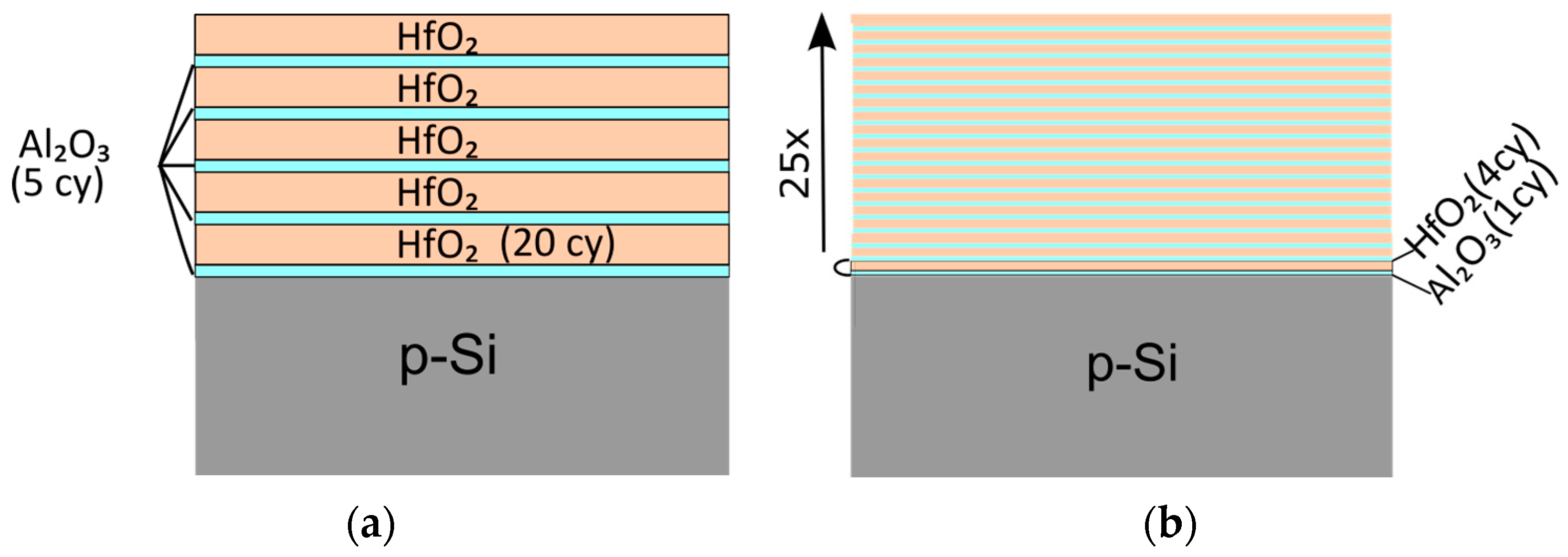
Figure 1. Schematic presentation of nanolaminated (a) and doped (b) HfO2/Al2O3 stacks.
Materials 18 05420 g001
Figure 2. The Hf 4f XPS spectra deconvoluted into two Hf 4f doublets—low BE (blue) indicating the presence of Hf suboxides and high BE (gray) one associated with stoichiometric HfO2—(a) as-deposited and (b) after RTA.
Materials 18 05420 g002
Figure 3. The O 1s core level deconvoluted into two contributions before (a) and after RTA in O2 (b).
Materials 18 05420 g003
Figure 4. The Al 2p core level spectra of pure Al2O3 film and HfO2/Al2O3 stacks before (a) and after RTA (b).
Materials 18 05420 g004
Figure 5. Valence band spectra showing the valence band maximum (VBM) values for pure HfO2 (a), nanolaminated (b), and doped (c) HfO2/Al2O3 stacks before and after RTA. The spectra are vertically shifted for visibility.
Materials 18 05420 g005
Figure 6. C-V curves of HfO2 (a) and laminated and doped HfO2/Al2O3 stacks (b) before and after RTA.
Materials 18 05420 g006
Figure 7. Schematic diagram of HfO2 bands shift upon annealing.
Materials 18 05420 g007
Table 1. Energy position of Hf 4f7/2 peak of stoichiometric and suboxide counterparts, their FWHM and the area ratio of the Hf 4f peaks of stoichiometric and substoichiometric oxide components before and after RTA.
SampleHf 4f PeakHf 4f7/2 Position, eVFWHM, eVHf 4f (Stoichiometric)/Hf 4f (Suboxide) Peak Area Ratio
As-GrownRTAAs-GrownRTAAs-GrownRTA
pure HfO2Stoichiometric17.617.41.21.21.691.92
Suboxide16.916.71.11.1
dopedStoichiometric17.517.51.01.20.551.53
Suboxide16.816.81.21.1
nanolaminatedStoichiometric17.617.41.11.10.661.5
Suboxide16.916.71.11.1
Table 2. Energy positions of the main Me-O O 1s peak and the second O 1s as well as the O 1s (main)/O 1s (2nd) area ratio before and after RTA.
SamplePeakO 1s Position, eVO 1s (Main)/O 1s (2nd) Area Ratio
As-DepositedRTAAs-DepositedRTA
pure HfO2main Me-O peak530.45530.63.94.7
second peak532.15532.3
doped main Me-O peak530.3530.23.64.9
second peak531.9532.0
nanolaminated main Me-O peak530.1530.43.56.3
second peak531.8532.3
pure Al2O3main Me-O peak531.30530.89.414.4
second peak533.00532.75
Table 3. Valence band edges of dielectric Ev(ox) and valence band offsets between dielectrics and Si for different stacks before and after RTA.
SampleValence Band Edge, Ev(ox) eVValence Band Offset ΔEv, eV
nanoalminated, as-grown3.463.22
nanolaminated, RTA3.313.07
doped, as-grown3.182.94
doped, RTA3.112.87
HfO2, as-grown3.553.31
HfO2, RTA3.323.08
Table 4. The values of fixed oxide charge, flat-band hysteresis and border traps for different stacks.
SampleTreatmentQf, cm−2Hysteresis Vfb, VQsl, cm−2
Pure HfO2as-grown3.5 × 10123.28.9 × 1012
RTA3.5 × 10120.38.8 × 1011
Nanolaminatedas-grown1.1 × 10121.23.5 × 1012
data3.9 × 10120.31.1 × 1012
Dopedas-grown1.4 × 10121.54.3 × 1012
RTA1.2 × 10120.82 × 1012
Disclaimer/Publisher’s Note: The statements, opinions and data contained in all publications are solely those of the individual author(s) and contributor(s) and not of MDPI and/or the editor(s). MDPI and/or the editor(s) disclaim responsibility for any injury to people or property resulting from any ideas, methods, instructions or products referred to in the content.