Abstract
In this study, the influence of growth temperature variation on the synthesis of MoS2 using a direct MoO2 precursor was investigated. The research showed that the growth temperature had a strong impact on the resulting morphologies. Below 650 °C, no nucleation or growth of MoS2 occurred. The optimal growth temperature for producing continuous MoS2 films without intermediate-state formation was approximately 760 °C. However, when the growth temperatures exceeded 800 °C, a transition from pure MoS2 to predominantly intermediate states was observed. This was attributed to enhanced diffusion of the precursor at higher temperatures, which reduced the local S:Mo ratio. The diffusion equation was analyzed, showing how the diffusion coefficient, diffusion length, and concentration gradients varied with temperature, consistent with the experimental observations. This study also investigated the impact of increasing the MoO2 precursor amount, resulting in the formation of multilayer MoS2 domains at the outermost growth zones. These findings provide valuable insights into the growth criteria for the effective synthesis of clean and large-area MoS2, thereby facilitating its application in semiconductors and related industries.
1. Introduction
Two-dimensional (2D) MoS2 is a popular semiconductor material with a tunable bandgap and high potential for optoelectronic applications [1,2,3]. It has been extensively explored in the literature for transistors, photodetectors, and sensors [4,5,6,7,8,9,10,11,12,13,14,15]. While mechanical exfoliation provides high-quality samples, its limited yield and random crystal sizes pose challenges for practical use. In contrast, chemical vapor deposition (CVD) offers improved scalability, yield, and film homogeneity, making it a promising method for integrating 2D MoS2 with existing technologies. However, achieving large-scale, defect-free, and cost-effective production of MoS2 remains a crucial goal. CVD-based synthesis of MoS2 films has been accomplished through sulfurization of Mo-containing precursors, including Mo [16], MoO2 [17,18,19,20,21], and MoO3 [22,23,24,25,26,27,28,29,30,31,32,33,34,35,36,37,38,39,40,41,42,43,44,45,46,47,48,49,50,51,52,53,54,55,56,57,58,59]. Among these options, the utilization of MoO3 powder as a precursor has emerged as the preferred method, owing to its ability to yield large-area single-crystal films with continuous coverage [42,43,44,45,46,47,48,49,50]. However, it is important to recognize that the use of MoO3 powder entails certain drawbacks, namely, its toxic nature (classified as a strong irritant and carcinogen based on GHS standards) and low evaporation temperature (350 °C), which pose significant health hazards and occupational risks. Consequently, it becomes imperative to identify safer alternative precursor materials to ensure that both small-scale research and large-scale production are conducted without compromising health and safety.
The synthesis of MoS2 from a conventional MoO3 precursor involves a two-step process: reduction of MoO3 to MoO2, and subsequent sulfurization of MoO2 to MoS2 [42]. However, incomplete reactions during CVD growth can lead to the formation of a MoS2−yOy phase, resulting in phase-mixing with MoS2, as frequently observed in experiments [24,26,49,60,61,62]. In a detailed study conducted by Hyun et al. [36], it was concluded that when using MoO3 as the precursor, multiple thermodynamically favorable pathways for MoS2 synthesis exist, including the sulfurization of vapor-phase MoO3, sulfurization of intermediate solid-phase MoO2, and sulfurization of vapor-phase MoO2. Among these pathways, the direct vapor-phase sulfurization (VPS) of MoO2 was found to be the most thermodynamically favorable. In the seminal experimental work of Bilgin et al. [17], an important question was raised as to whether the use of MoO3 as a precursor material is really necessary when MoO2—a more stable oxide—could be used directly, thereby avoiding the complicated reaction pathways and, hence, enabling a single-step chemical reaction: . In their work, such a direct, single-step, vapor-phase sulfurization of MoO2 was employed to successfully grow MoS2 crystals on various substrates.
It is therefore clear that a single-step VPS reaction of MoO2 should provide the best chemical pathway to synthesize MoS2 after taking into account the associated reaction simplicity, safety, and ability to greatly suppress intermediate-state formations. Despite this, there have been only a few experimental studies [17,18,21] dedicated towards evaluating the potential of directly using MoO2 as a precursor. In our recent work [21], we carried out a comprehensive study of the effect of the gas flow rate, MoO2 weight, S:Mo molar loading ratio, and growth time on MoS2 growth. A high-resolution optical stitching approach was utilized to understand and map the nature of the material grown in various growth zones. We successfully demonstrated that mm-scale continuous films of monolayer MoS2, which is free of intermediate states, could be consistently grown provided that the S:Mo loading ratio was kept above the stoichiometrically required value of 3:1 dictated by the VPS reaction of MoO2. However, the growth temperature was not varied in that study. Since temperature plays a crucial role in diffusion, it is expected to modify the concentration gradients and, hence, the local S:Mo ratio, leading to strong morphological variations across the growth substrate [21,63].
This work focuses on revealing the effects of growth temperature variation on concentration gradients, growth zone formation, MoS2 growth, and the formation of intermediate states. Our results indicate a strong dependence of temperature on the nature of the material grown. We found a cutoff temperature of 600–650 °C, below which nucleation was absent and, therefore, no growth of MoS2 was observed. We also observed that the optimal growth temperature, which minimizes intermediate-state formation and maximizes MoS2 yield, is approximately 760 °C. XPS analysis of the continuous MoS2 revealed good sample quality, with the detection of small amounts of Mo6+ states. The stoichiometric ratio of S:Mo was determined using XPS and found to be in close agreement with the expected values. XRD measurements of the CVD-grown material confirmed that the predominant material present was 2H-MoS2, with a minor contribution from MoO2.
At growth temperatures between 650 and 750 °C, while MoS2 can be successfully grown, the yield is poor due to formation of smaller growth zones in this temperature regime. On the other extreme, at growth temperatures exceeding 800 °C, we observed a drastic shift in the nature of the material grown, characterized by a transition from pure MoS2 to solely intermediate states grown across the entire substrate. These findings can be explained as a result of a significant increase in precursor diffusion at higher growth temperatures, which results in strong local modifications to the S:Mo loading ratio. By analyzing the classic diffusion equation, we can show qualitatively how the diffusion coefficient, diffusion length, and concentration gradients change as a function of temperature, and how these variations mimic our experimental findings.
The effect of increasing the amount of MoO2 precursor was also studied at growth temperatures of 700 °C and 760 °C. The findings revealed the formation of multilayer MoS2 domains in the outermost growth zones as the precursor amount was increased. At the ideal growth temperature of 760 °C, we additionally investigated the role of the substrate position. The results demonstrated the formation of the expected parabolic growth zones, with extended growth zones observed downstream, indicating enhanced diffusion in the direction of the gas flow.
A direct comparison of MoS2 growth using MoO2 and MoO3 under identical experimental conditions revealed a pronounced disparity in the morphology of the resulting materials. This distinction can be attributed to the significant differences in powder vaporization temperatures and the distinct reaction pathways leading to MoS2 formation for each precursor. These variations shed light on why the ideal growth conditions can vary significantly depending on the choice of precursor.
The combined findings of this study reveal important growth criteria under which the single-step VPS of MoO2 can be effective in growing clean and large-area MoS2. With the added advantage of being a safe and scalable approach, this work will enable further developments in the field to successfully employ MoS2 as an alternative candidate in the semiconductor and other related industries.
2. Materials and Methods
In this study, we synthesized MoS2 using the atmospheric-pressure chemical vapor deposition (APCVD) method. Our CVD system consisted of a quartz tube with a diameter of 50 mm and a single heating zone, where MoS2 growth occurred at a set growth temperature, which ranged from 600 to 850 °C in this study. Initially, a 300 nm thermal oxide Si/SiO2 wafer was cut into approximately 12 mm × 12 mm squares and cleaned by ultrasonication in acetone for 1 min, followed by an isopropyl alcohol (IPA) rinse and nitrogen gas drying. The cleaned wafer, without any additional surface treatment, was then placed face-down at the center of a small alumina boat (40 mm × 8 mm × 7 mm) loaded with MoO2 precursor (99% purity Alfa Aesar, Haverhill, MA, USA), positioned approximately 1 cm from the center of the growth substrate (see the schematic in Figure 1a).
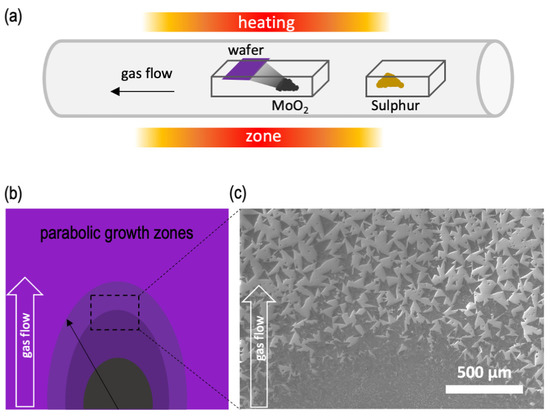
Figure 1.
(a) Schematic of the CVD setup. The alumina boat containing the MoO2 precursor and the growth substrate are positioned at the center of the heating zone, while the S precursor is placed at the edge of the growth zone. The distance between the substrate and the MoO2 source is 1 cm. (b) Schematic showing the typical zonal growth pattern of MoS2; color coding indicates varying morphology in the direction of the gas flow. (c) Example low-magnification SEM micrograph capturing the transition from continuous films to individual MoS2 domains at the outermost zones indicated (dashed box) in (b).
Separately, a different quartz boat was loaded with the required amount of sulfur powder (99.5% purity Alfa Aesar, Haverhill, MA, USA) and placed at the edge of the heating zone (details in Figure S1). The tube was then purged with Ar gas (>99.9% purity) at a flow rate of 2000 standard cubic centimeters per minute (sccm) for 5 min at room temperature. Subsequently, the flow rate was adjusted to a low value of 10 sccm, and the temperature of the heating zone was increased at a ramp rate of 15 °C/min until the desired growth temperature was reached, and it was then maintained at this level for a short time of ~1 min. At the end of the growth process, the power to the furnace was turned off, allowing the sample to naturally cool down to room temperature. Typical temperature profiles of the MoO2 and S growth zone are shown in Figure S1.
The quality and thickness of the material grown were evaluated through various techniques, including optical imaging, X-ray photoelectron spectroscopy (XPS), micro-Raman spectroscopy, photoluminescence (PL) spectroscopy, scanning electron microscopy (SEM), X-ray diffraction (XRD), and energy-dispersive X-ray spectroscopy (EDS). Optical imaging and high-resolution image stitching were conducted using a CX-40M microscope manufactured by Ningbo Sunny Instruments, Co., Ltd. (Yuyao, China). XPS measurements were performed using an Axis Supra system from Kratos Analytical Ltd., Stretford, Manchester, United Kingdom, with a monochromatic Al Kα (h = 1486.6 eV) X-ray source. Kratos ESCape software version 1.5 was used for peak assignments, and the core-level spectra were fitted with Gaussian–Lorentzian line shapes after subtracting a Shirley-type background. Stoichiometry calculations were performed by evaluating the relative areas of the relevant components, taking into consideration their system-defined relative sensitivity factors. Micro-Raman and PL spectra were acquired using a Horiba LabRAM HR Evolution confocal Raman system (Horiba Ltd., Bangkok, Thailand) with a laser excitation wavelength of 532 nm. The surface morphology and elemental maps of the grown MoS2 films were obtained using a SU8030 Field-Emission Scanning Electron Microscope (FESEM), also from Hitachi High-Tech Ltd. (Bangkok, Thailand). XRD measurements were performed using a Bruker D8 advance system (1.54 Å Cu Kα wavelength, 2θ range of 10–90°, 0.02° step size) from Bruker Scientific Instruments, Billerica, MA, USA.
3. Results and Discussions
The quantity of active Mo species available at the substrate surface plays a pivotal role in the comprehensive growth process of MoS2, particularly in terms of nucleation and subsequent domain formation. Achieving a uniform distribution of gaseous-phase S is typically accomplished by maintaining a substantial distance between the S source and the growth substrate. In contrast, the Mo-containing source is typically positioned in close proximity to the growth substrate in order to ensure successful MoS2 growth. Consequently, this leads to the formation of a distinct gradient-like concentration distribution of the MoS2 nucleation sites on the substrate surface. This concentration gradient acts as a fundamental framework for dictating the final growth pattern, which typically presents as parabolic growth zones with varying morphologies, as illustrated in the schematic shown in Figure 1b. Figure 1c shows an SEM micrograph illustrating the transition from continuous films to individual domains in the outermost growth zones.
Numerical simulations, employing finite element modeling techniques conducted by R. A. Vila et al. [63], elucidated the behavior of the concentration gradient on the substrate surface as a function of the distance from the Mo source. The simulations revealed a gradual decrease in the concentration gradient, which is expected due to mixing and diffusion of the precursor in the ambient gas as it is pushed downstream by the argon carrier gas, corroborating the experimental observations of characteristic parabolic growth zones [25,30,37,46,50]. Moreover, the existence of such a concentration gradient instigates variations in the local Mo:S ratio along the length of the growth substrate, thereby augmenting the probability of diverse morphological evolutions [63], oxysulfide formations [34,37,49,60,61,62], and modifications in MoS2 domain shapes [25]. These findings underscore the significance of understanding and controlling the concentration gradient of active Mo species during MoS2 growth. The precise manipulation of this gradient can potentially be exploited to engineer and tailor the properties and characteristics of MoS2 nanostructures, thereby facilitating advancements in various technological applications.
3.1. Effect of Growth Temperature on MoS2 Growth
3.1.1. Temperature Dependence
We began by first analyzing the MoS2 growth process at several different temperatures, ranging from 600 °C to 850 °C. The growth results are summarized in Figure 2 and Figure 3. In general, we consistently found no growth on the substrate when the growth temperature fell below 600 °C. This indicates that MoO2 exhibits a comparatively lower vaporization propensity than MoO3, which is well documented to vaporize even at temperatures as low as 350 °C. As the temperature is raised beyond 600 °C, MoS2 growth begins. Importantly, a systematic increase in growth zones, as shown in the schematics of Figure 2a and Figure 3a, was observed in the growth results.
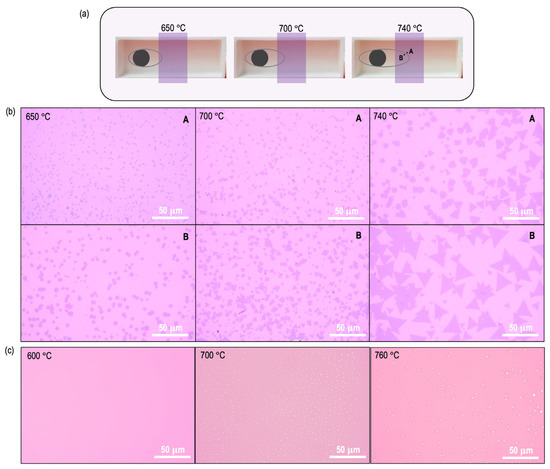
Figure 2.
(a) Schematic depicting the increase in growth zones as a function of growth temperature. (b) Representative high-resolution optical images captured at indicated locations A and B in (a) for growth temperatures of 650 °C, 700 °C, and 740 °C. Locations A and B capture growth variations across the boundary of the outermost growth zone. (c) Optical images capturing nucleation density and seed size variation as the growth temperature is increased from 600 °C to 800 °C. Sulfur precursors were eliminated in this experiment. False color is used to make the individual seed size more visible.
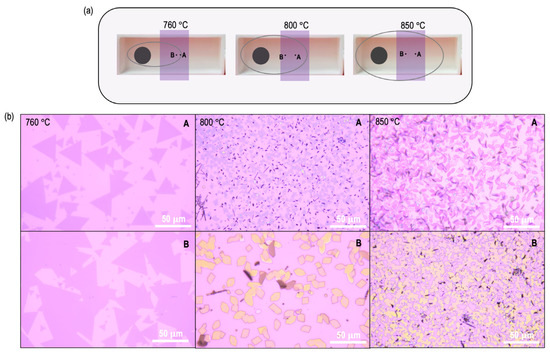
Figure 3.
(a) Schematic depicting the dramatic increase in growth zones (grey oval) as the growth temperature is increased from 760 °C to 800 °C. (b) High-resolution optical images obtained at approximate locations around points A and B indicated in (a), for growth temperatures of 760 °C, 800 °C, and 850 °C, capturing the morphological evolution across these temperatures. Growth is typically absent below 650 °C. Optical images corresponding to growth results at 800 °C and 850 °C clearly indicate a shift to intermediate-state formation, while at 760 °C, ideal MoS2 domain size and density are obtained.
Optical images captured for two closely spaced points (indicated in Figure 2a) that lie inside and outside the outermost growth zone are shown in Figure 2b for the temperatures of 650 °C, 700 °C, and 740 °C. It is clear from these images that at the lower temperatures of 650 °C and 700 °C, the grown MoS2 domain sizes are small, while the density is large. As the temperature increases to 740 °C, a clear deviation from this trend is observed, with an increase in domain size and a reduction in nucleation density. Optical images for the 600 °C condition, where no MoS2 growth occurs, were omitted from these results.
To delve deeper into the findings shown in Figure 2b, we investigated the impact of growth temperature on nucleation density and size, while deliberately omitting sulfur during the synthesis process. Figure 2c summarizes the results obtained at temperatures of 600 °C, 700 °C, and 760 °C. At 600 °C, it is clear that no nucleation sites exist. At 700 °C, the nucleation density appears to be large, while the individual seed sizes are very small. As the growth temperature is increased to 760 °C, two effects can be seen: a decrease in nucleation density, and a visible increase in seed size. These findings are consistent with the MoS2 growth results obtained at 760 °C (see Figure 3b), where we obtained large domain sizes, and the low nucleation density allows for the formation of continuous films with large grain-boundary separations (see Figure S2).
For the interested reader, a detailed investigation of grain-boundary separations at this temperature can be found in our previous study [21]. Shifting our attention now to the growth results obtained at 800 °C and 850 °C (Figure 3b), a stark deviation in the growth results is observed. At both of these temperatures, the central regions of the growth substrates are predominantly covered with intermediate states, and little-to-no MoS2 is grown here. Notably, this effect is much stronger at the highest temperature investigated here (850 °C).
To understand the correlation between the formation of intermediate states at temperatures above 800 °C and the absence of them at lower temperatures, we turned to a detailed analysis of the growth results obtained at 760 °C and 800 °C. To facilitate comprehensive visualization, we employed a high-resolution optical stitching approach, enabling the mapping of a centimeter-scale image encompassing the entire growth substrate. It is evident from the growth results obtained at 760 °C (see Figure 4) that the typical parabolic growth zones can be clearly observed.
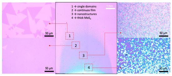
Figure 4.
Detailed analysis of the growth results obtained at 760 °C. The center image corresponds to the high-resolution optically stitched image displaying the material grown on the entire substrate. Typical growth zones were obtained, similar to the schematic shown in Figure 1. The regions closest to the substrate edge are dominated by thick but pure MoS2 (bulk and nanostructures), while the morphology evolves to continuous MoS2 and individual triangular domains in the downstream regions, as indicated by high-magnification optical images displaying the morphology of materials grown in the regions marked 1–4. Detailed Raman line mapping of similar growth conditions may be obtained from our prior study [21].
The zones closest to the substrate edge are dominated by thick MoS2 and nanostructures. This is followed by a zone of continuous mm-scale film and, finally, the outermost zone consisting of individual MoS2 domains. Representative high-magnification optical images corresponding to regions 1–4 marked in the growth zones can be seen in Figure 4. The morphological variation between the various zones stems from the gradual change in the local S:Mo ratio along the gas flow direction [63].
X-ray photoelectron spectroscopy (XPS) was employed to analyze the chemical state of monolayer MoS2 films. The wide-spectrum scan shown in Figure 5a confirms the presence of Mo and S signals.
Figure 5.
XPS spectra obtained for continuous MoS2 (region 2 of Figure 4): (a) Wide-spectrum scans revealing the presence of Mo and S signals. (b) Mo-3d and S2s core-level scans. (c) S-2p core-level scans.
Additional peaks corresponding to oxygen (-O) and silicon (Si) were observed, likely originating from the SiO2/Si substrate. The C-1s peak stems from surface contamination. Figure 5b,c display high-resolution scans focusing on the Mo-3d and S-2p core-level spectra, respectively. The Mo-3d spectrum shows both the Mo-3d and S-2s core-level signals, which can be fitted with three Mo-3d doublets and one singlet peak (S-2s), respectively. The most intense Mo4+ doublet state (black trace) consists of two distinct peaks identified at 230.0 (3d5/2) and 233.12 eV (3d3/2), with a spin–orbit splitting (Δ) of approximately 3.12 eV. These peak positions closely match those reported for the Mo4+ oxidation state [64]. The absorption shoulder seen at 227.17 eV corresponds to the binding energy of the S-2s electron. The doublet peak located at 231.77 eV (red trace) stems from defect Mo4+ (d-Mo4+), corresponding to Mo atoms close to sulfur vacancies [65,66,67]. Finally, the doublet peak at the binding energy of 233.12 eV is due to the Mo6+ of Mo-O bonds [68,69,70] and can seemingly arise from various sources. It has been attributed to the presence of unreacted precursors [61,71], which are known to be a common source of contamination in CVD-grown MoS2. It has also been suggested that the Mo6+ states could be associated with surface oxidation from air exposure and cycling [72,73], and that these peaks are largely suppressed upon etching of samples for 10 s [73]. A further possibility is that the Mo6+ states originate from the formation of interfacial Mo-O bonds at the MoS2–SiO2 interface [74]. It is also important to consider the possibility of oxidation of MoO2 to MoO3 in the context of this study.
Examination of the sulfur chemical environment (Figure 5c) reveals a single doublet that can be resolved into the S 2p3/2 and 2p1/2 levels at 162.8 and 164.0 eV (Δ = 1.2 eV), respectively, indicating the presence of S2 states in MoS2 [65,66,75,76]. The absence of a higher binding energy doublet in the S-2p spectrum, the presence of a single S2s peak in the Mo-3d spectrum, and the very low d-Mo4+ contribution together indicate that effective sulfurization of the MoS2 has occurred [77].
The stoichiometry of the formed MoS2 material can be estimated by taking the ratios of the calculated atomic concentrations of the S-2p and Mo-3d components (see Table S1). This yields S:Mo values of ~1.7 and ~1.82, with and without including the d-Mo4+ contribution, respectively. These values are close to the value of ~1.86 reported for mechanically exfoliated MoS2 [58] and the statistically obtained average value of ~1.89 for MoS2 thin films reported in the literature [78]. Alternately, as outlined in the systematic study by Baker et al. [79], the MoS2 stoichiometry can also be determined to an accuracy of by measuring the distance between the S 2p3/2 and Mo 3d5/2 peaks. As shown in Table S1, we obtained a distance of 67.16 eV, which indicates a stoichiometric value of ~1.98 [67,79] for our sample. The contrasting methods make it challenging to use XPS to estimate the actual material’s stoichiometry, despite it being the most widely used composition analysis technique. Additionally, EDS mapping (Figure S3) was also performed for the continuous MoS2 and the bulk products. While the elemental maps of S and Mo confirm the presence of MoS2, the calculation of stoichiometry leads to erroneous results owing to the weak signal detection and the overlapping S and Mo energies [80,81], which is particularly problematic for the case of MoS2. Hence, this technique is not recommended for the reliable estimation of stoichiometry in monolayer and very-thin films of this material.
XRD analysis was conducted to gain further insights into the composition and phase of the materials grown on the substrate (refer to Figure S4 for details). The analysis confirmed the predominance of a pure 2H-MoS2 phase, aligning with findings from thin-film MoS2 grown using CVD [82]. Furthermore, the 2H MoS2 phase purity can be independently confirmed from the results of XRD, XPS (Figure 5), and Raman spectroscopy (see Figure 6), as they exhibit no related signals corresponding to the 1T-MoS2 phase [72,83,84]. XRD additionally revealed the presence of trace amounts of the precursor MoO2. We believe these to have arisen from unreacted precursors left behind upon cessation of CVD growth, as materials freeze at this stage and cannot be driven to complete reaction [85]. Overall, these observations are in reasonable agreement with the XPS findings.
Figure 6.
Detailed analysis of the growth results obtained at 800 °C: (a) High-resolution optically stitched image displaying the material grown on the entire substrate. The central regions of the substrate are dominated by intermediate states, while clean and continuous MoS2 grows towards the substrate edges and the downstream-most location of the substrate. The empty no-growth regions correspond to the area of the substrate overlapping the rim of the alumina crucible. (b) High-magnification optical images displaying the morphology of material grown in the regions labeled 1–6 in (a). (c,d) Raman traces obtained over a wide wavenumber range to highlight the difference in morphology at the central region of the wafer (predominantly MoOS2) vs. the edges (solely MoS2).
Shifting our focus to the growth results achieved at 800 °C, it is evident from the optically mapped image in Figure 6a that a significant departure from the conventional parabolic growth zone pattern (as shown in Figure 4) has occurred.
The results reveal an interesting picture. Here, the majority of the middle region contains little-to-no visible growth of MoS2 and is instead largely dominated by intermediate states. Interestingly, continuous films of MoS2 now tend to grow on the left and right sides of the wafer. It must be noted that these growth regions lie exactly outside the rim of the alumina boat, representing the overhanging part of the substrate. Additionally, as indicated in Figure 6a, a region of continuous MoS2 is also found in the downstream-most location of the substrate. In the lateral direction and towards the end of the zone containing intermediate states, we can observe the formation of truncated MoS2 domains. Representative optical images capturing the various morphologies corresponding to the locations marked in Figure 6a are shown in Figure 6b. It can be seen from these images that the varying morphologies are closely related to their growth location on the substrate.
The results of wide-wavenumber Raman point analysis conducted in regions 1 and 3 are shown in Figure 6c,d, respectively. In Figure 6c, the two dominant Raman vibration modes that are characteristic of MoS2 can be seen. The E12g mode, corresponding to the in-plane vibration of S and Mo atoms, can be seen at a wavenumber of approximately 381.5 cm−1, while the A1g mode, corresponding to the out-of-plane vibrations of S atoms, can be seen at about 400 cm−1. The resulting frequency difference () between the two modes is therefore 18.5 cm−1, confirming the monolayer nature of the grown MoS2 [86,87]. In contrast, as shown in Figure 6d, the Raman trace obtained from region 3 revealed the grown material to be intermediate MoOS2. While we have not pursued extensive line or area Raman mapping, simple optical inspection is usually sufficient to identify intermediate states that are known to have very distinct morphologies (rectangular domains) when compared to MoS2 and can therefore be easily identified on a substrate.
It must be highlighted that, in contrast to our previous study [21], where we found that intermediate-state formation was largely quenched as long as the global S:Mo loading ratio was kept below the stoichiometrically required value of 3:1 required by the single-step VPS of MoO2, the appearance of intermediate states at higher temperatures in the present study, in spite of the global S:Mo loading ratio (20:1) being maintained well above the required 3:1 value, suggests a dramatic shift in the locally available S:Mo molar loading ratio at the higher growth temperatures. In order to explain this, let us consider the overhanging regions of the substrate where continuous films of MoS2 are formed. Here, the local S:Mo ratio should be large enough, and this may be possible due to the low availability of the Mo precursor at these locations. This is logical, as these locations are situated at the greatest lateral distance from the MoO2 source. On the other hand, driven by the high CVD temperature, the local Mo precursor available in the middle region of the substrate is substantially large in comparison, and this inevitably drives the local S:Mo ratio to very low values, thereby facilitating the formation of predominantly intermediate states. The formation of truncated domains in the regions indicated in Figure 6a suggests that the local S:Mo available here is just slightly below the stoichiometric requirement to fully form MoS2. This therefore indicates a decrease in the Mo concentration along the lateral direction of the growth zones. Along the direction of the gas flow, however, the decrease in the Mo concentration is more gradual, thereby leading to the slow morphological evolution seen in the captured images at locations 3–6 in Figure 6a. Here, one can see how the morphology evolves from predominantly intermediate MoOS2 growth at location 3 to a reduction in their sizes and the emergence of nanostructures at location 4. Continuing on to location 5, nanostructures dominate the growth, and further investigation of SEM images (Figure S5) reveals the formation of vertically-oriented structures in the mix. Finally, at location 6, small domains of MoS2 are predominant. As noted already, as we proceed further to the downstream-most location of the substrate, the morphology transitions to continuous films of MoS2, which simply means that the local S:Mo has increased enough to exit the regime of intermediate-state formation and enter the regime where the stoichiometric value is closer to or above 3:1.
The drastic differences in the growth outcomes at 760 °C and 800 °C may be further explained as a result of a dramatic increase in the diffusion behavior of the MoO2 precursor as the growth temperature is raised to and beyond 800 °C. Experimentally, this can be seen in the photograph shown in Figure 7a.
Figure 7.
(a) Photograph of the alumina boat taken after growth was completed at the indicated growth temperatures. A dramatic change in precursor diffusion was noted at temperatures at and above 800 °C. Qualitative plots of the (b) diffusion coefficient and (c) diffusion length as a function of temperature at molecular sizes (a values) close to the expected value of MoO2 molecules. (d) Concentration profile vs. position from the precursor source, plotted using Equation (1), at a few indicated temperatures. (e) Concentration as a function of temperature at a few arbitrarily chosen residence time values.
Here, we captured snapshots of the boat’s condition after the completion of the CVD growth process at each of the indicated temperatures. Clearly, the expansion of the black-shaded regions (which may be visualized as the region of precursor diffusion or the region where a concentration gradient exists) varies as the temperature is increased, with the effect seen to be pronounced at the highest temperatures.
In general, the diffusion of MoO2 vapor from the source to the substrate can be quantified by using a common solution to the diffusion equation [88]:
where t is the residence time of gases, D is the diffusion constant, and and are the concentrations of the gaseous species at the source and at a distance away from the source, respectively. The unit of the diffusion constant is length2/second and is a function of temperature (T), pressure (P), and the radius of the precursor molecule (a). A rough estimate of D for a gas composed of hard spheres of equal size and mass is given as follows [88]:
where k is the Boltzmann constant. From Equation (2), if we assume a constant pressure of 1 atm (APCVD), it is evident that the diffusion constant increases as T increases. Another important parameter that relates to the diffusion constant and time is the diffusion length, Ld = 2(Dt)1/2, and is understood as the characteristic length scale that obeys the diffusion equation. From this relation, one expects the diffusion length to also increase with temperature. These expected variations are evident in the plots shown in Figure 7b,c, where both D and Ld values are plotted against temperature, respectively, within the range of values corresponding to the expected molecule size, a, of MoO2. The mass of the particles is calculated using knowledge of the molar mass (127.9 g/mol) of MoO2.
Using Equation (1), one can plot the variation in the concentration of available precursors at a distance x from the source. Assuming a short residence time (t) of 0.1 s and n (x = 0) = 1 gives us the concentration variation shown in Figure 7d, for several different temperatures, ranging from 400 to 1000 K. Two main conclusions can be drawn from the trends observed here: First, it is clear that the concentration of reacting MoO2 species at any given distance from the substrate increases with temperature. From the photograph shown in Figure 7a, we can note that the substrate position was fixed in all of our experiments at ~1 cm from the MoO2 source. The results of Figure 7d therefore suggest a significant reduction in the local S:Mo ratio as the growth temperature is raised, which explains the experimental observations of the strong formation of intermediate states at the highest temperatures of 800 °C and 850 °C. Second, it can also be seen in Figure 7d that, at higher temperatures, the concentration gradients can be strong and can extend along longer portions of the substrate. For example, from the 1000 K trace (pink), the concentration drops by nearly 70% across the length of the substrate. This explains the observation of larger growth zones and the morphologies transitioning from largely intermediate states in the bulk of the substrate to continuous films at the downstream-most edge of the substrate (see Figure 6a). These trends are further substantiated by the fact that at the highest growth temperature of 850 °C we found most of the growth substrate to be filled with nanostructures and intermediate states, while the overhanging portions of the wafer showed growth of truncated domains (Figure S6). While we did not perform detailed optical mapping of this case, the dramatic increase in the MoO2 precursor concentration and, hence, the low local S:Mo ratio, can be seen from the differences already noted from Figure 3b, as well as from the photograph shown in Figure 7a.
A note of caution is necessary regarding the variations presented in Figure 7b,c, as they are qualitative in nature and were plotted using a relatively short residence time to approximately mimic the experimental observations. A more robust quantitative analysis is not possible using Equation (1), since the powder vaporization of MoO2 occurs at much higher temperatures. We expect that more refined numerical simulations employing finite element analysis may be required for an accurate description of the actual diffusion dynamics. Having said that, it can be noted in Figure 7d, where we plotted concentration (at x = 1.5 cm) vs. temperature at a few different residence time values, that as the temperature increases the concentration increases rapidly at first, before saturating at higher values of T. This behavior is consistent with our experimental results, where we can see rapid changes in morphology within a short growth-temperature window.
A further point can be made as relates to the precursor type. For instance, considering the case of MoO2 vs. MoO3, while the diffusion equation would yield qualitative curves similar to those shown in Figure 7 for MoO3, the actual diffusion behavior could be vastly different for the two precursors when considering that the powder vaporization of these precursors occurs at very different temperatures. Consequently, this will result in completely different concentration profiles across the substrate and, hence, different S:Mo precursor ratios available for growth. The difference in reaction pathways between the two precursors can also be viewed as important, because the VPS of MoO3 to MoS2 is a multistep process, as opposed to the single-step VPS of MoO2. Experimental validation of these assumptions can be found in Figure S7 of the Supplementary Materials, where we show how, under the exact same experimental conditions, the morphology of the material grown on the substrate when using MoO3 is in striking contrast to that obtained when using MoO2 precursors. These findings therefore suggest that the experimental parameters necessary for obtaining ideal MoS2 growth could vary vastly depending on the choice of Mo precursor source.
3.1.2. Effect of Varying MoO2 Precursor Amount/Formation of Multilayers
In this section, we focus on the lower temperatures, where intermediate states are absent, and we explore the effect of changing the MoO2 precursor quantity. The results obtained at growth temperatures of 700 °C and 760 °C are shown in Figure 8a, from which it is evident that while the increase in the MoO2 quantity results in larger MoS2 domain sizes, it also initiates the formation of multilayers.
Figure 8.
Effect of varying the MoO2 precursor quantity: (a) Optical images capturing the formation of multilayer MoS2 as the MoO2 precursor quantity is increased from 2 mg to 5 mg to 10 mg. The upper and lower panels correspond to the growth results obtained at 700 °C and 760 °C, respectively. (b) SEM image showing multilayer formation and seeds. (c) Photoluminescence (PL) trace showing the characteristic A and B excitonic peaks for single-layer and multilayer/bulk MoS2. (d) Wide-wavenumber Raman spectra showing the characteristic E12g and A1g peaks of MoS2 and the absence of low-wavenumber peaks corresponding to intermediate states. Inset shows the calculated peak difference values.
The effect is pronounced at the highest MoO2 quantity of ~10 mg, as evident from the multilayer formation even at the lower temperature of 700 °C, where the domain sizes are small. These findings are consistent with Equation (1), where it can be seen that the concentration increases proportionally to the precursor concentration set at x = 0. Upon further inspection of the optical images shown in Figure 8a, it can be seen that the additional layers grow from the center of the MoS2 flake, which results from the increased MoO2 concentration. The presence of seeds and the grown multilayers can be seen more clearly in the SEM micrographs shown in Figure 8b.
In Figure 8c, we show an example photoluminescence (PL) spectrum of the monolayer and multilayer domains. The presence of the characteristic A and B direct excitonic transitions at approximately 1.81 and 1.95 eV, respectively, in the monolayer MoS2 domain, along with the notable intensity of the A peak, serves to indicate both the monolayer nature and the excellent crystalline quality of the grown MoS2 [2,17]. Conversely, when examining spectra obtained from the multilayer domain, a decrease in the photoluminescence (PL) intensity is observed, accompanied by a slight redshift in the excitonic transitions. These results are consistent with the observed characteristics exhibited by both CVD-grown and exfoliated MoS2 layers, as reported in previous studies [89,90,91]. The main panel of Figure 8d shows Raman spectra corresponding to the monolayer and multilayer MoS2 domains, obtained over a wide wavenumber range. The two dominant Raman vibration modes that are characteristic of MoS2 can be seen here, and the absence of any intermediate-state formation is proven by the absence of additional peaks in the low-wavenumber region. The E12g mode, corresponding to the in-plane vibration of S and Mo atoms, is seen at a wavenumber of approximately 385.4 cm−1, while the A1g mode, corresponding to the out-of-plane vibrations of S atoms, is seen at about 402 cm−1 (see the inset in Figure 8d). The resulting frequency difference () between the two modes is therefore 16.7 cm−1, confirming the monolayer nature of the MoS2 domain [86,87]. In agreement with the literature [86], the peak difference obtained for the multilayer/bulk MoS2 was found to be ~26 cm−1.
3.2. Role of Substrate Position
We can obtain further insights on the diffusion of precursors by studying the role of the substrate position. Due to the role of gas flow driving the reactants, it is expected that a larger diffusion zone will be formed downstream from the precursor location than in the upstream direction. The schematic shown in Figure 9a illustrates this effect.
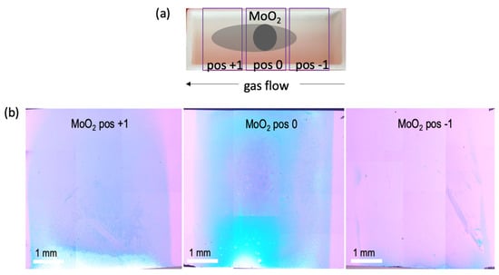
Figure 9.
(a) Schematic setup used to study the effect of varying substrate position with respect to the Mo precursor used. (b) Optical stitched images capturing the formation of MoS2 growth zones for positions +1 cm, 0 cm, and −1 cm from the MoO2 source.
As a result, the variation in the substrate position should result in growth zones following this pattern. This is evident in Figure 9b, where we show the growth results obtained through optical image stitching at a growth temperature of 760 °C and at three different substrate positions, labeled −1 cm, 0 cm, and +1 cm. The zero position corresponds to the situation where the substrate is placed exactly over the precursor location. At this position, as expected, the majority of the substrate is covered with thick MoS2 material, which corresponds to the white- and blue-colored regions on the substrate. At the position +1 cm, the classic parabolic zones emerge, with each zone exhibiting varying morphological characteristics.
Based on the above observations, it is perceivable that increasing the sample height in the experiment should lead to growth behavior mimicking that obtained when changing the horizontal position of the substrate. By applying the diffusion equation in the vertical direction, one should expect a systematic reduction in the Mo precursor concentration with sample height, and this should, in principle, allow for the growth of more homogenous MoS2 thin films at an experimentally determined optimal height. While the specific experiments to reveal the expected growth–height dependence were not conducted in this study, the insights obtained may help improve our understanding of the growth process. We should note that under the experimental conditions used in the current study, diffusion-limited growth predominated, as evidenced by the distinct parabolic zone growth pattern. To obtain homogenous and continuous MoS2 films that are large-scale (or even wafer-scale), it would be necessary to modify the experimental parameters such that growth can happen outside the diffusion-limited regime. As indicated in the literature, several strategies may be employed, including the reduction in Mo precursor quantity [55], space confinement [56], increasing the substrate–source gap height [26], using barriers [49], or employing a multisource tube furnace that allows for more uniform Mo precursor concentration available at the growth substrate [48]. In a previously published work [21], we have also shown how changing the MoO2 precursor distribution on the boat can dramatically alter the zonal pattern and lead to better substrate coverage.
Having said that, in order to gain a comprehensive understanding of the diffusion processes involved in the CVD growth of MoS2 using MoO2, further investigation is needed, particularly in the context of low-pressure chemical vapor deposition (LPCVD). Equation (2) clearly suggests that the diffusion coefficient varies much more strongly with pressure than with temperature. Reducing the pressure to 1 Torr, for instance, can dramatically increase the diffusion length and, hence, drive the reaction out of the diffusion-limited regime. Additionally, the influence of the gas flow rate and sulfur precursor quantity on diffusion and the formation of growth zones should be carefully considered. Our preliminary findings suggest a potential dependency, as evidenced by the varying extent of the observed parabolic growth zones in relation to these parameters. However, the present results are inconclusive, highlighting the necessity for more extensive experiments. These forthcoming investigations will be part of our future work, aiming to provide deeper insights into these aspects of diffusion phenomena.
4. Conclusions
We conducted a detailed study of the effect of growth temperature in the single-step VPS of MoS2 using direct MoO2 precursors. In general, our experiments revealed the diffusion of MoO2 to be a strong function of temperature, as evidenced by two key findings: the dramatic enlargement of growth zones, and the strong morphological changes observed across the growth substrate. By varying the temperature in a wide range of 600–850 °C, we were able to identify important growth criteria for the formation of large-scale MoS2. For the given set of experimental conditions investigated in this study, we found that at temperatures below 650 °C, no MoS2 growth occurred, which we attributed to the high vaporization temperature of MoO2 and, hence, the absence of nucleation. Between temperatures of 650 and 700 °C, growth commenced, but the yield of MoS2 was small due to the small growth zones. At 760 °C, expanded growth zones allowed us to see the morphological change from thick MoS2 to nanostructures at the upstream location of the substrate, and to mm-scale continuous monolayer MoS2 and individual domains in the downstream regions. At the downstream locations, the domain growth was characterized by lower density and large sizes, which coalesced to form continuous monolayer MoS2 with large grain-boundary separations. Increasing the MoO2 precursor quantity revealed the formation of multilayer MoS2 in the outermost growth zones. The observed morphological evolutions from thick MoS2 to nanostructures to MoS2 can be understood to be a result of the increasing local S:Mo ratio along this direction.
Raising the growth temperature to 800 °C revealed dramatic changes in the morphology, with intermediate states dominating the CVD growth, and the various morphologies obtained could be associated with the expected local S:Mo variations in those regions. By performing a qualitative analysis of the diffusion equation, we showed how the diffusion coefficient and the concentration gradient are strong functions of temperature, and how they can be utilized to interpret the experimental observations. Finally, we also studied the dependence of substrate-to-MoO2-precursor distance and found the growth zone formation to be consistent with expectations. When directly comparing the growth of MoS2 using MoO2 and MoO3 precursors, we observed significant differences in the morphology of the grown materials. We attributed these findings to the differences in diffusion behavior and vaporization temperatures, in addition to significant differences in the reaction pathways associated with these precursors.
In conclusion, although additional research is necessary to gain a complete understanding of the characteristics and applications of MoO2 precursors for producing pristine and large-scale MoS2, we firmly believe that the findings presented in this study will provide a foundation for the successful adoption of MoO2 as a precursor in the commercial growth of MoS2, ensuring both high quality and safety standards.
Supplementary Materials
The following supporting information can be downloaded at: https://www.mdpi.com/article/10.3390/ma16134817/s1, Figure S1: Growth temperature profiles; Figure S2: MoS2 domain size and grain-boundary separation; Figure S3: Elemental Mapping results; Figure S4: XRD results; Figure S5: Morphology evolutions at 800 °C; Figure S6: Morphology evolutions at 850 °C; Figure S7: Precursor comparison; Table S1: XPS Quantification- Determination of Stoichiometry.
Author Contributions
Conceptualization, R.S. and H.R.; methodology, H.R.; validation, H.R. and R.S.; formal analysis, H.R., T.C. and W.B.-a.; investigation, T.C. and W.B.-a.; resources, R.S.; data curation, H.R. and T.C.; writing—original draft preparation, H.R.; writing—review and editing, R.S. and H.R.; visualization, H.R.; supervision, H.R.; project administration, R.S.; funding acquisition, R.S. and H.R. All authors have read and agreed to the published version of the manuscript.
Funding
This project was funded by the National Research Council of Thailand (NRCT), contract number N42A650226. The Research by King Mongkut’s Institute of Technology Ladkrabang (KMITL) received funding support from the NSRF (FRB660065/0258-RE-KRIS/FF66/14 and FRB660065/0258-RE-KRIS/FF66/13). H.R. acknowledges support from King Mongkut’s Institute of Technology Ladkrabang (grant no KREF046302).
Institutional Review Board Statement
Not applicable.
Informed Consent Statement
Not applicable.
Data Availability Statement
The data presented in this study are available upon request from the corresponding author. The data are not publicly available due to legal/ethical reasons.
Conflicts of Interest
The authors declare no conflict of interest. The funders had no role in the design of the study; in the collection, analyses, or interpretation of data; in the writing of the manuscript; or in the decision to publish the results.
References
- Splendiani, A.; Sun, L.; Zhang, Y.; Li, T.; Kim, J.; Chim, C.Y.; Galli, G.; Wang, F. Emerging photoluminescence in monolayer MoS2. Nano Lett. 2010, 10, 1271–1275. [Google Scholar] [CrossRef]
- Mak, K.F.; Lee, C.; Hone, J.; Shan, J.; Heinz, T.F. Atomically thin MoS2: A new direct-gap semiconductor. Phys. Rev. Lett. 2010, 105, 2–5. [Google Scholar] [CrossRef]
- Radisavljevic, B.; Radenovic, A.; Brivio, J.; Giacometti, V.; Kis, A. Single-layer MoS2 transistors. Nat. Nanotechnol. 2011, 6, 147–150. [Google Scholar] [CrossRef] [PubMed]
- Yin, Z.; Li, H.; Li, H.; Jiang, L.; Shi, Y.; Sun, Y.; Lu, G.; Zhang, Q.; Chen, X.; Zhang, H. Single-layer MoS2 phototransistors. ACS Nano 2012, 6, 74–80. [Google Scholar] [CrossRef]
- Late, D.J.; Huang, Y.K.; Liu, B.; Acharya, J.; Shirodkar, S.N.; Luo, J.; Yan, A.; Charles, D.; Waghmare, U.V.; Dravid, V.P.; et al. Sensing behavior of atomically thin-layered MoS2 transistors. ACS Nano 2013, 7, 4879–4891. [Google Scholar] [CrossRef]
- Lopez-Sanchez, O.; Lembke, D.; Kayci, M.; Radenovic, A.; Kis, A. Ultrasensitive photodetectors based on monolayer MoS2. Nat. Nanotechnol. 2013, 8, 497–501. [Google Scholar] [CrossRef]
- Mak, K.F.; He, K.; Lee, C.; Lee, G.H.; Hone, J.; Heinz, T.F.; Shan, J. Tightly bound trions in monolayer MoS2. Nat. Mater. 2013, 12, 207–211. [Google Scholar] [CrossRef]
- Perkins, F.K.; Friedman, A.L.; Cobas, E.; Campbell, P.M.; Jernigan, G.G.; Jonker, B.T. Chemical vapor sensing with monolayer MoS2. Nano Lett. 2013, 13, 668–673. [Google Scholar] [CrossRef]
- Salehzadeh, O.; Tran, N.H.; Liu, X.; Shih, I.; Mi, Z. Exciton kinetics, quantum efficiency, and efficiency droop of monolayer MoS2 light-emitting devices. Nano Lett. 2014, 14, 4125. [Google Scholar] [CrossRef]
- Wu, W.; Wang, L.; Li, Y.; Zhang, F.; Lin, L.; Niu, S.; Chenet, D.; Zhang, X.; Hao, Y.; Heinz, T.F.; et al. Piezoelectricity of single-atomic-layer MoS2 for energy conversion and piezotronics. Nature 2014, 514, 470–474. [Google Scholar] [CrossRef]
- Xue, F.; Chen, L.; Wang, L.; Pang, Y.; Chen, J.; Zhang, C.; Wang, Z.L. MoS2 tribotronic transistor for smart tactile switch. Adv. Funct. Mater. 2016, 26, 2104–2109. [Google Scholar] [CrossRef]
- He, G.; Ghosh, K.; Singisetti, U.; Ramamoorthy, H.; Somphonsane, R.; Bohra, G.; Matsunaga, M.; Higuchi, A.; Aoki, N.; Najmaei, S.; et al. Conduction mechanisms in CVD-Grown monolayer MoS2 transistors: From variable-range hopping to velocity saturation. Nano Lett. 2015, 15, 5052–5058. [Google Scholar] [CrossRef] [PubMed]
- Park, M.; Park, Y.J.; Chen, X.; Park, Y.K.; Kim, M.S.; Ahn, J.H. MoS2-Based tactile sensor for electronic skin applications. Adv. Mater. 2016, 28, 2556–2562. [Google Scholar] [CrossRef] [PubMed]
- Nikam, R.D.; Sonawane, P.A.; Sankar, R.; Chen, Y.T. Epitaxial growth of vertically stacked p-MoS2/n-MoS2 heterostructures by chemical vapor deposition for light emitting devices. Nano Energy 2017, 32, 454–462. [Google Scholar] [CrossRef]
- Singh, E.; Singh, P.; Kim, K.S.; Yeom, G.Y.; Nalwa, H.S. Flexible Molybdenum Disulfide (MoS2) Atomic Layers for Wearable Electronics and Optoelectronics. ACS Appl. Mater. Interfaces 2019, 11, 11061–11105. [Google Scholar] [CrossRef]
- Zhan, Y.; Liu, Z.; Najmaei, S.; Ajayan, P.M.; Lou, J. Large-area vapor-phase growth and characterization of MoS2 atomic layers on a SiO2 substrate. Small 2012, 8, 966–971. [Google Scholar] [CrossRef]
- Bilgin, I.; Liu, F.; Vargas, A.; Winchester, A.; Man, M.K.L.; Upmanyu, M.; Dani, K.M.; Gupta, G.; Talapatra, S.; Mohite, A.D.; et al. Chemical vapor deposition synthesized atomically thin molybdenum disulfide with optoelectronic-grade crystalline quality. ACS Nano 2015, 9, 8822–8832. [Google Scholar] [CrossRef]
- Xie, Y.; Wang, Z.; Zhan, Y.; Zhang, P.; Wu, R.; Jiang, T.; Wu, S.; Wang, H.; Zhao, Y.; Nan, T.; et al. Controllable growth of monolayer MoS2 by chemical vapor deposition via close MoO2 precursor for electrical and optical applications. Nanotechnology 2017, 28, 2–3. [Google Scholar] [CrossRef]
- Zhu, D.; Shu, H.; Jiang, F.; Lv, D.; Asokan, V.; Omar, O.; Yuan, J.; Zhang, Z.; Jin, C. Capture the growth kinetics of CVD growth of two-dimensional MoS2. Npj 2D Mater. Appl. 2017, 1, 8. [Google Scholar] [CrossRef]
- Verhagen, T.; Rodriguez, A.; Vondráček, M.; Honolka, J.; Funke, S.; Zlámalová, M.; Kavan, L.; Kalbac, M.; Vejpravova, J.; Frank, O. Chemical vapor deposition of MoS2 for energy harvesting: Evolution of the interfacial oxide layer. ACS Appl. Nano Mater. 2020, 3, 6563–6573. [Google Scholar] [CrossRef]
- Chiawchan, T.; Ramamoorthy, H.; Buapan, K.; Somphonsane, R. CVD Synthesis of Intermediate State-Free, Large-Area and Continuous MoS2 via Single-Step Vapor-Phase Sulfurization of MoO2 Precursor. Nanomaterials 2021, 11, 2642. [Google Scholar] [CrossRef] [PubMed]
- Lee, Y.H.; Zhang, X.Q.; Zhang, W.; Chang, M.T.; Lin, C.-T.; Chang, K.-D.; Yu, Y.C.; Wang, J.T.W.; Chang, C.S.; Li, L.J.; et al. Synthesis of large-area MoS2 atomic layers with chemical vapor deposition. Adv. Mater. 2012, 24, 2320–2325. [Google Scholar] [CrossRef] [PubMed]
- Van Der Zande, A.M.; Huang, P.Y.; Chenet, D.A.; Berkelbach, T.C.; You, Y.; Lee, G.H.; Heinz, T.F.; Reichman, D.R.; Muller, D.A.; Hone, J.C. Grains and grain boundaries in highly crystalline monolayer molybdenum disulphide. Nat. Mater. 2013, 12, 554–561. [Google Scholar] [CrossRef] [PubMed]
- Najmaei, S.; Liu, Z.; Zhou, W.; Zou, X.; Shi, G.; Lei, S.; Yakobson, B.I.; Idrobo, J.C.; Ajayan, P.M.; Lou, J. Vapour phase growth and grain boundary structure of molybdenum disulphide atomic layers. Nat. Mater. 2013, 12, 754–759. [Google Scholar] [CrossRef] [PubMed]
- Wang, S.; Rong, Y.; Fan, Y.; Pacios, M.; Bhaskaran, H.; He, K.; Warner, J.H. Shape evolution of monolayer MoS2 crystals grown by chemical vapor deposition. Chem. Mater. 2014, 26, 6371–6379. [Google Scholar] [CrossRef]
- Senthilkumar, V.; Tam, L.C.; Kim, Y.S.; Sim, Y.; Seong, M.J.; Jang, J.I. Direct vapor phase growth process and robust photoluminescence properties of large area MoS2 layers. Nano Res. 2014, 7, 1759–1768. [Google Scholar] [CrossRef]
- Lin, Z.; Zhao, Y.; Zhou, C.; Zhong, R.; Wang, X.; Tsang, Y.H.; Chai, Y. Controllable growth of large-size crystalline MoS2 and resist-free transfer assisted with a cu thin film. Sci. Rep. 2015, 5, 18596. [Google Scholar] [CrossRef]
- Ganorkar, S.; Kim, J.; Kim, Y.H.; Kim, S. Il Effect of precursor on growth and morphology of MoS2 monolayer and multilayer. J. Phys. Chem. Solids 2015, 87, 32–37. [Google Scholar] [CrossRef]
- Wang, S.; Pacios, M.; Bhaskaran, H.; Warner, J.H. Substrate control for large area continuous films of monolayer MoS2 by atmospheric pressure chemical vapor deposition. Nanotechnology 2016, 27, 085604. [Google Scholar] [CrossRef]
- Kataria, S.; Wagner, S.; Cusati, T.; Fortunelli, A.; Iannaccone, G.; Pandey, H.; Fiori, G.; Lemme, M.C. Growth-induced strain in chemical vapor deposited monolayer MoS2: Experimental and theoretical investigation. Adv. Mater. Interfaces 2017, 4, 1700031. [Google Scholar] [CrossRef]
- Liang, T.; Xie, S.; Huang, Z.; Fu, W.; Cai, Y.; Yang, X.; Chen, H.; Ma, X.; Iwai, H.; Fujita, D.; et al. Elucidation of zero-dimensional to two-dimensional growth transition in MoS2 chemical vapor deposition synthesis. Adv. Mater. Interfaces 2017, 4, 1600687. [Google Scholar] [CrossRef]
- Yang, S.Y.; Shim, G.W.; Seo, S.B.; Choi, S.Y. Effective shape-controlled growth of monolayer MoS2 flakes by powder-based chemical vapor deposition. Nano Res. 2017, 10, 255–262. [Google Scholar] [CrossRef]
- Ozden, A.; Ay, F.; Sevik, C.; Perkgöz, N.K. CVD growth of monolayer MoS2: Role of growth zone configuration and precursors ratio. Jpn. J. Appl. Phys. 2017, 56, 06GG05. [Google Scholar] [CrossRef]
- Kumar, N.; Tomar, R.; Wadehra, N.; Devi, M.M.; Prakash, B.; Chakraverty, S. Growth of highly crystalline and large scale monolayer MoS2 by CVD: The role of substrate position. Cryst. Res. Technol. 2018, 53, 1800002. [Google Scholar] [CrossRef]
- Han, T.; Liu, H.; Wang, S.; Li, W.; Chen, S.; Yang, X.; Cai, M. Research on the factors affecting the growth of large-size monolayer MoS2 by APCVD. Materials 2018, 11, 2562. [Google Scholar] [CrossRef]
- Hyun, C.M.; Choi, J.H.; Lee, S.W.; Park, J.H.; Lee, K.T.; Ahn, J.H. Synthesis mechanism of MoS2 layered crystals by chemical vapor deposition using MoO3 and sulfur powders. J. Alloys Compd. 2018, 765, 380–384. [Google Scholar] [CrossRef]
- Pondick, J.V.; Woods, J.M.; Xing, J.; Zhou, Y.; Cha, J.J. Stepwise sulfurization from MoO3 to MoS2 via chemical vapor deposition. ACS Appl. Nano Mater. 2018, 1, 5655–5661. [Google Scholar] [CrossRef]
- Zhou, D.; Shu, H.; Hu, C.; Jiang, L.; Liang, P.; Chen, X. Unveiling the growth mechanism of MoS2 with chemical vapor deposition: From two-dimensional planar nucleation to self-seeding nucleation. Cryst. Growth Des. 2018, 18, 1012–1019. [Google Scholar] [CrossRef]
- Şar, H.; Özden, A.; Demiroğlu, İ.; Sevik, C.; Perkgoz, N.K.; Ay, F. Long-term stability control of CVD-grown monolayer MoS2. Phys. Status Solidi Rapid Res. Lett. 2019, 13, 1800687. [Google Scholar] [CrossRef]
- Chen, J.Y.; Liu, L.; Li, C.X.; Xu, J.P. Chemical Vapor Deposition Growth of Large-Area Monolayer MoS2 and Fabrication of Relevant Back-Gated Transistor *. Chin. Phys. Lett. 2019, 36, 037301. [Google Scholar] [CrossRef]
- Yin, H.; Zhang, X.; Lu, J.; Geng, X.; Wan, Y.; Wu, M.; Yang, P. Substrate effects on the CVD growth of MoS2 and WS2. J. Mater. Sci. 2020, 55, 990–996. [Google Scholar] [CrossRef]
- Lin, Y.C.; Zhang, W.; Huang, J.K.; Liu, K.K.; Lee, Y.H.; Liang, C.T.; Chu, C.W.; Li, L.J. Wafer-scale MoS2 thin layers prepared by MoO3 sulfurization. Nanoscale 2012, 4, 6637–6641. [Google Scholar] [CrossRef]
- Schmidt, H.; Wang, S.; Chu, L.; Toh, M.; Kumar, R.; Zhao, W.; Castro Neto, A.H.; Martin, J.; Adam, S.; Özyilmaz, B.; et al. Transport properties of monolayer MoS2 grown by chemical vapor deposition. Nano Lett. 2014, 14, 1909–1913. [Google Scholar] [CrossRef] [PubMed]
- Marzari, N.; Sanchez, O.L.; Kung, Y.; Krasnozhon, D.; Chen, M.; Bertolazzi, S.; Gillet, P.; Fontcuberta, A.; Radenovic, A.; Kis, A. Large-area epitaxial monolayer MoS2. ACS Nano 2015, 4, 4611–4620. [Google Scholar]
- Kang, K.; Xie, S.; Huang, L.; Han, Y.; Huang, P.Y.; Mak, K.F.; Kim, C.J.; Muller, D.; Park, J. High-mobility three-atom-thick semiconducting films with wafer-scale homogeneity. Nature 2015, 520, 656–660. [Google Scholar] [CrossRef]
- Cho, W.C.; Wu, K.L.; Yip, P.S.; Wang, X.; Chai, Y.; Lau, K.M. Selectable synthesis of 2-D MoS2 and its electronic devices: From isolated triangular islands to large-area continuous thin film. IEEE Trans. Nanotechnol. 2016, 15, 310–317. [Google Scholar] [CrossRef]
- Qian, S.; Yang, R.; Lan, F.; Xu, Y.; Sun, K.; Zhang, S.; Zhang, Y.; Dong, Z. Growth of continuous MoS2 film with large grain size by chemical vapor deposition. Mater. Sci. Semicond. Process. 2019, 93, 317–323. [Google Scholar] [CrossRef]
- Wang, Q.; Li, N.; Tang, J.; Zhu, J.; Zhang, Q.; Jia, Q.; Lu, Y.; Wei, Z.; Yu, H.; Zhao, Y.; et al. Wafer-Scale Highly Oriented Monolayer MoS2 with Large Domain Sizes. Nano Lett. 2020, 20, 7193–7199. [Google Scholar] [CrossRef]
- Durairaj, S.; Krishnamoorthy, P.; Raveendran, N.; Ryu, B.D.; Hong, C.H.; Seo, T.H.; Chandramohan, S. Barrier-assisted vapor phase CVD of large-area MoS2 monolayers with high spatial homogeneity. Nanoscale Adv. 2020, 2, 4106–4116. [Google Scholar] [CrossRef]
- Cheng, J.; Shen, C.; He, Y.; Wei, H.; Liu, S.; Qiu, P.; Song, Y.; Wei, S.; Wang, Z.; Zheng, X.; et al. Reaction mechanism transformation of LPCVD-grown MoS2 from isolated triangular grains to continuous films. J. Alloys Compd. 2021, 853, 157374. [Google Scholar] [CrossRef]
- Luca, S.; Matteo, B. A Review on Chemical Vapour Deposition of Two-Dimensional MoS2 Flakes. Materials 2021, 14, 7590. [Google Scholar]
- Kim, Y. Controllable synthesis and optoelectronic applications of wafer-scale MoS2 films. Mat. Res. 2022, 9, 125004. [Google Scholar] [CrossRef]
- Ponnusamy, K.; Durairaj, S.; Chandramohan, S. Effect of growth temperature on the morphology control and optical behavior of monolayer MoS2 on SiO2 substrate. J. Mat. Sci. 2022, 12, 9549–9557. [Google Scholar] [CrossRef]
- Tummala, P.P.; Martella, C.; Molle, A.; Lamperti, A. Ambient Pressure Chemical Vapor Deposition of Flat and Vertically Aligned MoS2 Nanosheets. Nanomaterials 2022, 12, 973. [Google Scholar] [CrossRef]
- Sirat, M.S.; Johari, M.H.; Mohmad, A.R.; Syono, M.I.; Mohamed, M.A. Uniform growth of MoS2 films using ultra-low MoO3 precursor in one-step heating chemical vapor deposition. Thin Solid Film. 2022, 744, 139092. [Google Scholar] [CrossRef]
- Tian, D.; Kang, L.; Zhang, Z.; Meng, L.; Li, X. Controlled synthesis of continuous MoS2 films via space-confined vapor deposition. Chem. Phys. 2023, 571, 111923. [Google Scholar] [CrossRef]
- Nguyen, V.T.; Nguyen, V.C.; Tran, V.H.; Park, J.-Y. Growth of bilayer MoS2 flakes by reverse flow chemical vapor deposition. Mat. Lett. 2023, 346, 134553. [Google Scholar] [CrossRef]
- Prasad, R.K.; Singh, D.K. Continuous Large Area Monolayered Molybdenum Disulfide Growth Using Atmospheric Pressure Chemical Vapor Deposition. ACS Omega 2023, 8, 10930–10940. [Google Scholar] [CrossRef]
- Shaji, A.; Vegso, K.; Sojkova, M.; Wiesmann, J.; Siffalovic, P. Stepwise sulfurization of MoO3 to MoS2 thin films studied by real-time X-ray scattering. Appl. Surf. Sci. 2023, 606, 154772. [Google Scholar] [CrossRef]
- Lince, J.R.; Hilton, M.R.; Bommannavar, A.S. Oxygen substitution in sputter-deposited MoS2 films studied by extended X-ray absorption fine structure, X-ray photoelectron spectroscopy and X-ray diffraction. Surf. Coat. Technol. 1990, 43–44, 640–651. [Google Scholar] [CrossRef]
- Li, X.L.; Li, Y.D. Formation of MoS2 inorganic fullerenes (IFs) by the reaction of MoO3 nanobelts and S. Chem. A Eur. J. 2003, 9, 2726–2731. [Google Scholar] [CrossRef]
- Weber, T.; Muijsers, J.C.; Van Wolput, J.H.M.C.; Verhagen, C.P.J.; Niemantsverdriet, J.W. Basic reaction steps in the sulfidation of crystalline MoO3 to MoS2, as studied by X-ray photoelectron and infrared emission spectroscopy. J. Phys. Chem. 1996, 100, 14144–14150. [Google Scholar] [CrossRef]
- Vilá, R.A.; Momeni, K.; Wang, Q.; Bersch, B.M.; Lu, N.; Kim, M.J.; Chen, L.Q.; Robinson, J.A. Bottom-up synthesis of vertically oriented two-dimensional materials. 2D Mater. 2016, 3, 041003. [Google Scholar] [CrossRef]
- Kalanyan, B.; Kimes, W.A.; Beams, R.; Stranick, S.J.; Garratt, E.; Kalish, I.; Davydov, A.V.; Kanjolia, R.K.; Maslar, J.E. Rapid Wafer-Scale Growth of Polycrystalline 2H-MoS2 by Pulsed Metal-Organic Chemical Vapor Deposition. Chem. Mater. 2017, 29, 6279–6288. [Google Scholar] [CrossRef] [PubMed]
- Kim, I.S.; Sangwan, V.K.; Jariwala, D.; Wood, J.D.; Park, S.; Chen, K.S.; Shi, F.; Ruiz-Zepeda, F.; Ponce, A.; Jose-Yacaman, M.; et al. Influence of Stoichiometry on the Optical and Electrical Properties of Chemical Vapor Deposition Derived MoS2. ACS Nano 2014, 8, 10551–10558. [Google Scholar] [CrossRef] [PubMed]
- Haldar, S.; Vovusha, H.; Yadav, M.K.; Eriksson, O.; Sanyal, B. Systematic study of structural, electronic, and optical properties of atomic-scale defects in the two-dimensional transition metal dichalcogenides. Phys. Rev. B Condens. Matter Mater. Phys. 2015, 92, 235408. [Google Scholar] [CrossRef]
- Daeneke, T.; Clark, R.M.; Carey, B.J.; Zhen Ou, J.; Weber, B.; Fuhrer, M.S.; Bhaskaran, M.; Kalanter-zadeh, K. Reductive exfoliation of substoichiometric MoS2 bilayers using hydrazine salts. Nanoscale 2016, 8, 15252. [Google Scholar] [CrossRef]
- Placidi, M.; Dimitrievska, M.; Izquierdo-Roca, V.; Fontané, X.; Castellanos-Gomez, A.; Pérez-Tomás, A.; Mestres, N.; Espindola-Rodriguez, M.; López-Marino, S.; Neischitzer, M. Multiwavelength excitation Raman Scattering Analysis of bulk and 2 dimensional MoS2: Vibrational properties of atomically thin MoS2 layers. 2D Mater. 2015, 2, 035006. [Google Scholar] [CrossRef]
- Yang, C.-Y.; Chiu, K.-C.; Chang, S.-J.; Zhang, X.-Q.; Liang, J.-Y.; Chung, C.-S.; Pan, H.; Wu, J.-M.; Tseng, Y.-C.; Lee, Y.-H. Phase driven magneto-electrical characteristics of single-layer MoS2. Nanoscale 2016, 8, 5627–5633. [Google Scholar] [CrossRef]
- Guo, C.; Li, H.; Zhao, W.; Pan, J.; Lin, T.; Xu, J.; Chen, M.; Huang, F. High-quality single-layer nanosheets of MS2 (M = Mo, Nb, Ta, Ti) directly exfoliated from AMS2 (A = Li, Na, K) crystals. J. Mat. Chem. C 2017, 5, 5977–5983. [Google Scholar] [CrossRef]
- Ganta, D.; Sinha, S.; Haasch, R.T. 2-D Material Molybdenum Disulfide Analyzed by XPS. Surf. Sci. Spectra 2014, 21, 19–27. [Google Scholar] [CrossRef] [PubMed]
- Marinov, A.D.; Priegue, L.B.; Shah, A.R.; Miller, T.S.; Howard, G.H.; Shearing, P.R.; Cullen, P.L.; Brett, D.J.L. Ex Situ Characterization of 1T/2H MoS2 and Their Carbon Composites for Energy Applications, a Review. ACS Nano 2023, 17, 5163–5186. [Google Scholar] [CrossRef] [PubMed]
- Hussain, S.; Singh, J.; Vikraman, D.; Singh, A.K.; Iqbal, M.Z.; Khan, M.F.; Kumar, P.; Choi, D.-C.; Song, W.; An, K.-S.; et al. Large-area, continuous and high electrical performances of bilayer to few layers MoS2 fabricated by RF sputtering via post-deposition annealing method. Sci. Rep. 2016, 6, 30791. [Google Scholar] [CrossRef] [PubMed]
- Muratore, C.; Hu, J.J.; Wang, B.; Haque, M.A.; Bultman, J.E.; Jespersen, M.L.; Shamberger, P.J.; McConney, M.E.; Naguy, R.D.; Voevodin, A.A. Continuous ultra-thin MoS2 films grown by low-temperature physical vapor deposition. App. Phys. Lett. 2014, 104, 261604. [Google Scholar] [CrossRef]
- Yu, Y.F.; Li, C.; Liu, Y.; Su, L.Q.; Zhang, Y.; Cao, L.Y. Controlled scalable synthesis of uniform, high-quality monolayer and few-layer MoS2 films. Sci. Rep. 2013, 3, 1866. [Google Scholar] [CrossRef]
- Lu, C.X.; Liu, W.-W.; Li, H.; Tay, B.K. A binder-free CNT network-MoS2 composite as a high-performance anode material in lithium ion batteries. Chem. Commun. 2014, 50, 3338–3340. [Google Scholar] [CrossRef]
- Syari’ati, A.; Kumar, S.; Zahid, A.; Yumin, A.A.; Ye, J.; Rudolf, P. Photoemission spectroscopy study of structural defects in molybdenum disulfide (MoS2) grown by chemical vapor deposition (CVD). Chem. Commun. 2019, 55, 10384. [Google Scholar] [CrossRef]
- Cullen, C.P.; Hartwig, O.; Coileain, C.O.; McManus, J.B.; Peters, L.; Ilhan, C.; Duesberg, G.S.; McEvoy, N. Synthesis and thermal stability of TMD thin films: A comprehensive XPS and Raman study. arXiv 2016, arXiv:2106.07366. [Google Scholar]
- Baker, M.A.; Gilmore, R.; Lenardi, C.; Gissler, W. XPS investigation of preferential sputtering of S from MoS and 2 determination of MoS stoichiometry from Mo and S peak positions. Appl. Surf. Sci. 1999, 150, 255–262. [Google Scholar] [CrossRef]
- Newbury, D.E.; Ritchie, N.W.M. Is Scanning Electron Miscroscopy/Energy Dispersive X-ray Spectrometry (SEM/EDS) Quantitative? Scanning 2013, 35, 141–168. [Google Scholar] [CrossRef]
- Li, J.; Arbizzani, C.; Kjelstrup, S.; Xiao, J.; Xia, Y.-Y.; Yu, Y.; Yang, Y.; Belharouak, I.; Zawodzinski, T.; Myung, S.-T.; et al. Good practice guide for papers on batteries for the Journal of Power Sources. J. Power Sources 2020, 452, 227824. [Google Scholar] [CrossRef]
- Chen, C.; Qiao, H.; Xue, Y.; Yu, W.; Song, J.; Lu, Y.; Li, S.; Bao, Q. Growth of large-area atomically thin MoS2 film viaambient pressure chemical vapor deposition XRD thin films. Photon. Res. 2015, 3, 110–114. [Google Scholar] [CrossRef]
- Liu, L.; Wu, J.; Wu, L.; Ye, M.; Liu, X.; Wang, Q.; Hou, S.; Lu, H.; Sun, L.; Zheng, J.; et al. Phase-selective synthesis of 1T’ MoS2 monolayers and heterophase bilayers. Nat. Mat. 2018, 17, 1108–1114. [Google Scholar] [CrossRef]
- Gan, X.; Zhao, H.; Lo, T.W.; Willis Ho, K.H.; Lee, L.Y.S.; Lei, D.; Wong, K.-Y. 2H/1T Phase Transition of Multilayer MoS2 by Electrochemical Incorporation of S vacancies. ACS Appl. Energy Mater. 2018, 1, 4754–4765. [Google Scholar] [CrossRef]
- Yan, J.; Rath, A.; Wang, H.; Yu, S.H.; Pennycook, S.J.; Chua, D.H.C. Study of unique and highly crystalline MoS2/MoO2 nanostructures for electro chemical applications. Mater. Res. Lett. 2019, 7, 275–281. [Google Scholar] [CrossRef]
- Li, H.; Zhang, Q.; Yap, C.C.R.; Tay, B.K.; Edwin, T.H.T.; Olivier, A.; Baillargeat, D. From bulk to monolayer MoS2: Evolution of Raman scattering. Adv. Funct. Mater. 2012, 22, 1385–1390. [Google Scholar] [CrossRef]
- Lee, C.; Yan, H.; Brus, L.E.; Heinz, T.F.; Hone, J.; Ryu, S. Anomalous lattice vibrations of single- and few-layer MoS2. ACS Nano 2010, 4, 2695–2700. [Google Scholar] [CrossRef]
- Dobkin, D.M.; Zuraw, M.K. Principles of Chemical Vapor Deposition; Springer: Berlin/Heidelberg, Germany, 2003; ISBN 978-94-017-0369-7. [Google Scholar]
- Eda, G.; Yamaguchi, H.; Voiry, D.; Fujita, T.; Chen, M.; Chhowalla, M. Photoluminescence from Chemically Exfoliated MoS2. Nano Lett. 2011, 11, 5111–5116. [Google Scholar] [CrossRef]
- Shinde, N.B.; Francis, B.; Ramachandra Rao, M.S.; Ryu, B.D.; Chandramohan, S.; Eswaran, S.K. Rapid wafer-scale fabrication with layer-by-layer thickness control of atomically thin MoS2 films using gas-phase chemical vapor deposition. APL Mater. 2019, 7, 081113. [Google Scholar] [CrossRef]
- Shinde, N.B.; Ryu, B.D.; Meganathan, B.; Francis, K.; Hong, C.H.; Chandramohan, S.; Eswaran, S.K. Large-Scale Atomically Thin Monolayer 2H-MoS2 Field-Effect Transistors. ACS Appl. Nano Mater. 2020, 3, 7371–7376. [Google Scholar]
Disclaimer/Publisher’s Note: The statements, opinions and data contained in all publications are solely those of the individual author(s) and contributor(s) and not of MDPI and/or the editor(s). MDPI and/or the editor(s) disclaim responsibility for any injury to people or property resulting from any ideas, methods, instructions or products referred to in the content. |
© 2023 by the authors. Licensee MDPI, Basel, Switzerland. This article is an open access article distributed under the terms and conditions of the Creative Commons Attribution (CC BY) license (https://creativecommons.org/licenses/by/4.0/).