
Refractive Index of Heavily Germanium-Doped Gallium Nitride Measured by Spectral Reflectometry and Ellipsometry

 , , , , , and
Abstract
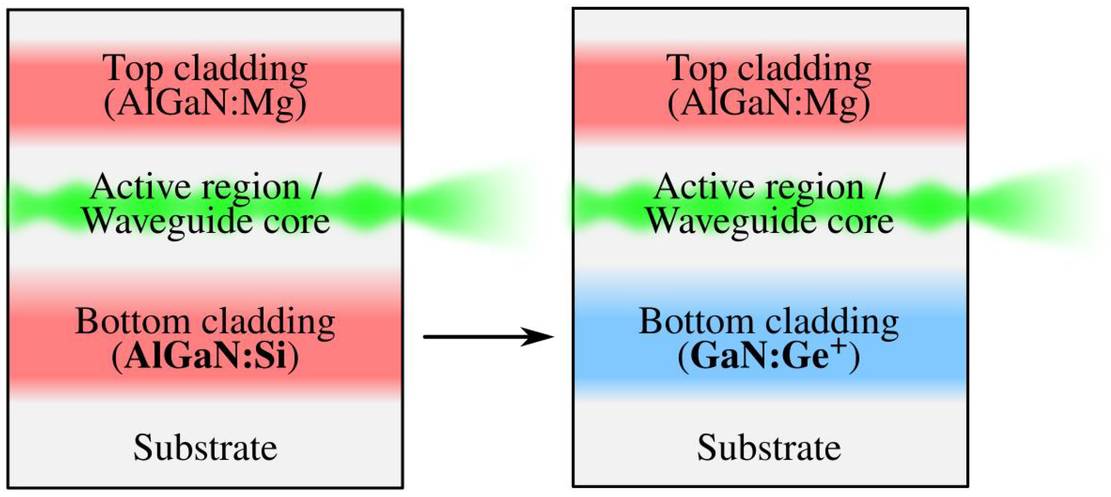
:1. Introduction
Background Work
2. Materials and Methods
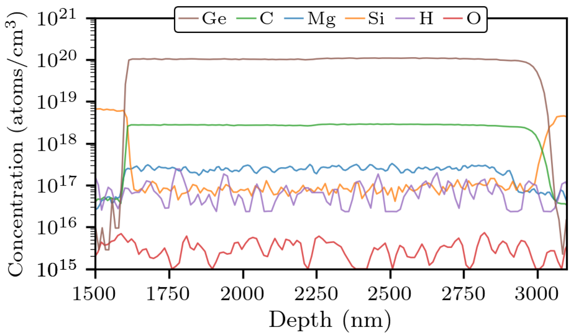
2.1. Epitaxial Growth
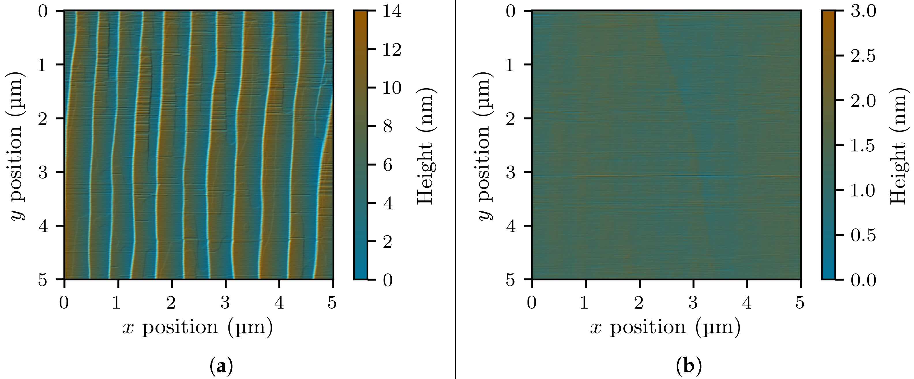
2.2. Preliminary Characterization
2.3. Reflectometry
2.4. Ellipsometry
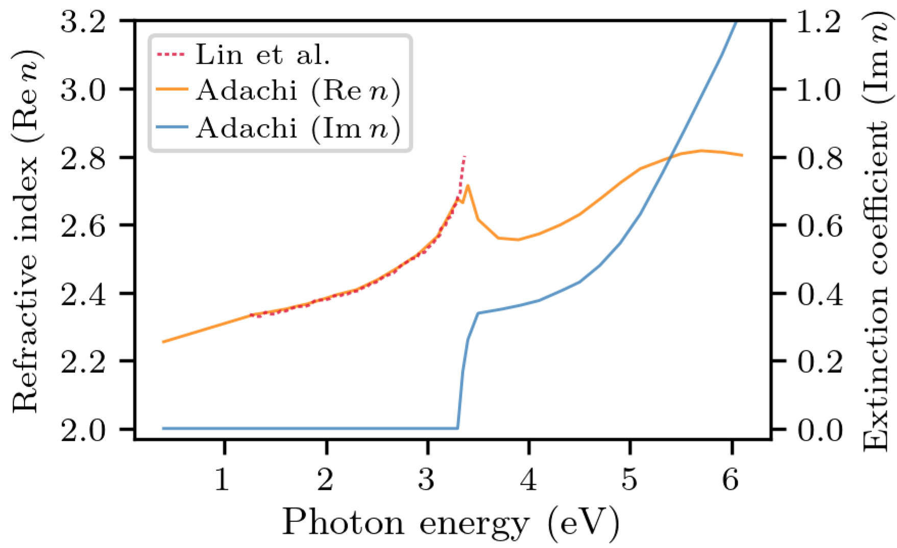
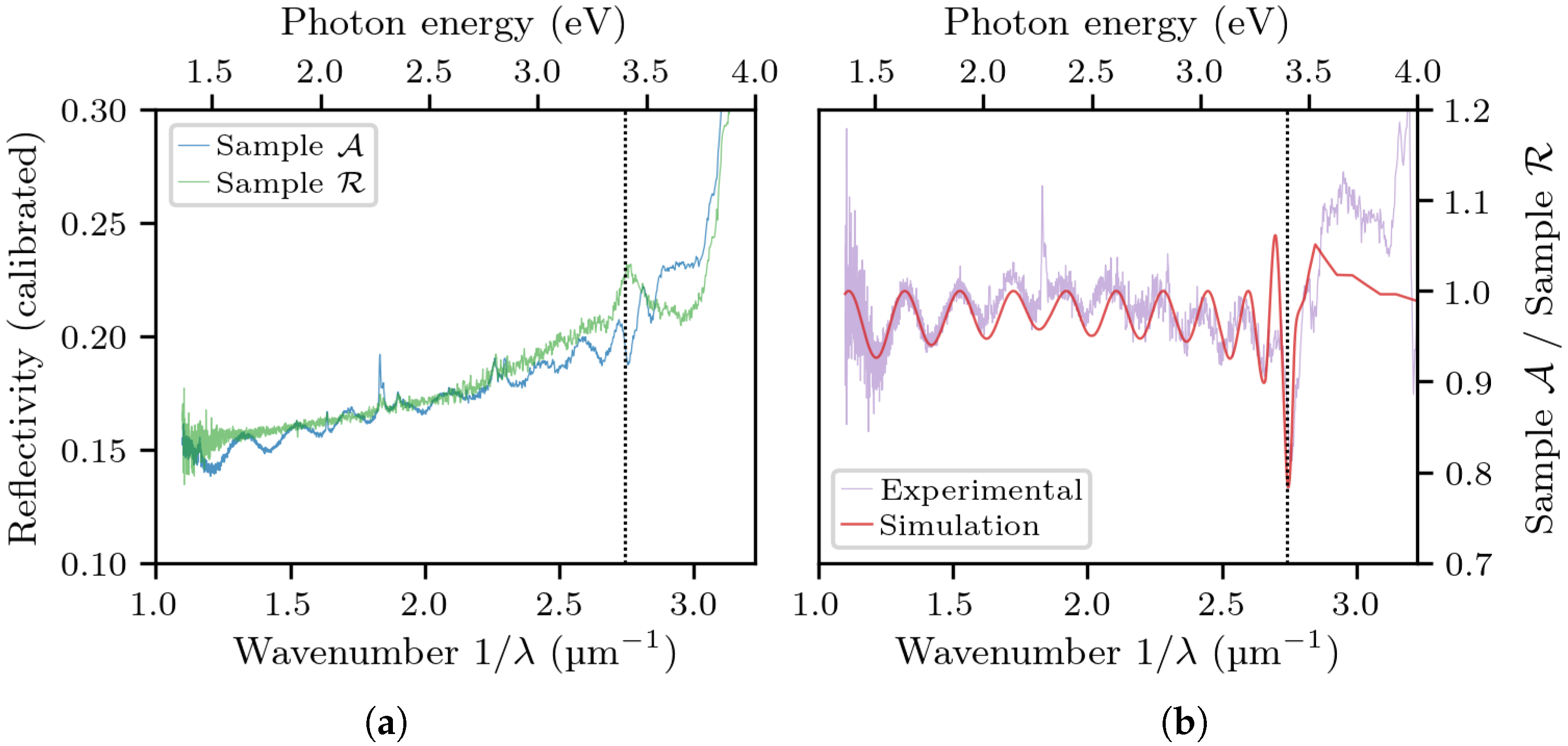
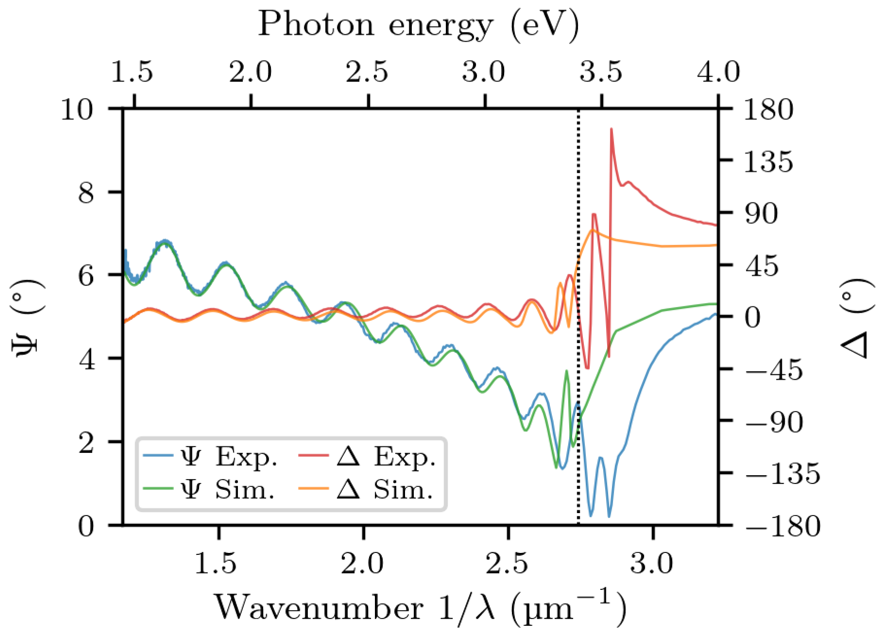
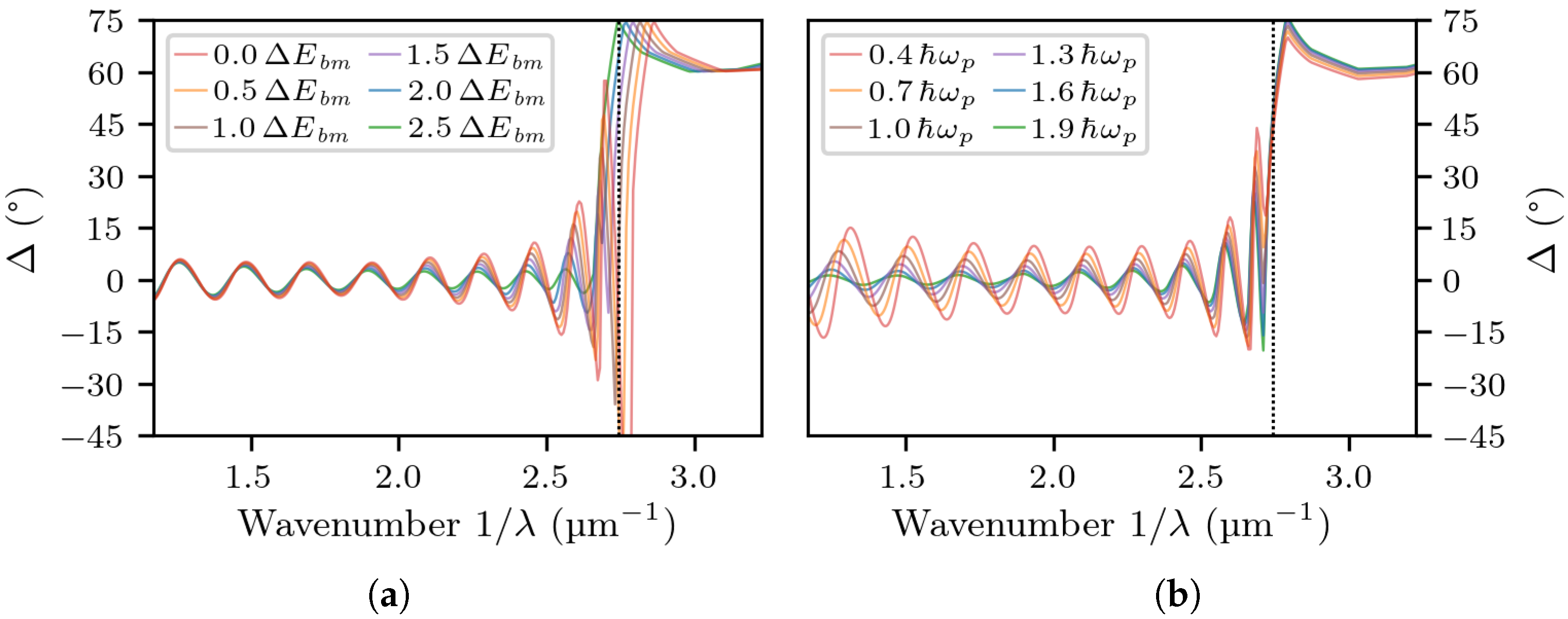
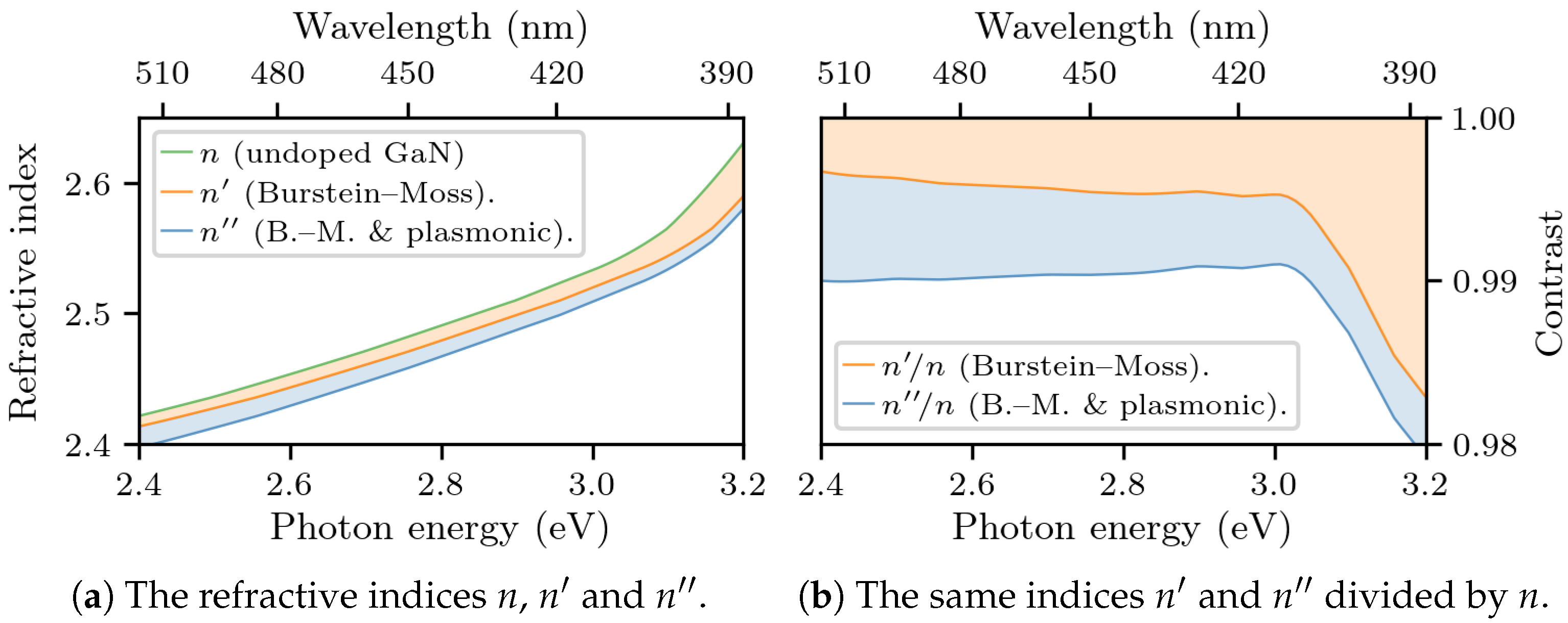
3. Results
4. Discussion
5. Conclusions
Author Contributions
Funding
Data Availability Statement
Conflicts of Interest
References
- Schwarz, U.T. Physics and Technology of AlGaInN-Based Laser Diode. In Digital Encyclopedia of Applied Physics; John Wiley & Sons, Ltd.: Hoboken, NJ, USA, 2021; pp. 1–32. [Google Scholar] [CrossRef]
- Sanford, N.A.; Robins, L.H.; Davydov, A.V.; Shapiro, A.; Tsvetkov, D.V.; Dmitriev, A.V.; Keller, S.; Mishra, U.K.; DenBaars, S.P. Refractive index study of AlxGa1-xN films grown on sapphire substrates. J. Appl. Phys. 2003, 94, 2980–2991. [Google Scholar] [CrossRef]
- Sarzyński, M.; Kryśko, M.; Targowski, G.; Czernecki, R.; Sarzyńska, A.; Libura, A.; Krupczyński, W.; Perlin, P.; Leszczyński, M. Elimination of AlGaN epilayer cracking by spatially patterned AlN mask. Appl. Phys. Lett. 2006, 88, 121124. [Google Scholar] [CrossRef]
- Berggren, K.F.; Sernelius, B.E. Band-gap narrowing in heavily doped many-valley semiconductors. Phys. Rev. B 1981, 24, 1971–1986. [Google Scholar] [CrossRef]
- Feneberg, M.; Osterburg, S.; Lange, K.; Lidig, C.; Garke, B.; Goldhahn, R.; Richter, E.; Netzel, C.; Neumann, M.D.; Esser, N.; et al. Band gap renormalization and Burstein-Moss effect in silicon- and germanium-doped wurtzite GaN up to 1020cm−3. Phys. Rev. B 2014, 90, 075203. [Google Scholar] [CrossRef]
- Peter, Y.U.; Cardona, M. Fundamentals of Semiconductors: Physics and Materials Properties, 4th ed.; Graduate Texts in Physics; Springer: Berlin/Heidelberg, Germany, 2010; p. 306. [Google Scholar]
- Perlin, P.; Holc, K.; Sarzyński, M.; Scheibenzuber, W.; Marona, L.; Czernecki, R.; Leszczyński, M.; Bockowski, M.; Grzegory, I.; Porowski, S.; et al. Application of a composite plasmonic substrate for the suppression of an electromagnetic mode leakage in InGaN laser diodes. Appl. Phys. Lett. 2009, 95, 261108. [Google Scholar] [CrossRef]
- Perlin, P.; Czyszanowski, T.; Marona, L.; Grzanka, S.; Kafar, A.; Stanczyk, S.; Suski, T.; Leszczyński, M.; Boćkowski, M.; Muzioł, G.; et al. Highly Doped GaN: A Material for Plasmonic Claddings for Blue/Green InGaN Laser Diodes; Gallium Nitride Materials and Devices, VII; Chyi, J.I., Nanishi, Y., Morkoç, H., Piprek, J., Yoon, E., Eds.; International Society for Optics and Photonics, SPIE: Bellingham, WA, USA, 2012; Volume 8262, pp. 161–168. [Google Scholar] [CrossRef]
- Stańczyk, S.; Czyszanowski, T.; Kafar, A.; Czernecki, R.; Targowski, G.; Leszczyński, M.; Suski, T.; Kucharski, R.; Perlin, P. InGaN laser diodes with reduced AlGaN cladding thickness fabricated on GaN plasmonic substrate. Appl. Phys. Lett. 2013, 102, 151102. [Google Scholar] [CrossRef]
- Bockowski, M. High nitrogen pressure solution growth of GaN. Jpn. J. Appl. Phys. 2014, 53, 100203. [Google Scholar] [CrossRef] [Green Version]
- Fritze, S.; Dadgar, A.; Witte, H.; Bügler, M.; Rohrbeck, A.; Bläsing, J.; Hoffmann, A.; Krost, A. High Si and Ge n-type doping of GaN doping–Limits and impact on stress. Appl. Phys. Lett. 2012, 100, 122104. [Google Scholar] [CrossRef] [Green Version]
- Götz, W.; Kern, R.S.; Chen, C.H.; Liu, H.; Steigerwald, D.A.; Fletcher, R.M. Hall-effect characterization of III–V nitride semiconductors for high efficiency light emitting diodes. Mater. Sci. Eng. B 1999, 59, 211–217. [Google Scholar] [CrossRef]
- Oshima, Y.; Yoshida, T.; Watanabe, K.; Mishima, T. Properties of Ge-doped, high-quality bulk GaN crystals fabricated by hydride vapor phase epitaxy. J. Cryst. Growth 2010, 312, 3569–3573. [Google Scholar] [CrossRef]
- Schiavon, D.; Litwin-Staszewska, E.; Jakieła, R.; Grzanka, S.; Perlin, P. Effects of MOVPE Growth Conditions on GaN Layers Doped with Germanium. Materials 2021, 14, 354. [Google Scholar] [CrossRef]
- Nenstiel, C.; Bügler, M.; Callsen, G.; Nippert, F.; Kure, T.; Fritze, S.; Dadgar, A.; Witte, H.; Bläsing, J.; Krost, A.; et al. Germanium—The superior dopant in n-type GaN. Phys. Status Solidi RRL 2015, 9, 716–721. [Google Scholar] [CrossRef]
- Gamarra, P.; Lacam, C.; Tordjman, M.; Splettstösser, J.; Schauwecker, B.; di Forte-Poisson, M.A. Optimisation of a carbon doped buffer layer for AlGaN/GaN HEMT devices. J. Cryst. Growth 2015, 414, 232–236, Seventeenth International Conference on Metalorganic Vapor Phase Epitaxy. [Google Scholar] [CrossRef]
- Ciarkowski, T.; Allen, N.; Carlson, E.; McCarthy, R.; Youtsey, C.; Wang, J.; Fay, P.; Xie, J.; Guido, L. Connection between Carbon Incorporation and Growth Rate for GaN Epitaxial Layers Prepared by OMVPE. Materials 2019, 12, 2455. [Google Scholar] [CrossRef] [Green Version]
- Chen, Y.; Takeuchi, T.; Amano, H.; Akasaki, I.; Yamada, N.; Kaneko, Y.; Wang, S.Y. Pit formation in GaInN quantum wells. Appl. Phys. Lett. 1998, 72, 710–712. [Google Scholar] [CrossRef]
- Knetzger, M.; Meissner, E.; Schröter, C.; Friedrich, J. Theoretical aspects and microstructural investigations on V-pit defects in HVPE grown GaN. J. Cryst. Growth 2019, 518, 51–58. [Google Scholar] [CrossRef]
- Hiramatsu, K.; Amano, H.; Akasaki, I.; Kato, H.; Koide, N.; Manabe, K. MOVPE growth of GaN on a misoriented sapphire substrate. J. Cryst. Growth 1991, 107, 509–512. [Google Scholar] [CrossRef]
- Ramana Murty, M.V.; Fini, P.; Stephenson, G.B.; Thompson, C.; Eastman, J.A.; Munkholm, A.; Auciello, O.; Jothilingam, R.; DenBaars, S.P.; Speck, J.S. Step bunching on the vicinal GaN(0001) surface. Phys. Rev. B 2000, 62, R10661–R10664. [Google Scholar] [CrossRef]
- Hanser, D.; Tutor, M.; Preble, E.; Williams, M.; Xu, X.; Tsvetkov, D.; Liu, L. Surface preparation of substrates from bulk GaN crystals. J. Cryst. Growth 2007, 305, 372–376. [Google Scholar] [CrossRef]
- Lin, M.E.; Sverdlov, B.N.; Strite, S.; Morkoç, H.; Drakin, A.E. Refractive Indices of Wurtzite and Zincblende GaN. Electron. Lett. 1993, 29, 1759–1760. Available online: https://refractiveindex.info (accessed on October 2021). [CrossRef]
- Adachi, S. Optical Constants of Crystalline and Amorphous Semiconductors: Numerical Data and Graphical Information; Springer: Boston, MA, USA, 2013; pp. 186–187. Available online: https://www.filmetrics.com (accessed on October 2021).
- Kirste, R.; Hoffmann, M.P.; Sachet, E.; Bobea, M.; Bryan, Z.; Bryan, I.; Nenstiel, C.; Hoffmann, A.; Maria, J.P.; Collazo, R.; et al. Ge doped GaN with controllable high carrier concentration for plasmonic applications. Appl. Phys. Lett. 2013, 103, 242107. [Google Scholar] [CrossRef]


Publisher’s Note: MDPI stays neutral with regard to jurisdictional claims in published maps and institutional affiliations. |
© 2021 by the authors. Licensee MDPI, Basel, Switzerland. This article is an open access article distributed under the terms and conditions of the Creative Commons Attribution (CC BY) license (https://creativecommons.org/licenses/by/4.0/).
Share and Cite
Schiavon, D.; Mroczyński, R.; Kafar, A.; Kamler, G.; Levchenko, I.; Najda, S.; Perlin, P. Refractive Index of Heavily Germanium-Doped Gallium Nitride Measured by Spectral Reflectometry and Ellipsometry. Materials 2021, 14, 7364. https://doi.org/10.3390/ma14237364
Schiavon D, Mroczyński R, Kafar A, Kamler G, Levchenko I, Najda S, Perlin P. Refractive Index of Heavily Germanium-Doped Gallium Nitride Measured by Spectral Reflectometry and Ellipsometry. Materials. 2021; 14(23):7364. https://doi.org/10.3390/ma14237364
Chicago/Turabian StyleSchiavon, Dario, Robert Mroczyński, Anna Kafar, Grzegorz Kamler, Iryna Levchenko, Stephen Najda, and Piotr Perlin. 2021. "Refractive Index of Heavily Germanium-Doped Gallium Nitride Measured by Spectral Reflectometry and Ellipsometry" Materials 14, no. 23: 7364. https://doi.org/10.3390/ma14237364
APA StyleSchiavon, D., Mroczyński, R., Kafar, A., Kamler, G., Levchenko, I., Najda, S., & Perlin, P. (2021). Refractive Index of Heavily Germanium-Doped Gallium Nitride Measured by Spectral Reflectometry and Ellipsometry. Materials, 14(23), 7364. https://doi.org/10.3390/ma14237364