Electrical and Optical Characterization of Sputtered Silicon Dioxide, Indium Tin Oxide, and Silicon Dioxide/Indium Tin Oxide Antireflection Coating on Single-Junction GaAs Solar Cells


Abstract
:1. Introduction
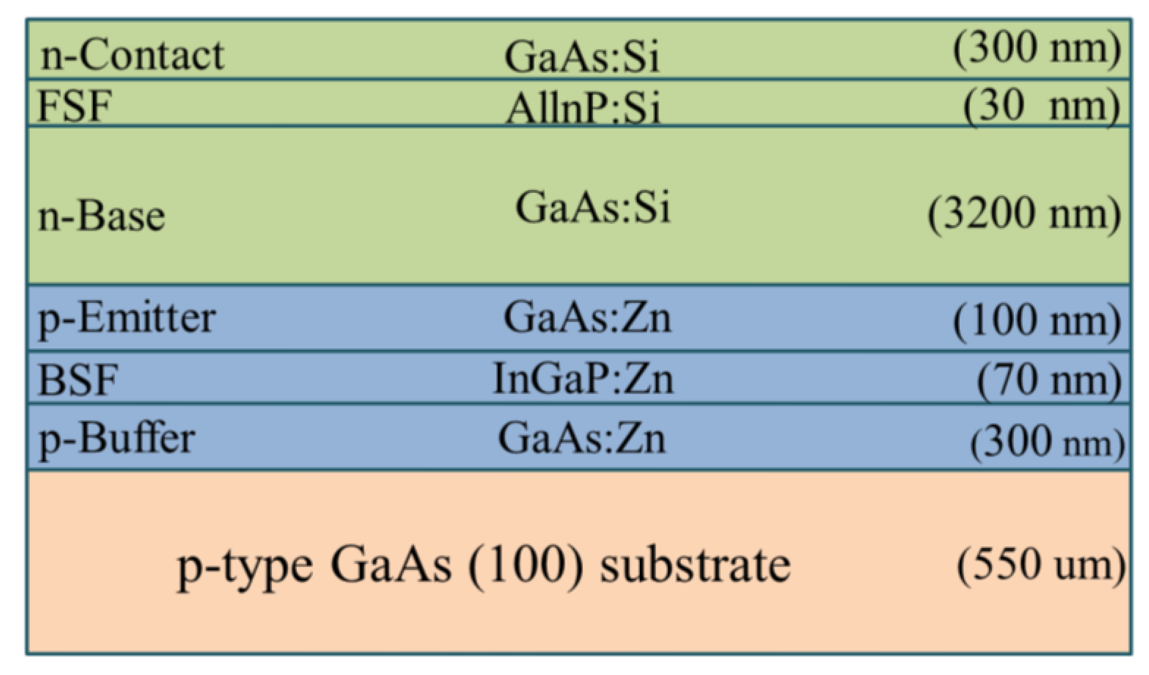
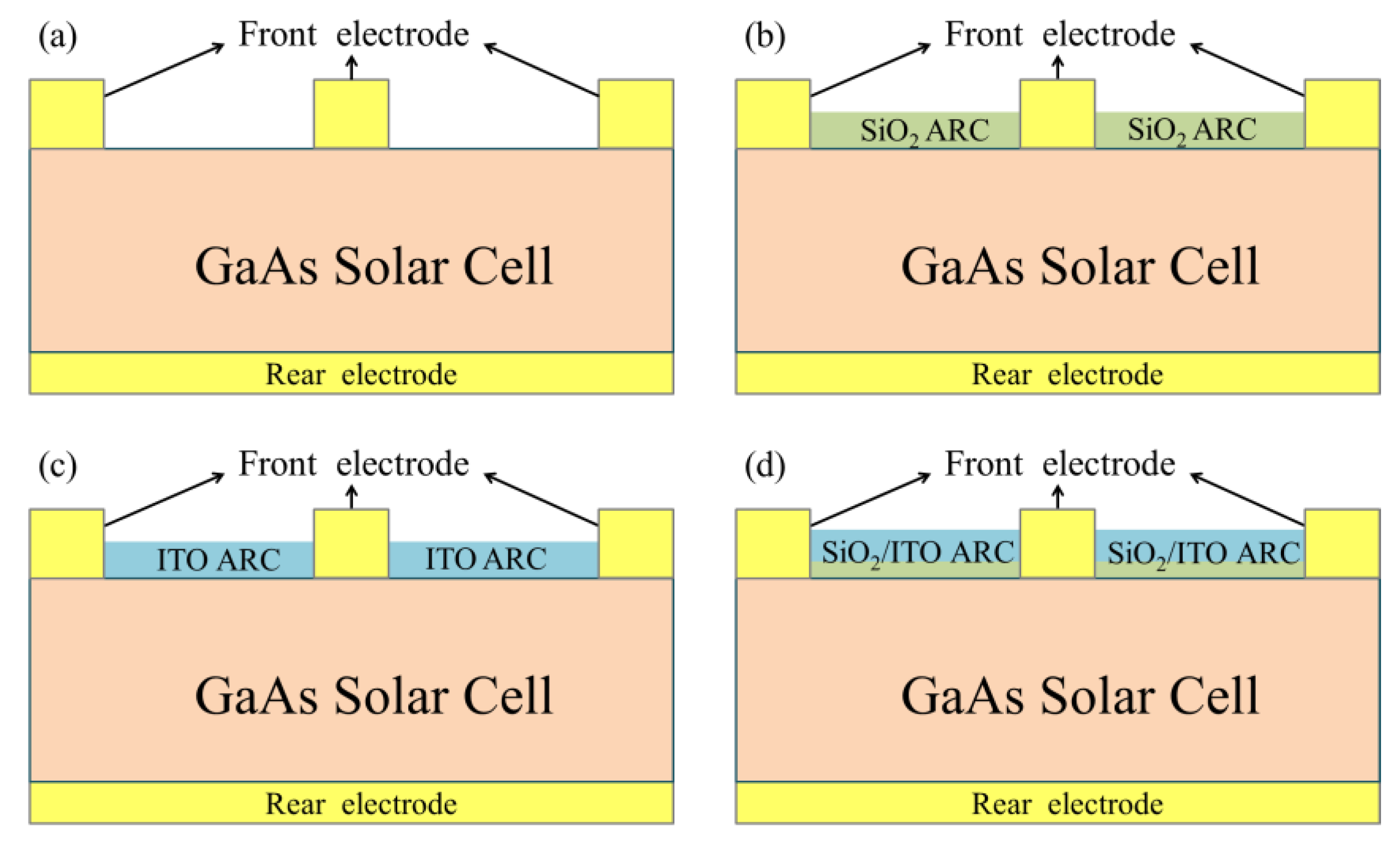
2. Experiments
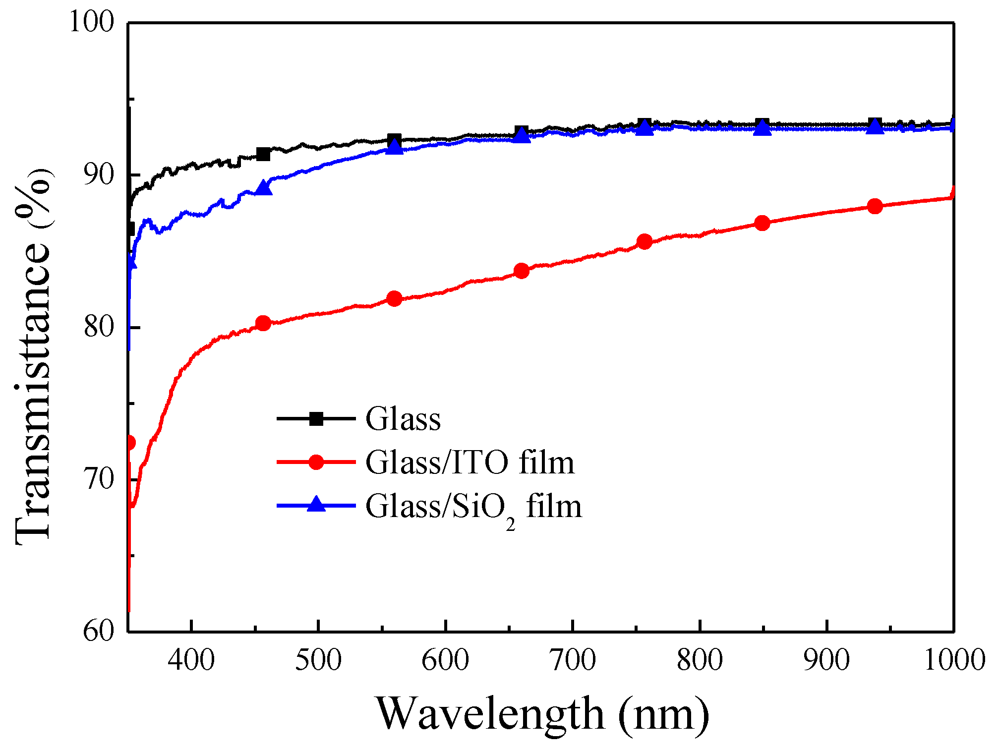
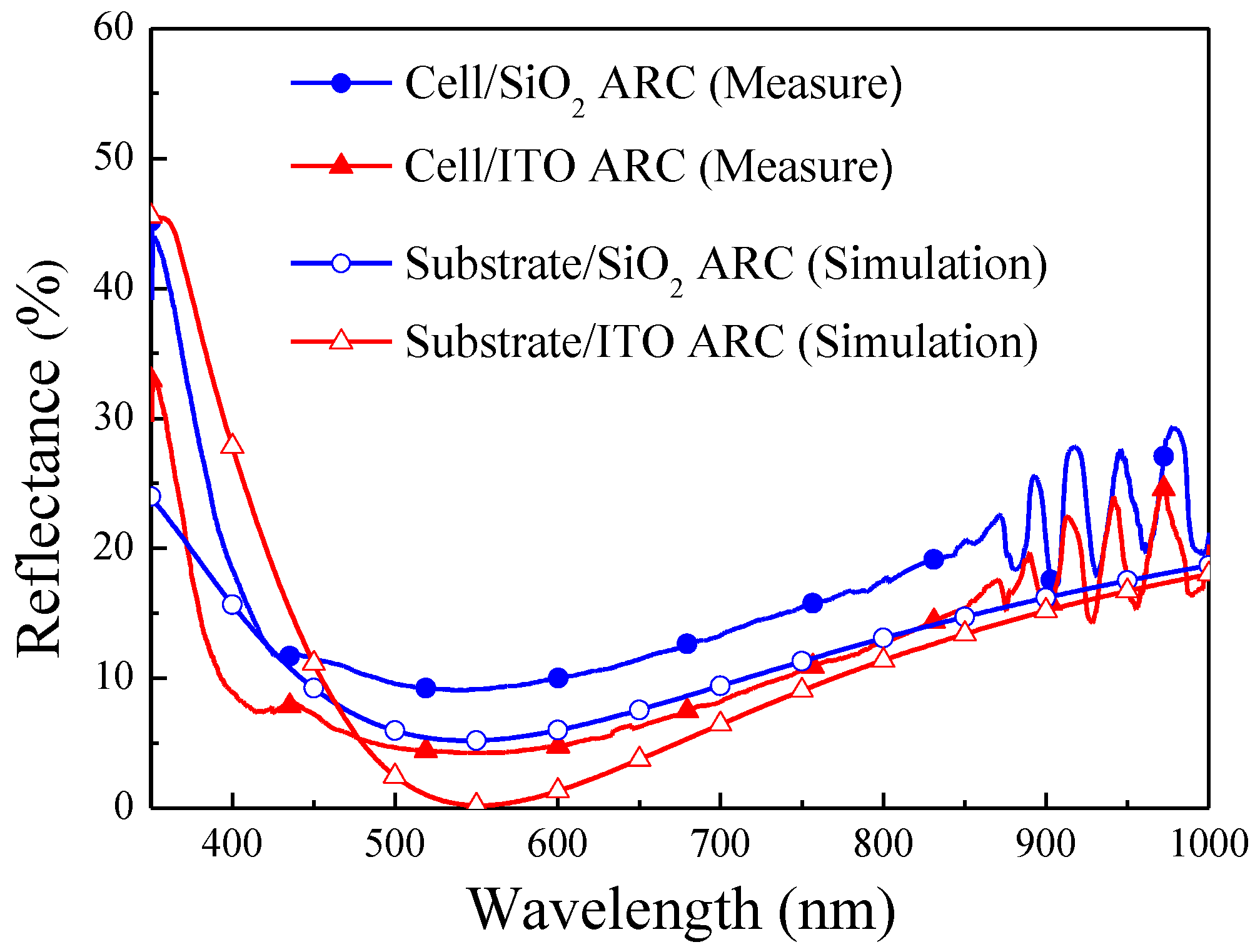
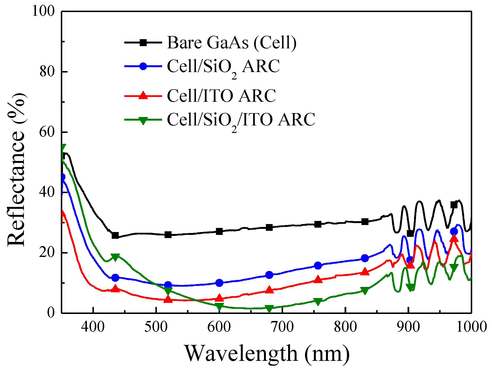
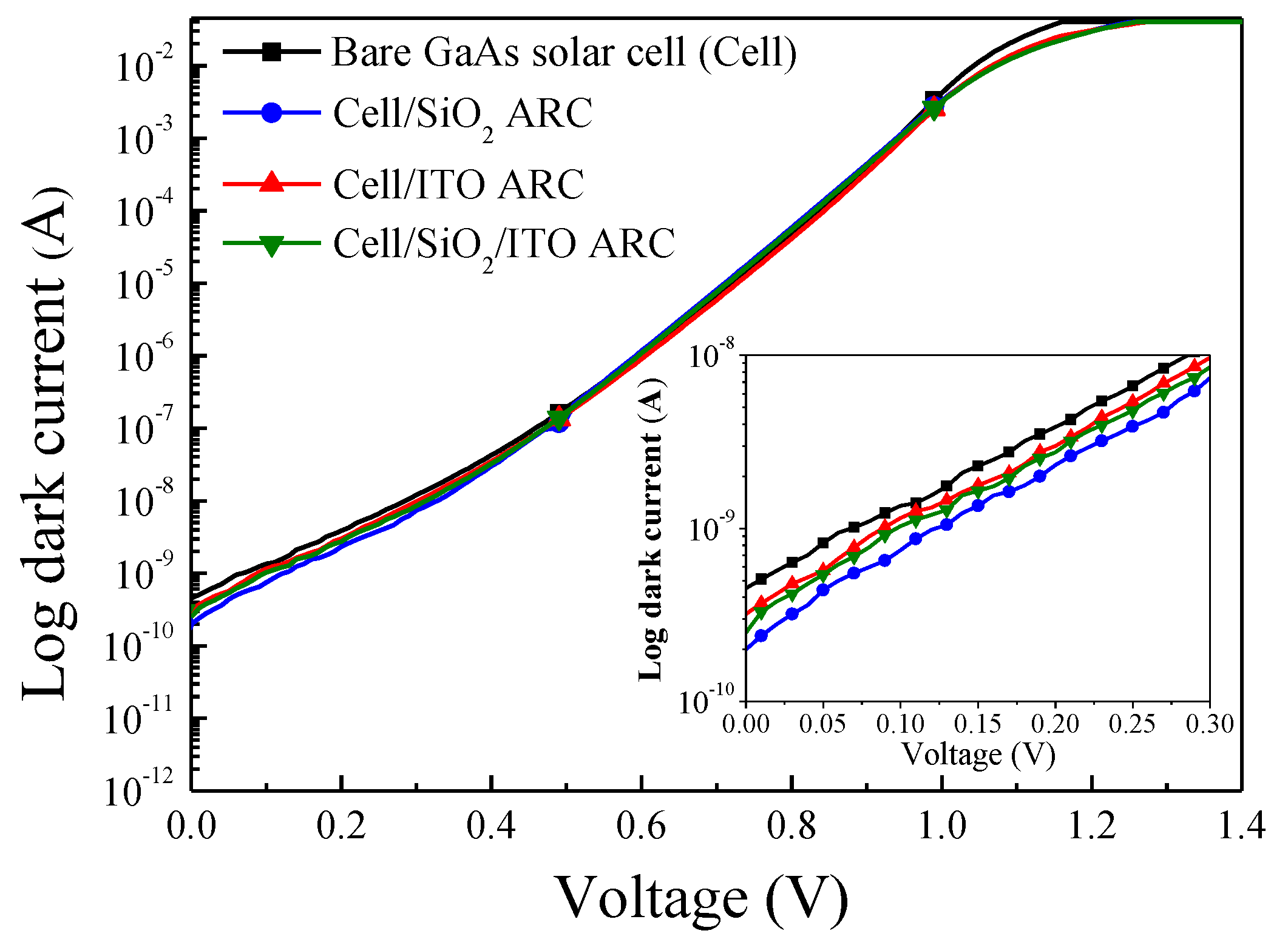
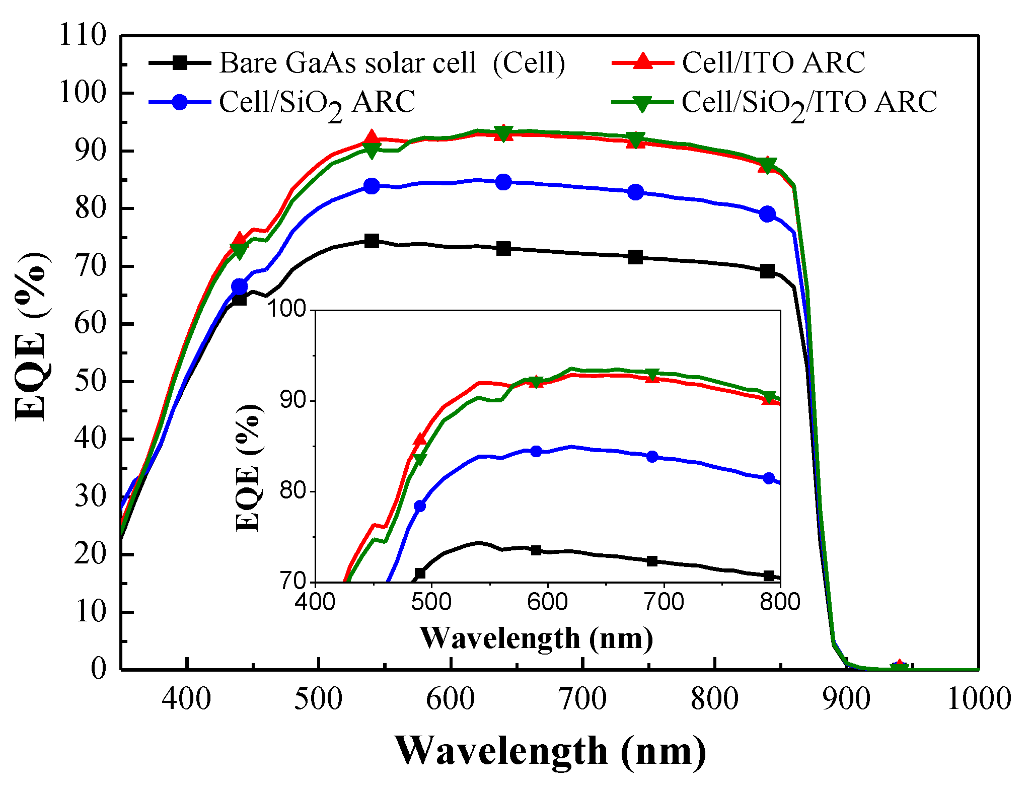
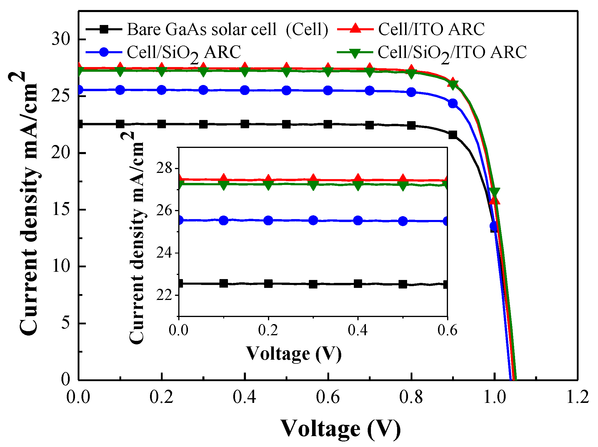
3. Results and Discussion
4. Conclusions
Acknowledgments
Author Contributions
Conflicts of Interest
References
- Farhan, M.S.; Zalnezhad, E.; Bushroa, A.R.; Sarhan, A.A.D. Electrical and optical properties of indium-tin oxide (ITO) films by in-assisted deposition (IAD) at room temperature. Int. J. Precision Eng. Manuf. 2013, 14, 1465–1469. [Google Scholar] [CrossRef]
- Wang, M.; Diao, X.; Dong, G.; He, Y.; Liu, Q. Optical, electrical, and electrochemical properties of indium tin oxide thin films studied in different layer-structures and their corresponding inorganic all-thin-film solid-state electrochromic devices. J. Vac. Sci. Technol. A 2017. [Google Scholar] [CrossRef]
- Du, J.; Chen, X.; Liu, C.; Ni, J.; Hou, G.; Zhao, Y.; Zhang, X. Highly transparent and conductive indium tin oxide thin films for solar cells grown by reactive thermal evaporation at low temperature. Appl. Phys. A 2014, 117, 815–822. [Google Scholar] [CrossRef]
- Minami, T. Transparent conducting oxide semiconductors for transparent electrodes. Semicond. Sci. Technol. 2005, 20, S35–S44. [Google Scholar] [CrossRef]
- Cao, W.; Li, J.; Chen, H.; Xue, J. Transparent electrodes for organic optoelectronic devices: A review. J. Photonics Energy 2014, 4, 040990:1–040990:28. [Google Scholar] [CrossRef]
- Hamelmann, F.U. Transparent conductive cxides in thin film photovoltaics. J. Phys. Conf. Ser. 2014, 559, 012016:1–012016:9. [Google Scholar] [CrossRef]
- Selja, J.K.; Young, D.; Grover, S. Optimization of the antireflection coating of thin epitaxial crystalline silicon solar cells. Energy Procedia 2015, 77, 248–252. [Google Scholar] [CrossRef]
- Lien, S.Y. Characterization and optimization of ITO thin films for application in heterojunction silicon solar cells. Thin Solid Films 2010, 518, S10–S13. [Google Scholar] [CrossRef]
- Boscarino, S.; Crupi, I.; Mirabella, S.; Simone, F.; Terrasi, A. TCO/Ag/TCO transparent electrodes for solar cells application. Appl. Phys. A 2014, 116, 1287–1291. [Google Scholar] [CrossRef]
- Kudryashov, D.; Gudovskikh, A.; Zelentsov, K. Low temperature growth of ITO transparent conductive oxide layers in oxygen-free environment by RF magnetron sputtering. J. Phys. Conf. Ser. 2013, 461, 012021:1–012021:5. [Google Scholar] [CrossRef]
- Jung, T.D.; Song, P.K. Mechanical and structural properties of high temperature a-ITO: Sm films deposited on polyimide substrate by DC magnetron sputtering. Curr. Appl. Phys. 2011, 11, S314–S319. [Google Scholar] [CrossRef]
- Jung, S.K.; Lee, S.H.; Lee, Y.S.; Lee, S.M.; Park, L.S.; Sohn, S.H. Effects of temperature on ITO Films grown by low frequency (60 Hz) magnetron sputtering. Mol. Cryst. Liq. Cryst. 2009, 499, 316–324. [Google Scholar] [CrossRef]
- Baia, I.; Quintelab, M.; Mendesa, L.; Nunesa, P.; Martins, R. Performances exhibited by large area ITO layers produced by r.f. magnetron sputtering. Thin Solid Films 1999, 337, 171–175. [Google Scholar] [CrossRef]
- Canhola, P.; Martins, N.; Raniero, L.; Pereira, S.; Fortunato, E.; Ferreira, I.; Martins, R. Role of annealing environment on the performances of large area ITO films produced by rf magnetron sputtering. Thin Solid Films 2005, 487, 271–276. [Google Scholar] [CrossRef]
- Lin, H.H.; Lee, S.C. Super-gain AlGaAs/GaAs heterojunction bipolar transistors using an emitter edge-thinning design. Appl. Phys. Lett. 1985, 47, 839–841. [Google Scholar] [CrossRef]
- Kuzuhara, M.; Tanaka, S. GaAs-based high-frequency and high-speed devices. JSAP Int. 2003, 7, 1–11. [Google Scholar]
- Shimawaki, H.; Kawanaka, M.; Goto, N. Microwave Noise Characteristics of GaAs Based HBTs. In Proceedings of the Gigahertz Devices and Systems, Boston, MA, USA, 20 September 1999; Volume 3861, pp. 1–10. [Google Scholar] [CrossRef]
- Schwierz, F.; Liou, J.J. RF transistors: Recent developments and roadmap toward terahertz applications. Solid-State Electron. 2007, 51, 1079–1091. [Google Scholar] [CrossRef]
- Moon, S.; Kim, K.; Kim, Y.; Heo, J.; Lee, J. Highly efficient single-junction GaAs thin-film solar cell on flexible substrate. Sci. Rep. 2016, 6, 1–6. [Google Scholar] [CrossRef] [PubMed]
- Kim, K.; Nguyen, H.D.; Mho, S.; Lee, J. Enhanced efficiency of GaAs single-junction solar cells with inverted-cone-shaped nanoholes fabricated using anodic aluminum oxide masks. Int. J. Photoenergy 2013. [Google Scholar] [CrossRef]
- Ringel, S.A.; Carlin, J.A.; Andre, C.L.; Hudait, M.K.; Gonzalez, M.; Wilt, D.M.; Clark, E.B.; Jenkins, P.; Scheiman, D.; Allerman, A.; et al. Single-junction InGaP/GaAs solar cells grown on Si substrates with SiGe buffer layers. Prog. Photovolt. Res. Appl. 2002, 10, 417–426. [Google Scholar] [CrossRef]
- O’Connor, J.E.; Michael, S. A novel thin-film, single-junction solar cell design to achieve power conversion efficiency above 30 percent. Mater. Sci. Appl. 2016, 7, 823–835. [Google Scholar] [CrossRef]
- Mariani1, G.; Scofield, A.C.; Hung, C.-H.; Huffaker, D.L. GaAs nanopillar-array solar cells employing in situ surface passivation. Nat. Commun. 2013, 4, 1–10. [Google Scholar] [CrossRef]
- Ba, O.; Mbengue, N.; Dia, F.; Diaw, A.; Diop, M.M.; Ba, B.; Barro, F.I. Graded SiNx/SiOxNy layers as antireflective coatings for solar cells based on GaAs and silicon crystalline. Sci. Res. 2016, 4, 21–25. [Google Scholar] [CrossRef]
- Saylan, S.; Milakovich, T.; Hadi, S.A.; Nayfeh, A.; Fitzgerald, E.A.; Dahlem, M.S. Multilayer antireflection coating design for GaAs0.69P0.31/Si dual-junction solar cells. Sol. Energy 2015, 122, 76–86. [Google Scholar] [CrossRef]
- Teran, A.S; Moon, E.; Lim, W.; Kim, G.; Lee, I.; Blaauw, D.; Phillips, J.D. Energy harvesting for GaAs photovoltaics under low-flux indoor lighting conditions. IEEE Trans. Electron Devices 2016, 63, 2820–2825. [Google Scholar] [CrossRef] [PubMed]
- Sheldon, P.; Hayes, R.E.; Russell, P.E.; Nottenburg, R.N.; Emery, K.A.; Ireland, P.J.; Kazmerskiless, L.L. Evaluation of ITO/GaAs solar cells. J. Vac. Sci. Technol. 1982, 20, 410. [Google Scholar] [CrossRef]
- Dai, P.; Lu, J.; Tan, M.; Wang, Q.; Wu, Y.; Ji, L.; Bian, L.; Lu, S.; Yang, H. Transparent conducting indium-tin-oxide (ITO) film as full front electrode in III–V compound solar cell. Chin. Phys. B 2017, 26, 037305:1–037305:5. [Google Scholar] [CrossRef]


| Parameters | Bare GaAs (Cell) | Cell/SiO2 ARC | Cell/ITO ARC | Cell/SiO2/ITO ARC |
|---|---|---|---|---|
| J0 (A/cm2) | 1.27 × 10⁻¹⁰ | 7.60 × 10⁻¹¹ | 9.55 × 10⁻¹¹ | 7.68 × 10⁻¹¹ |
| n | 2.46 | 2.32 | 2.42 | 2.34 |
| RW (%) | 29.62 | 15.14 | 9.29 | 8.90 |
| EQEw (%) | 59.03 | 66.18 | 72.43 | 71.87 |
| Jsc (mA/cm2) | 22.47 | 25.55 | 27.47 | 27.25 |
| Voc (V) | 1.05 | 1.04 | 1.05 | 1.05 |
| Rs (Ω) | 3.64 | 3.58 | 2.55 | 3.39 |
| Rsh (Ω) | 3.93 × 10⁴ | 5.43 × 10⁵ | 2.10 × 10⁵ | 3.05 × 10⁵ |
| FF (%) | 81.68 | 82.57 | 81.93 | 81.98 |
| η (%) | 19.27 | 21.92 | 23.52 | 23.48 |
© 2017 by the authors. Licensee MDPI, Basel, Switzerland. This article is an open access article distributed under the terms and conditions of the Creative Commons Attribution (CC BY) license (http://creativecommons.org/licenses/by/4.0/).
Share and Cite
Ho, W.-J.; Lin, J.-C.; Liu, J.-J.; Bai, W.-B.; Shiao, H.-P. Electrical and Optical Characterization of Sputtered Silicon Dioxide, Indium Tin Oxide, and Silicon Dioxide/Indium Tin Oxide Antireflection Coating on Single-Junction GaAs Solar Cells. Materials 2017, 10, 700. https://doi.org/10.3390/ma10070700
Ho W-J, Lin J-C, Liu J-J, Bai W-B, Shiao H-P. Electrical and Optical Characterization of Sputtered Silicon Dioxide, Indium Tin Oxide, and Silicon Dioxide/Indium Tin Oxide Antireflection Coating on Single-Junction GaAs Solar Cells. Materials. 2017; 10(7):700. https://doi.org/10.3390/ma10070700
Chicago/Turabian StyleHo, Wen-Jeng, Jian-Cheng Lin, Jheng-Jie Liu, Wen-Bin Bai, and Hung-Pin Shiao. 2017. "Electrical and Optical Characterization of Sputtered Silicon Dioxide, Indium Tin Oxide, and Silicon Dioxide/Indium Tin Oxide Antireflection Coating on Single-Junction GaAs Solar Cells" Materials 10, no. 7: 700. https://doi.org/10.3390/ma10070700
APA StyleHo, W.-J., Lin, J.-C., Liu, J.-J., Bai, W.-B., & Shiao, H.-P. (2017). Electrical and Optical Characterization of Sputtered Silicon Dioxide, Indium Tin Oxide, and Silicon Dioxide/Indium Tin Oxide Antireflection Coating on Single-Junction GaAs Solar Cells. Materials, 10(7), 700. https://doi.org/10.3390/ma10070700