2.1. Properties of As-Deposited ZnO:Al Films
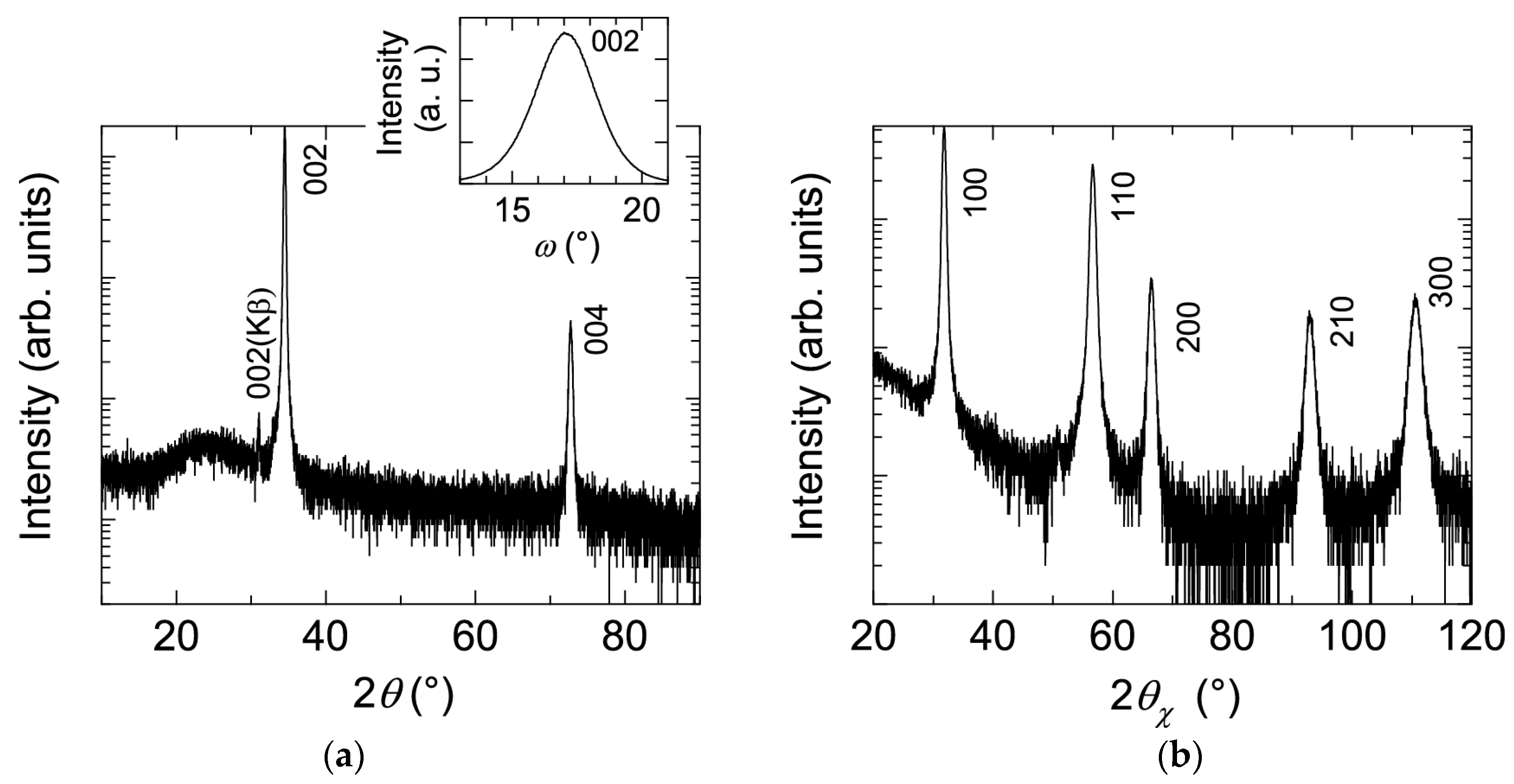
Figure 1 shows (a)
θ–2
θ scan (out-of-plane) with 002
ω scan and (b) 2
θx–
ϕ scan (in-plane) X-ray diffraction (XRD) patterns of a ~240-nm-thick ZnO:Al (2.0 wt %) film grown at 250 °C as an example. Only the diffraction peaks due to (002) and (004) planes were observed in the
θ–2
θ scan, whereas the diffraction peaks due to (100), (110), (200), (210), and (300) planes were observed. All of the prepared films with various Al contents and
Tg exhibited preferred orientation of the
c-axis normal to the substrate plane and did not contain any additional phases (e.g., ZnAl
2O
4 or Al
2O
3 phases). Because the solid solubility limit of Al in Al
2O
3-doped ZnO sintered body prepared at 1400 °C was reported to be ~0.3 at % [
13], the ZnO:Al films fabricated in this study are metastable from a thermodynamic point of view, and a supersaturated solid solution occurs as a result of the highly non-equilibrium growth process.
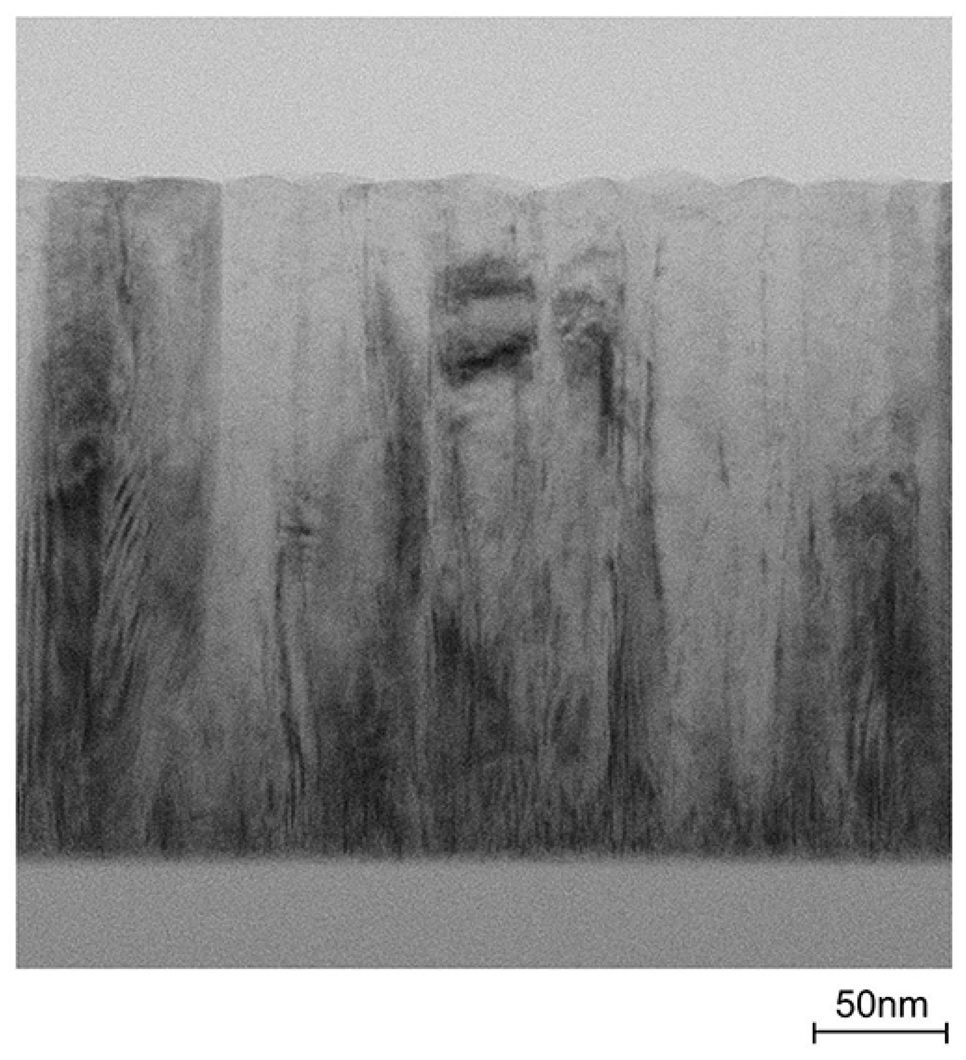
Figure 2 shows a cross-sectional transmission electron microscopy (TEM) image of the ZnO:Al (2.0 wt %) film. Abundant small columnar grains were present at the interface between the film and substrate, which had slightly tilted long-axis orientations normal to the substrate surface. For film thicknesses above 50 nm, the small grains became connected, and the deviation of each columnar grain decreased. Consequently, relatively large columnar grains with widths of 20–40 nm appeared when the film thickness exceeded 100 nm.
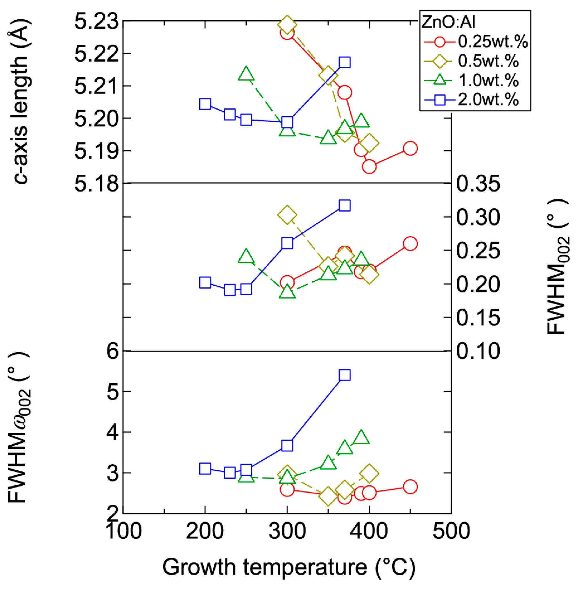
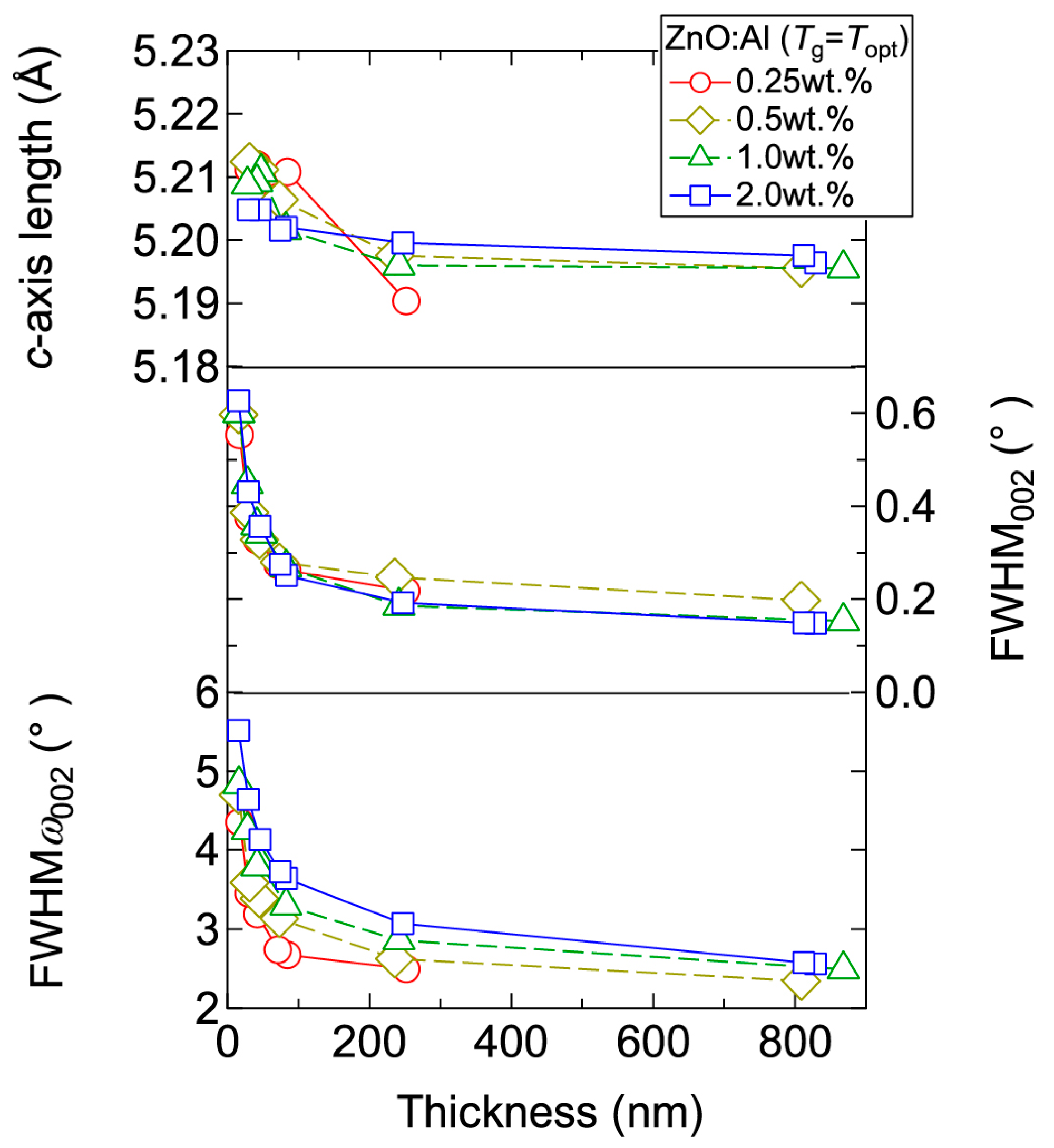
Figure 3 displays plots of the
c-axis length, the full width at half maximum (FWHM) of the 002 diffraction peak (FWHM
002), and the FWHM of rocking curves for the 002 diffraction peak (FWHM
ω002) as a function of
Tg for the ~240-nm-thick ZnO:Al films. Here, FWHM
002 reflects the out-of-plane crystallite size and the differences in
c-axis length along the growth direction due to non-uniform micro-stresses, whereas FWHM
ω002 reflects the
c-axis tilt. For each ZnO:Al film with a given Al content, FWHM
002 and FWHM
ω002 decreased gradually with increasing
Tg up to a certain optimal temperature (
Topt), while these values increased above
Topt. The values of
Topt were 250, 300, 350, and 370 °C for ZnO:Al films fabricated using ZnO ceramic targets containing 2.0, 1.0, 0.5, and 0.25 wt % Al
2O
3, respectively.
Topt decreases with increasing Al content. The variation of the FWHM values can be explained as follows: The diffusion length of adatoms and precursors at the growth surface increase with
Tg up to
Topt, thereby leading to greater crystallinity in the films. Conversely, further increases in
Tg would significantly promote diffusion of the adatoms and precursors, leading to migration of ions in the bulk films, and desorption of Zn at the growth surface. Consequently, excess Al may degrade the film crystallinity by forming local atomic structures similar to a homologous phase ((ZnO)
mAl
2O
3) [
14,
15]. The effect of inserting homologous phases in a ZnO film would be to increase the out-of-plane dimension of the film. Indeed, we observed an increase in the
c-axis length at
Tg above
Topt (
Figure 3).
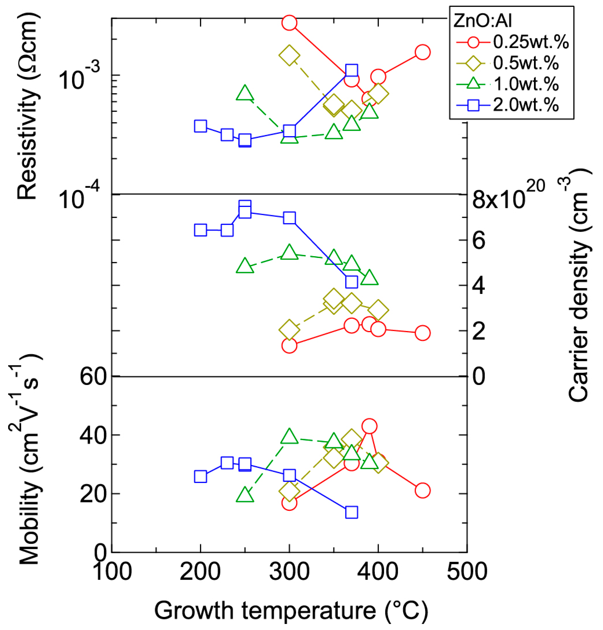
Figure 4 displays the resistivity (
ρ),
n, and
μ of the films plotted as a function of
Tg. With decreasing Al content,
n monotonically decreased along with a gradual increase in
μ. Consequently,
ρ gradually increased with decreasing Al content. More importantly, in each ZnO:Al (0.25, 0.5, 1.0, and 2.0 wt %) film, both
n and
μ exhibited maximum values at the
Topt values indicated in
Figure 3. The results suggest that imperfections of crystal are the cause of carrier trapping and scattering. This phenomenon is also observed in ZnO:Al films prepared at different film thicknesses.
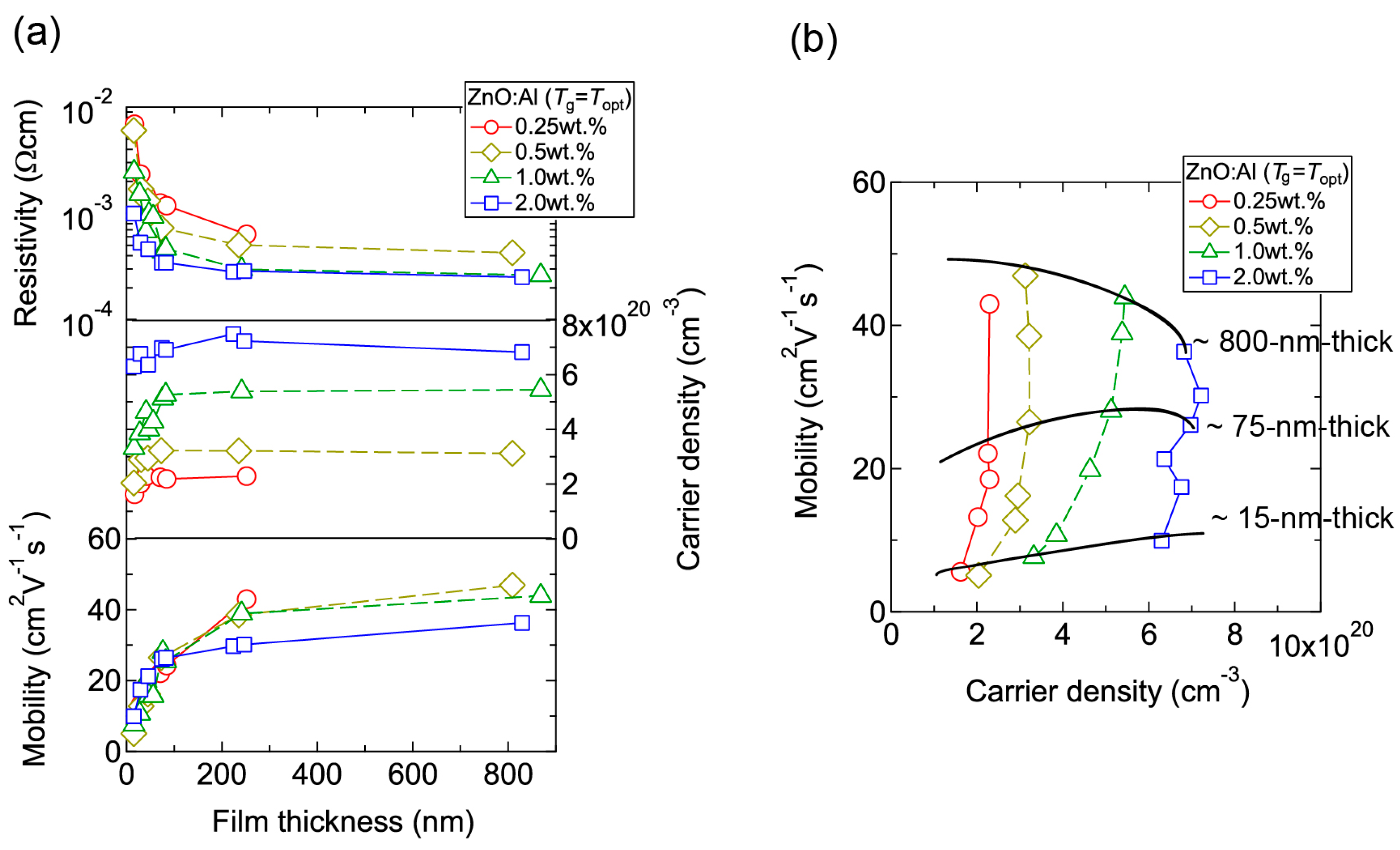
Figure 5 shows
c-axis length, FWHM
002, and FWHM
ω002 as a function of film thickness for each ZnO:Al film deposited at
Topt. Regardless of Al content, both FWHM
002 and FWHM
ω002 decreased rapidly with increasing film thickness up to 100–200 nm, and decreased gradually over 100–200 nm. Corresponding to the change in crystalline quality, both
n and
μ increased rapidly with increasing film thickness up to 100–200 nm, and increased gradually over 100–200 nm for each ZnO:Al (0.25, 0.5, 1.0, and 2.0 wt %), as shown in
Figure 6a.
Figure 6b plots a relationship between
n and
μ. In
Figure 6b, thick solid lines are connected to the films having similar film thicknesses. In general, mobility of degenerated semiconductors decreases with increase in carrier density, since donor impurities work as scattering centers of free carriers. Indeed, measured
μ for thick films with a thickness of ~800 nm decreased with an increase in Al content or
n. However, for thin films with a thickness of less than 100 nm, mobility increased with carrier density. The behavior can be explained on the basis of scattering at the grain boundary (GB) rather than ionized impurities [
16,
17]. GB scattering is described by the Seto model, in which the mobility is dominated by thermionic emission across grain barriers, where impurities or other defects induce electron traps at GBs [
16]. For films with very high
n values, the depletion width formed at a GB is narrow, enabling tunneling through the barriers by free electrons. These results shown in
Figure 3,
Figure 4,
Figure 5 and
Figure 6 clearly indicate that imperfections in the crystal lattice and concentration of GB are the cause of carrier trapping and scattering. It should be noted that the values of
n,
μ, and
Topt obtained for each ZnO:Al are comparable to those previously reported for ZnO:Al films [
11,
12,
18].
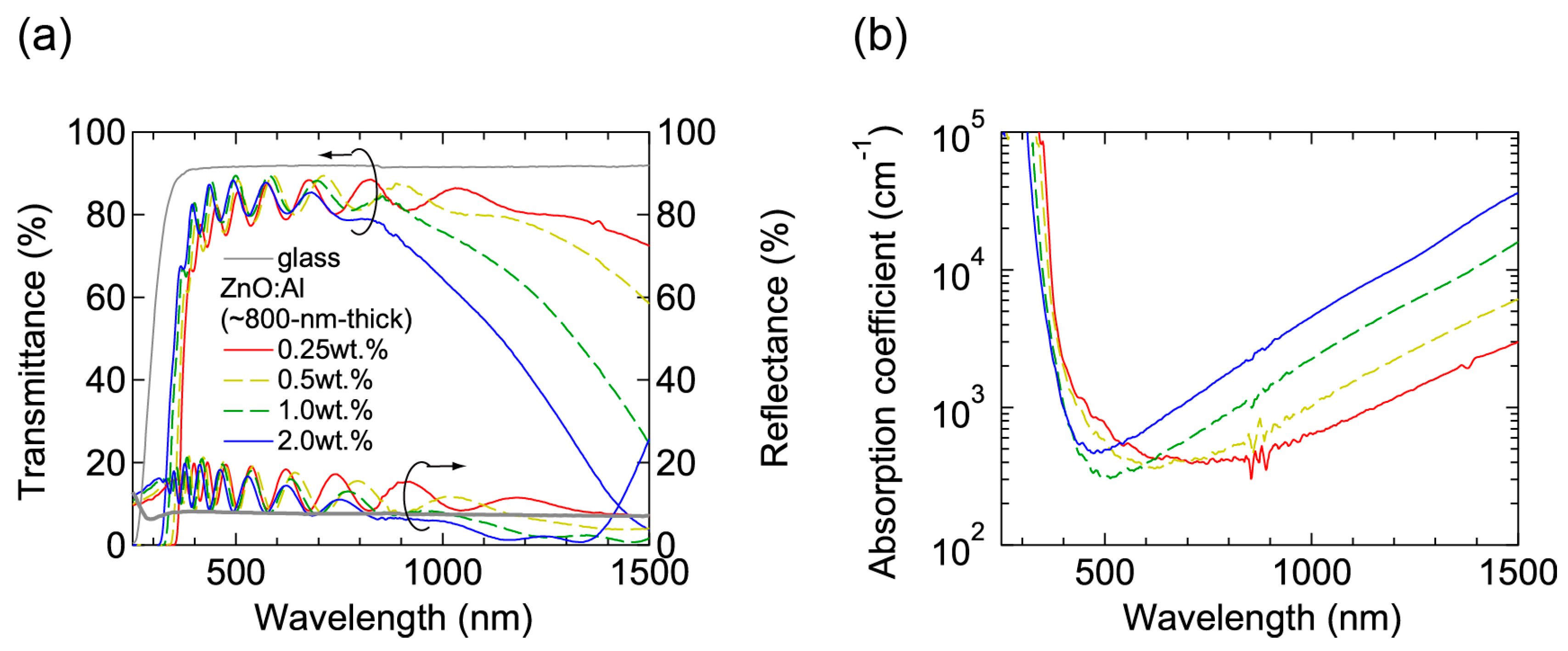
Figure 7 shows (a) transmittance and reflectance; and (b) absorption coefficient spectra of the ~800-nm-thick films grown at
Topt. All the films were transparent in visible wavelength region and a decrease in transmittance in near-infrared wavelength region was observed due to free-carrier absorption. In the ultraviolet wavelength region, an onset wavelength, at which absorption began to increase, shifted to shorter wavelengths with increasing Al content due to Burstein-Moss shift.
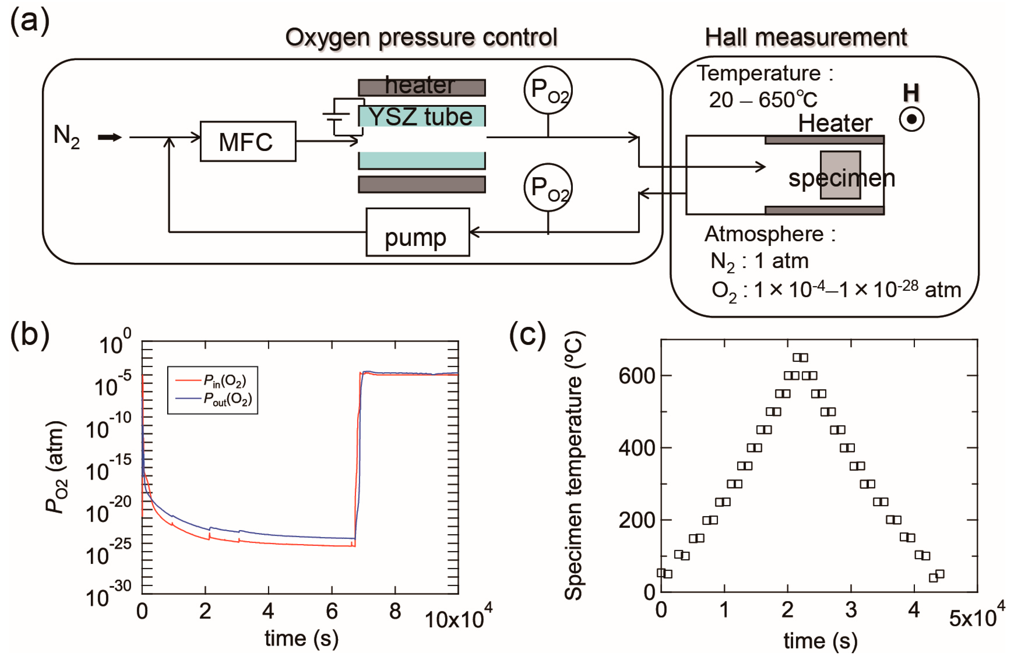
2.2. Properties of ZnO:Al Films Post-Annealed at Low and High Oxygen Partial Pressures
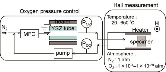
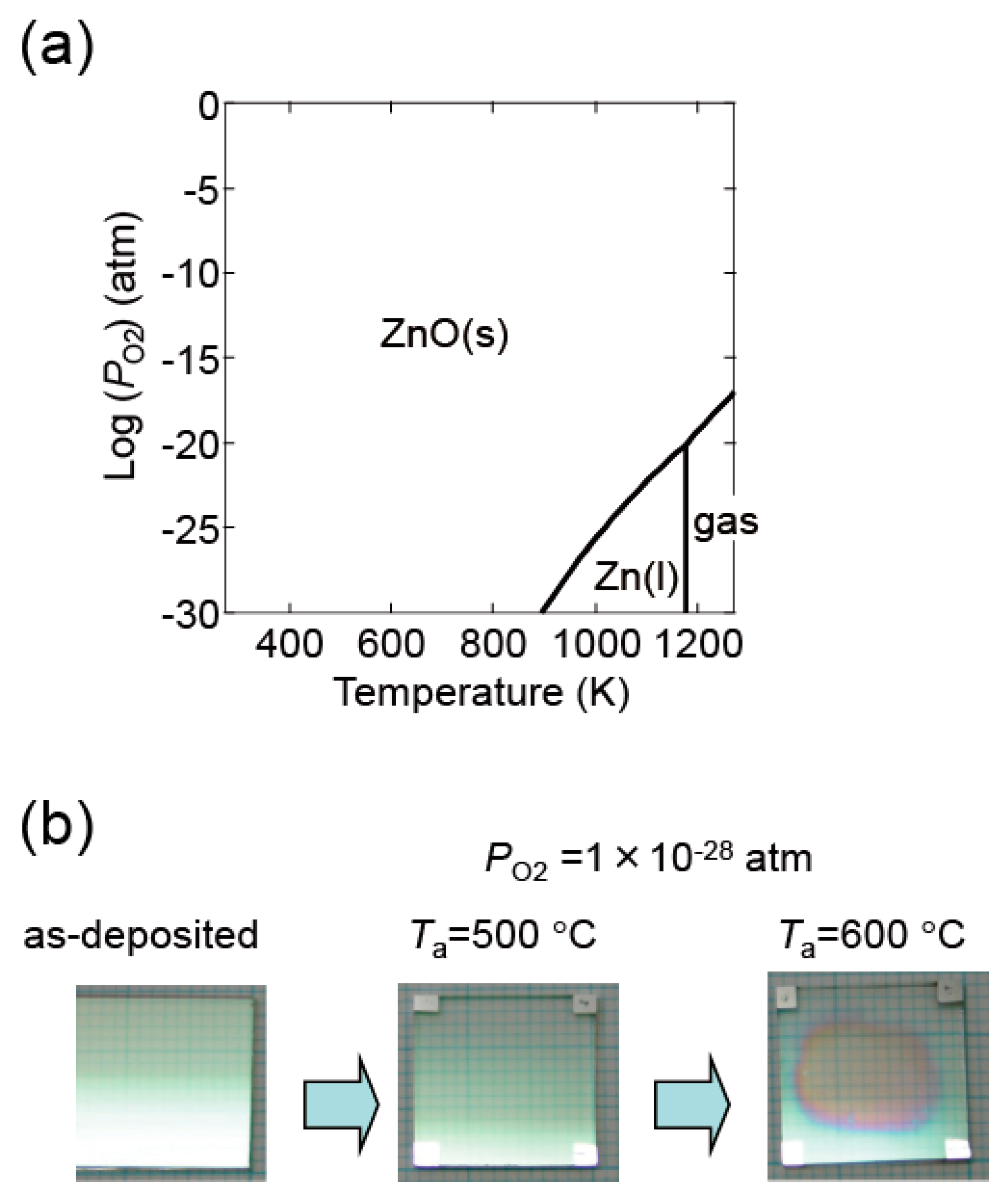
We investigated the effects of post-annealing treatments at low (1 × 10
−23 atm) and high (1 × 10
−4 atm)
PO2 in ZnO:Al (0.25, 0.5, 1.0, 2.0 wt %) films grown at
Topt.
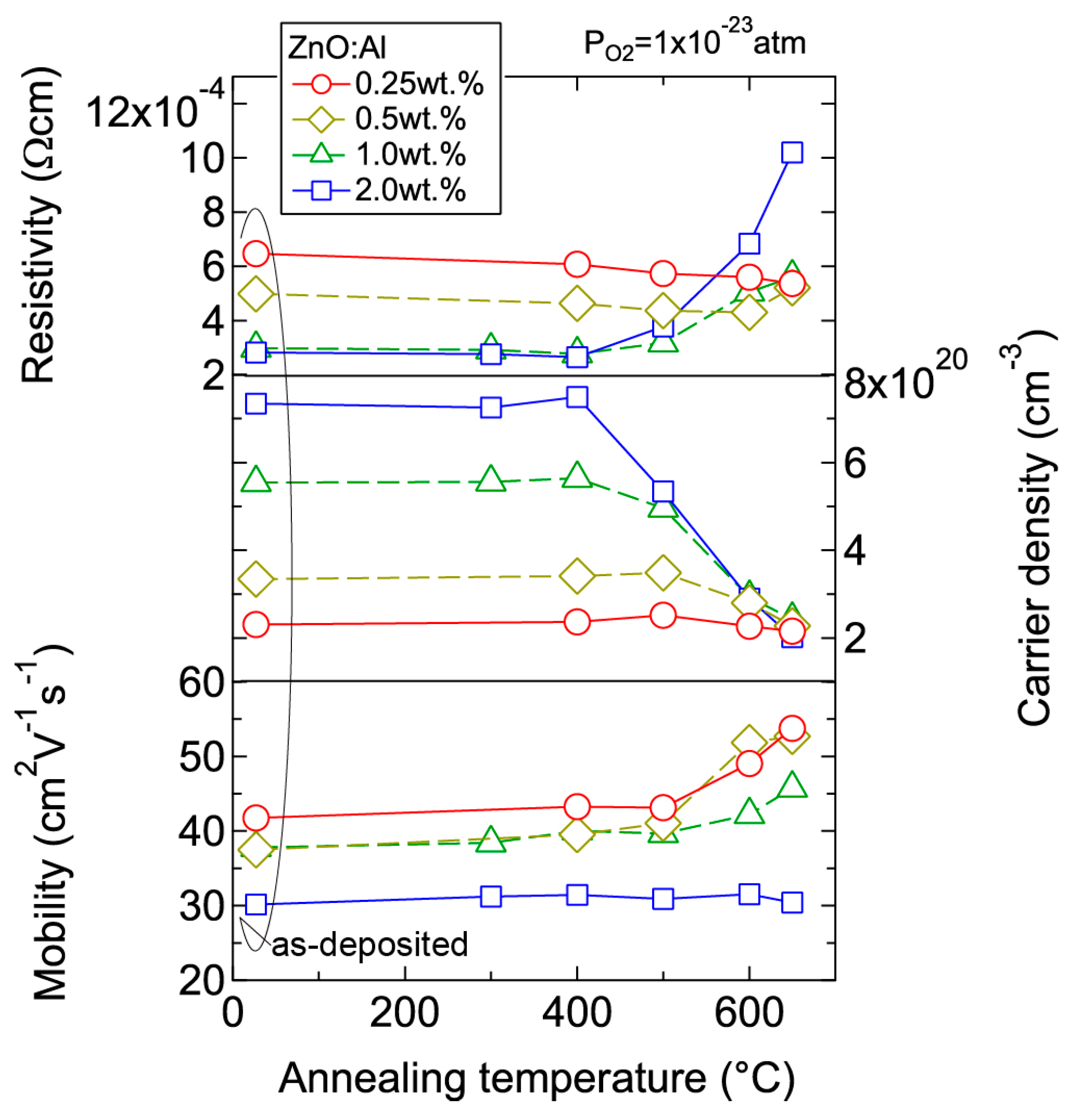
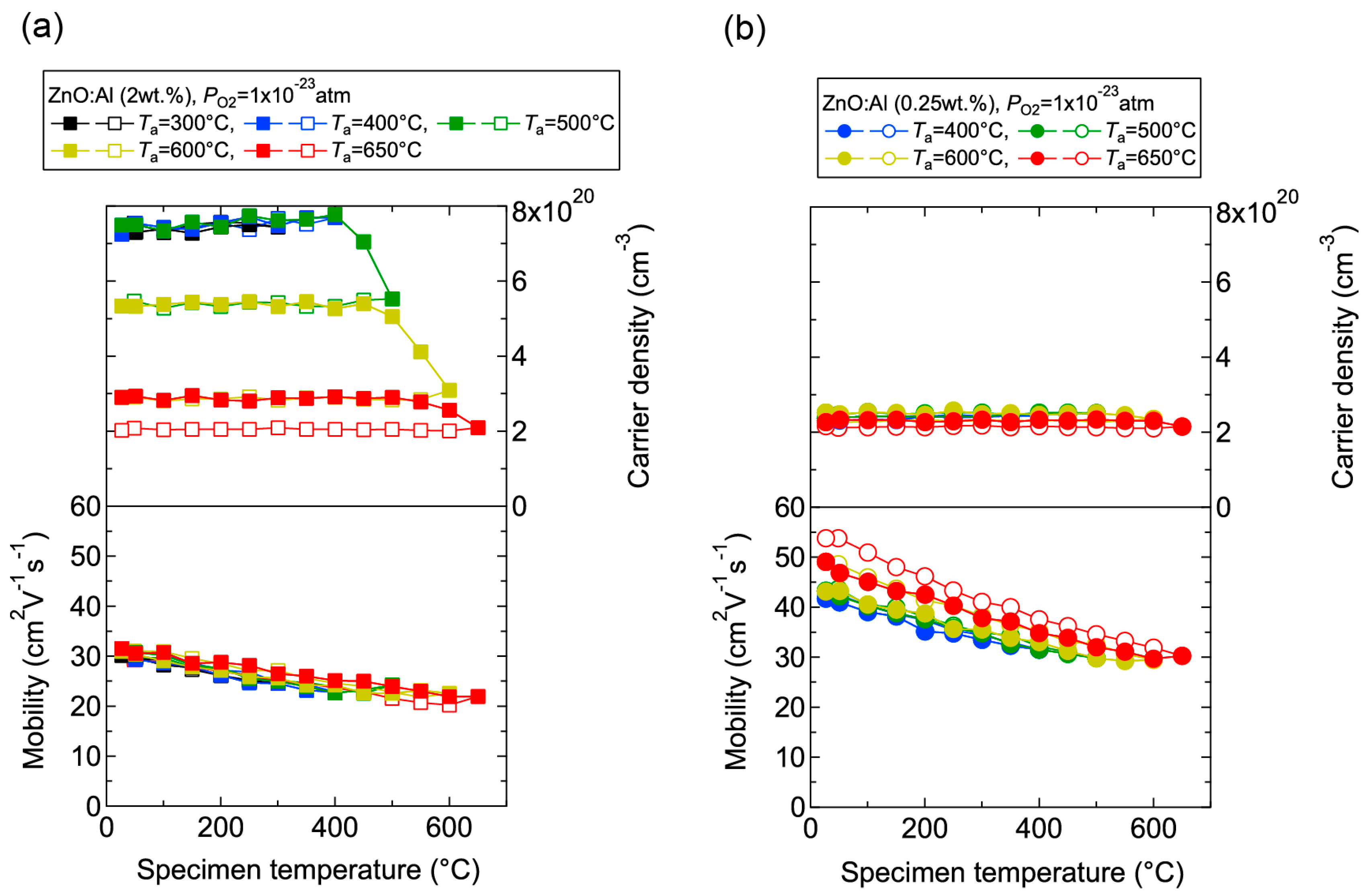
Figure 8 shows the changes in
n and
μ values for ZnO:Al (2.0 wt %) (
Figure 8a) and ZnO:Al (0.25 wt %) (
Figure 8b) films at a
PO2 of 1 × 10
−23 atm as a function of specimen temperature (
Ts) during post-annealing using a Hall measurement system. The measurement system is described in
Section 3. As shown in
Figure 8a, five post-annealing treatments were performed: (i) 50–300–50°C; (ii) 50–400–50 °C; (iii) 50–500–50 °C; (iv) 50–600–50 °C; and (v) 50–650–50 °C. Closed (open) symbols represent data measured during heating (cooling) in each post-annealing treatment. No large changes in
n and
μ were observed up to 400 °C, whereas a large decrease in
n was observed with increasing
Ts above 400 °C. The values of
n during cooling in each annealing treatment were nearly identical to the
n value at the maximum annealing temperature (
Ta). Furthermore, the samples also exhibited similar
n values during heating in each subsequent annealing treatment up to temperatures less than the maximum
Ta in the previous annealing treatment. These results clearly demonstrate that the equilibration time rapidly increases with decreasing
Ts. Therefore, the
n values measured during the cooling process reflect quasi-equilibrium states and frozen defect densities at the maximum
Ta of the annealing treatment. Similar changes in
n values as a function of
Ts were observed for the ZnO:Al (0.25 wt %) film, as shown in
Figure 8b. However, the changes in
n values were very small compared to those of the ZnO:Al (2 wt %) film.
Figure 9 summarizes the changes in
ρ,
n, and
μ values for the ZnO:Al (0.25, 0.5, 1.0, 2.0 wt %) films measured at room temperature after the post-annealing treatments at a
PO2 of 1 × 10
−23 atm. The data are plotted as a function of the maximum
Ta in each annealing treatment. Interestingly, the overall behavior on heating was strongly dependent on the Al content in the films. For the ZnO:Al (0.25 wt %) film,
μ increased from 42 to 54 whereas
n did not change significantly with increasing
Ta. In contrast, for the ZnO:Al (2.0 wt %) film,
n decreased rapidly at
Ta above 400 °C, whereas
μ did not vary at all, as also shown in
Figure 8a,b. Furthermore,
n values began to decrease at lower
Ta values for ZnO:Al films with higher Al contents, resulting in
n values after the high-
Ta annealing treatments that were independent of the Al content: 5.0–5.3 × 10
20 cm
−3 for ZnO:Al (2.0 and 1.0 wt %) films (
Ta = 500 °C), 2.8–2.9 × 10
20 cm
−3 for ZnO:Al (2.0, 1.0, and 0.5 wt %) films (
Ta = 600 °C), and 2.0–2.4 × 10
20 cm
−3 for ZnO:Al (2.0, 1.0, 0.5, and 0.25 wt %) films (
Ta = 650 °C).
The observed changes in
n and
μ were dependent on both
Ta and
PO2.
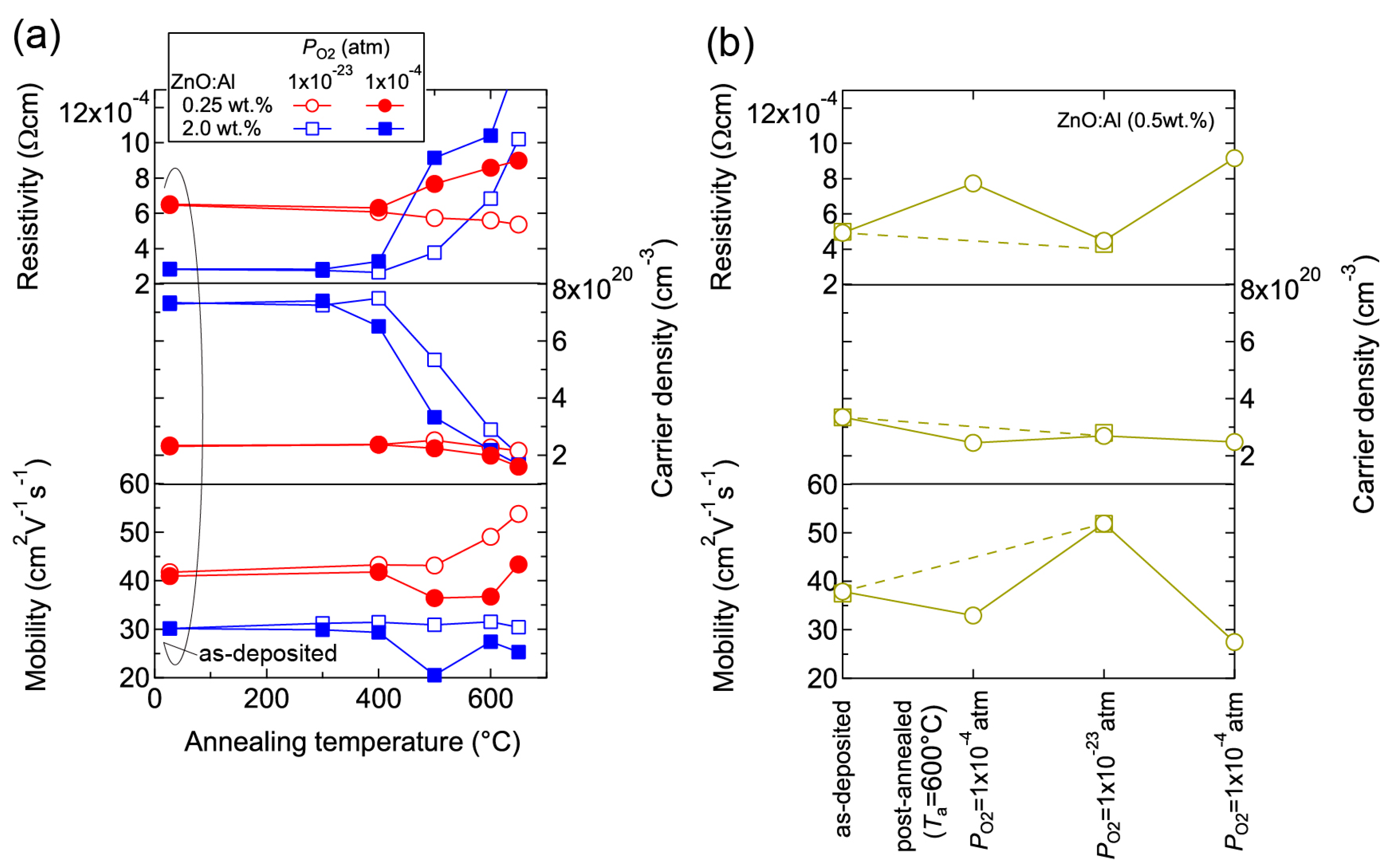
Figure 10 shows room temperature values of
ρ,
n, and
μ for ZnO:Al (0.25 and 2.0 wt %) films plotted as a function of
Ta at
PO2 values of 1 × 10
−23 and 1 × 10
–4 atm (
Figure 10a) and the ZnO:Al (0.5 wt %) films post-annealed at 600 °C at various
PO2 values (
Figure 10b).
Figure 10a indicates that the
μ values for the ZnO:Al (0.25 wt %) film increased only after post-annealing at low
PO2. In addition, the
n values for the ZnO:Al (0.25 and 2.0 wt %) films decreased significantly after annealing at a higher
PO2.
Figure 10b shows the results for two films that were post-annealed at 600 °C at different
PO2 values. One film was annealed at a
PO2 of 1 × 10
−23 atm (dotted lines), while the other film was annealed at a
PO2 of 1 × 10
−4 atm, followed by an annealing treatment at a
PO2 of 1 × 10
−23 atm and a subsequent annealing treatment at a
PO2 of 1 × 10
−4 atm (solid lines). Both films exhibited similar transport properties after the annealing treatments at the same
PO2 (1 × 10
−23 or 1 × 10
−4 atm), thereby reflecting their thermodynamic quasi-equilibrium states.
To elucidate the origin of the changes in
n and
μ, we characterized the structural properties of the films using TEM and XRD, and the chemical properties using X-ray photoelectron spectroscopy (XPS) and thermal desorption spectroscopy (TDS).
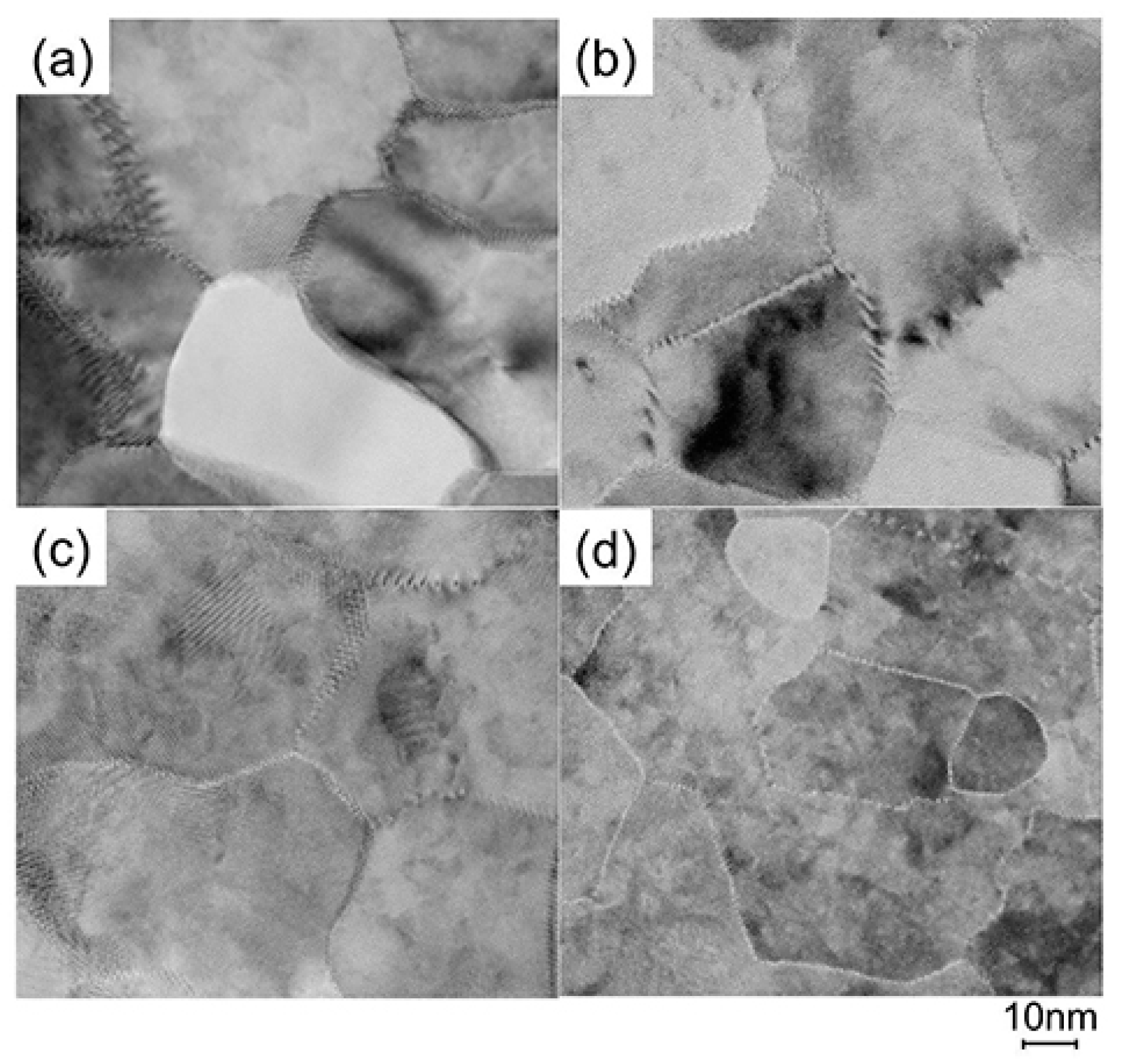
Figure 11 displays plan-view TEM images of the as-deposited and post-annealed ZnO:Al (0.25 and 2.0 wt %) films at 650 °C. Most grain boundaries observed in the films were [001] tilt-type boundaries with a [001] rotation angle. This is because both films exhibited
c-axis preferred orientations, as indicated by the FWHM
ω002 of ca. 2°–3° (
Figure 3).
Figure 11a,b clearly shows that both of the as-deposited films contained strained regions that propagated toward the grain interior from the GBs. The strained regions are assumed to have been produced by unavoidable orientation mismatches between adjacent columns during crystal growth. After the post-annealing treatment, many of the boundaries appeared flat and located parallel to the
c-axis at least within a thickness of the TEM foil for both films (
Figure 11c,d). This feature may be attributed to grain growth that reduces the grain boundary area to achieving energetically favorable boundaries. Indeed, the FWHM
100 slightly decreased with
Ta.
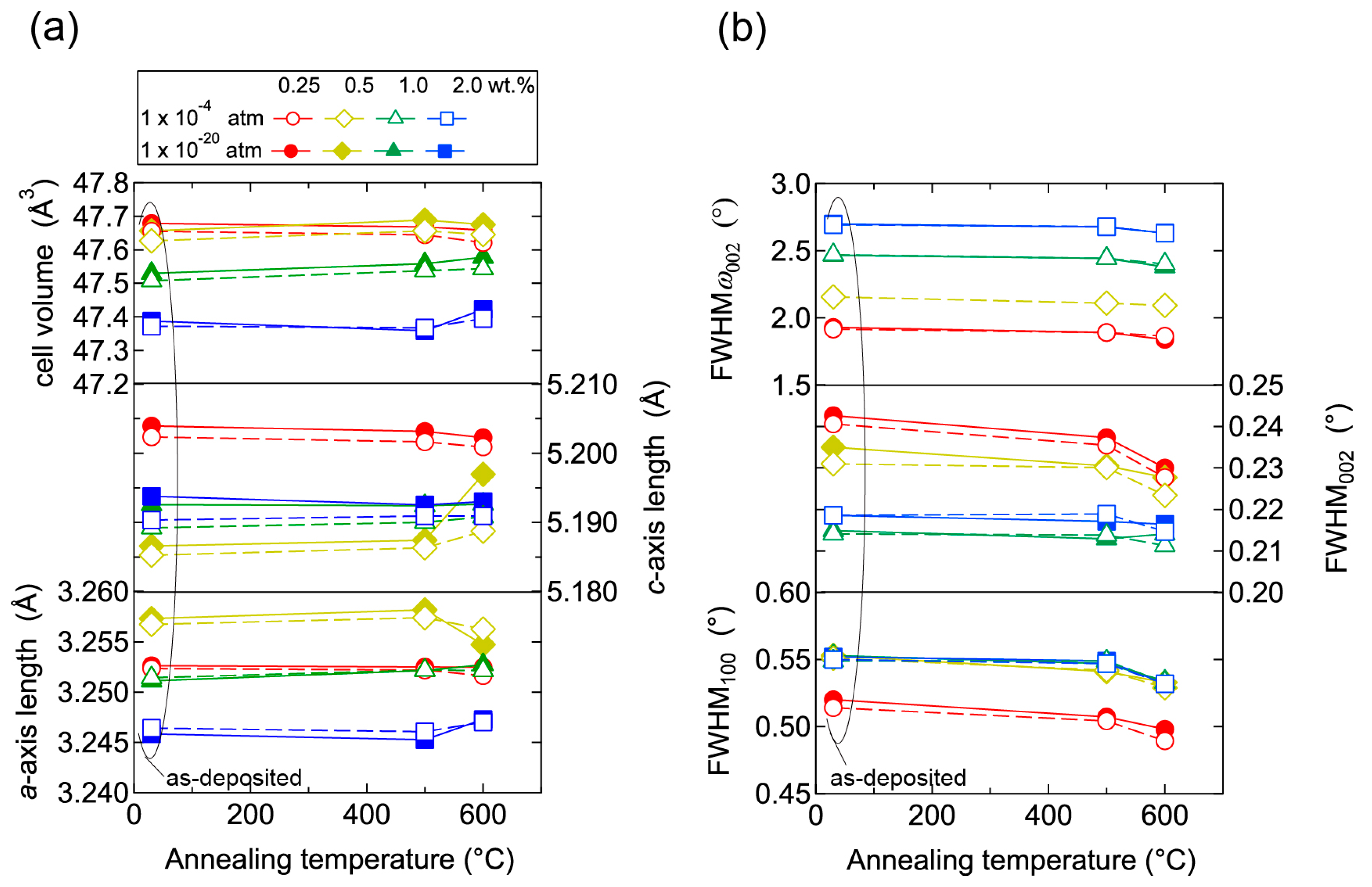
Figure 12 shows the
a- and
c-axis lengths and cell volume (
Figure 12a) along with FWHM
ω002, FWHM
002, and FWHM
100 (
Figure 12b) for the post-annealed films at
PO2 values of 1 × 10
−20 and 1 × 10
−4 atm as a function of
Ta. These values were strongly dependent on the Al content as a result of the strong influence of
Tg and thickness on the structural properties, as discussed in
Section 2.1.
Figure 12b shows that the FWHM
002 and FWHM
100 decreased with
Ta above 500 °C, with the same changes observed at both low and high
PO2. Furthermore, no significant differences in the other measured values were detected between the films post-annealed at low and high
PO2. In contrast, the
μ and
n values shown in
Figure 10 strongly depended on
PO2. Therefore, the decrease in the strained region around the GBs and a slight increase in the in-plane crystallite size indicated in
Figure 11 and
Figure 12 were not responsible for the increase in
μ. Additionally, the different
n values produced by post-annealing at different
PO2 values are not due to changes in the structural properties observed by TEM and XRD analysis.
Conversely, high-temperature annealing at low
PO2 is likely to change the chemical properties of the films.
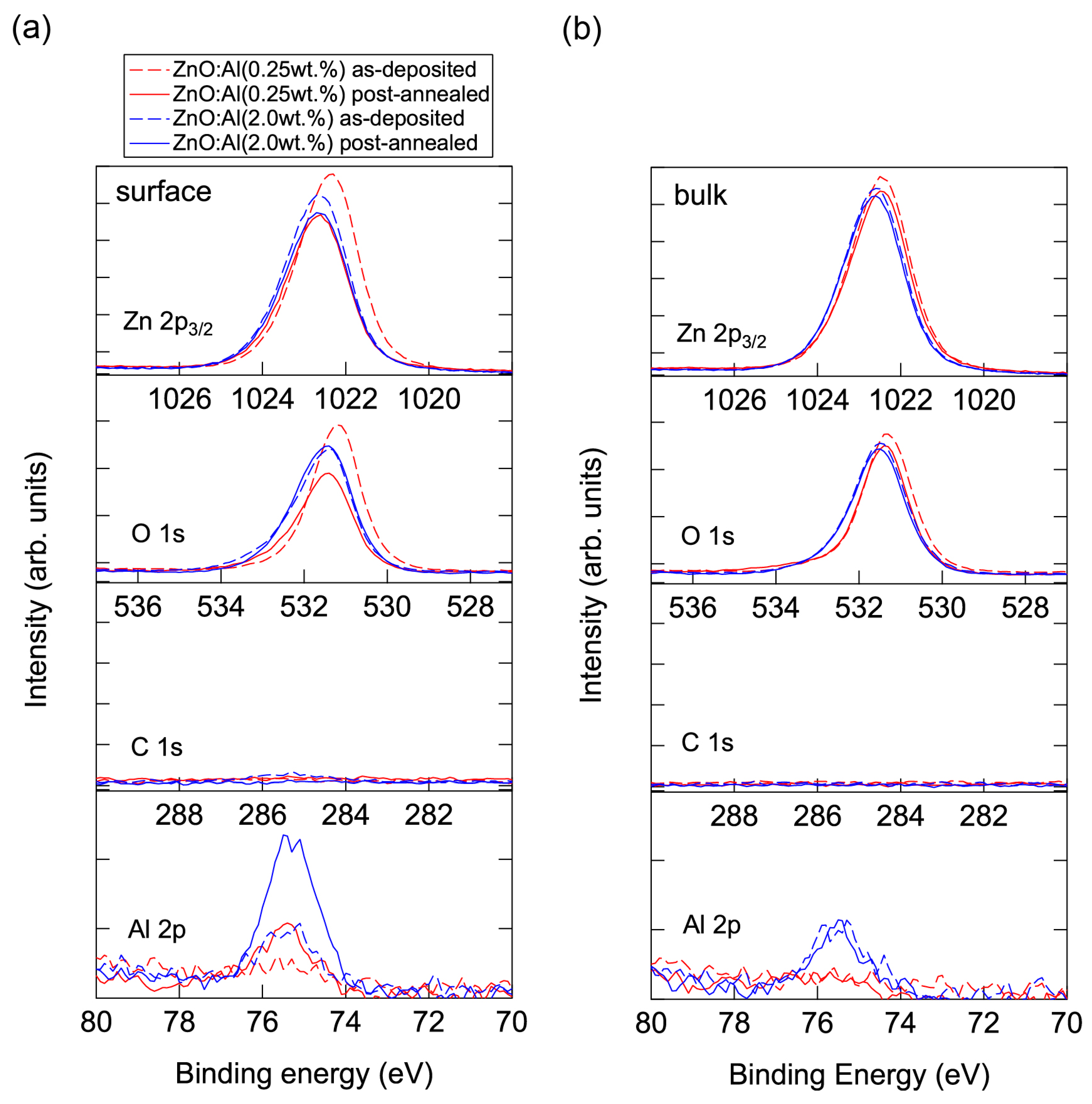
Figure 13 shows XPS spectra for the surface regions (
Figure 13a) and bulk regions (
Figure 13b) of the as-deposited and post-annealed ZnO:Al films.
Figure 13a indicates that the Al contents in the surface regions were significantly higher than in the bulk films for both post-annealed ZnO:Al (0.25 and 2.0 wt %) films. The concentrations of Al, Zn, and O (
CAl (at %),
CZn (at %), and
CO (at %)) estimated from the XPS spectra are summarized in
Table 1. The results suggest that minor decomposition of the ZnO layer occurs in the surface region during high-temperature annealing at low
PO2. This is also supported by the TDS spectra for the ZnO:Al films.
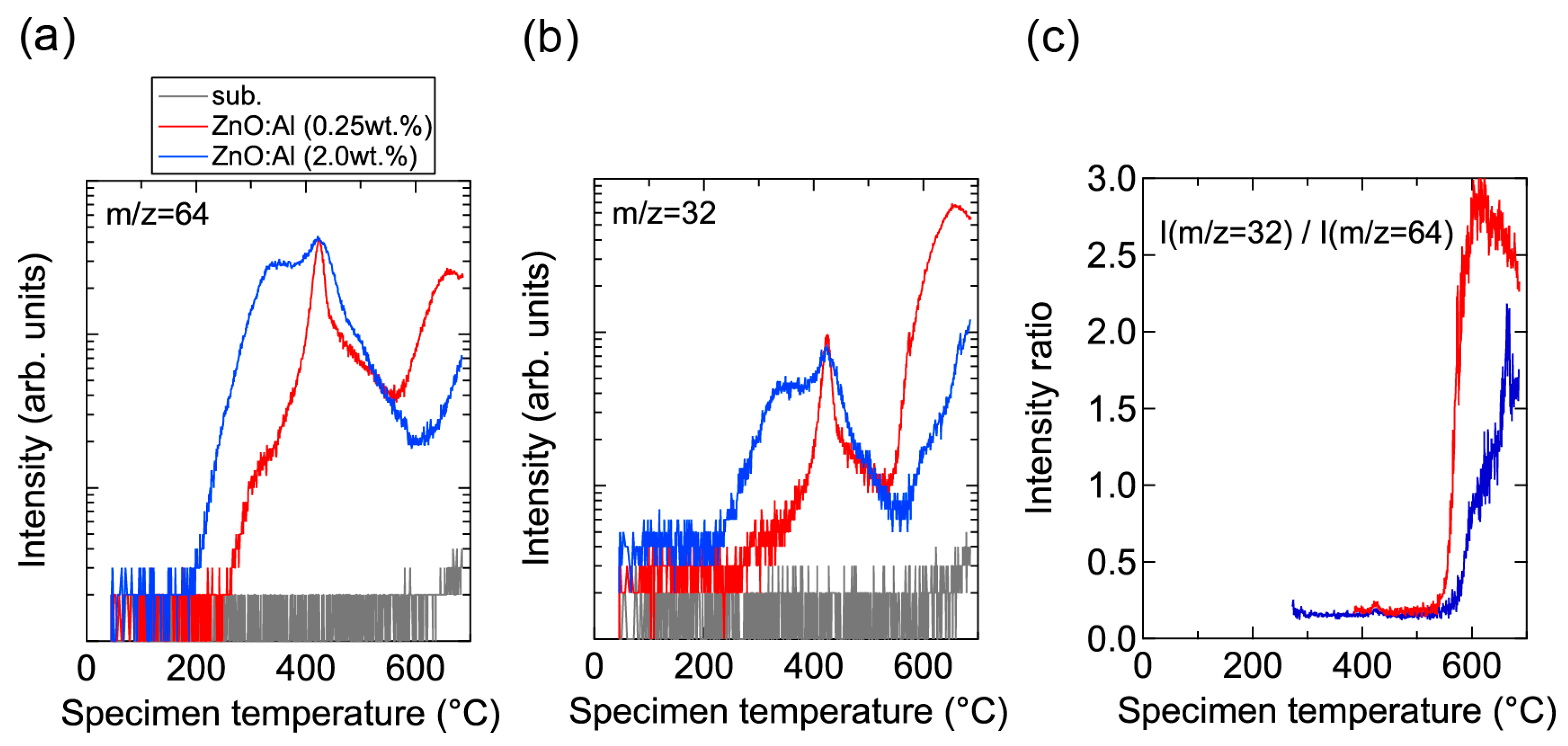
Figure 14 shows the TDS spectra of desorption species from the ZnO:Al (0.25 wt %) and ZnO:Al (2.0 wt %) films grown at
Topt. We monitored the mass (m/z) of (a) 64; (b) 32; and (c) the ratio between the two. Here, an m/z value of 64 includes only Zn
+, whereas an m/z of 32 includes both Zn
2+ and O
2+. The behavior of the m/z = 32 signals were similar to those of the m/z = 64 signals with a constant ratio, especially for
Ts below 530 °C, thereby indicating that most of the m/z = 32 signals below 530 °C reflect the desorption of Zn rather than O
2. In contrast, at temperatures above 530 °C, the m/z = 32 signals sharply increased with
Ts and exceeded the level of the m/z = 64 signals, thereby indicating that O
2 was also desorbed. Hence, decomposition of the films began at
Ts values above 500 °C in a high vacuum (i.e., <1 × 10
−7 Pa).
Prior to the onset of decomposition, defects within grains are likely to change during the post-annealing treatment at high temperatures and at low
PO2. As observed in
Figure 14a, Zn became desorbed from the surface of the films at temperatures above ~200 °C. Furthermore, a larger amount of Zn was desorbed from the ZnO:Al (2.0 wt %) film compared to the ZnO:Al (0.25 wt %) film. Although the desorption behavior was complex, the signals exhibited peaks at ~350 °C and ~430 °C with a shoulder at ~470 °C in both films. These behaviors are considered to reflect changes in Zn-related defects in the ZnO:Al films. During post-annealing, Zn interstitials diffused from the bulk layers, especially along GBs, and became desorbed from the film surface. A potential source of the Zn interstitial is excess Zn inside the films. Another candidate is Zn interstitials that were generated by the removal of Zn from the ZnO lattice along with the generation of Zn vacancy during the post-annealing treatment, with acceptor-type Zn vacancy remaining inside the grains. First-principle density functional theory suggests that acceptor-type v
Zn″ defects are formed and that carrier compensation occurs in ZnO:Al with increasing
PO2 [
4,
5,
6,
7]. The density of v
Zn″ increases with Al content in ZnO:Al because the formation energy of v
Zn″ decreases with increases in the Fermi energy of ZnO. In addition, Zn
i•• can diffuse even through the bulk lattice due to a low migration barrier [
7]. Based on the combination of these theoretical suggestions, a decrease in
n at temperatures above 400 °C—especially for heavily Al-doped ZnO films at high
PO2 (
Figure 9 and
Figure 10), desorption of Zn at these temperatures (~430 °C) under a high vacuum (i.e., <1 × 10
−7 Pa) (
Figure 14a), and no presence of Zn vapor during the post-annealing processes under the constant
PO2—Zn interstitials and Zn vacancies are thought to be created in the ZnO lattice during post-annealing at temperatures above 400 °C. Therefore, Zn desorption from the films and carrier compensation by acceptor-type v
Zn″ occurred simultaneously. In contrast, desorption of Zn below 400 °C had no influence on the
n values, as observed in
Figure 8,
Figure 9, and
Figure 14. The results suggest that excess Zn that does not contribute to carrier generation is present within the as-deposited films. Although the formation energy of a Zn
i•• is high, and thus high densities of Zn
i•• are not expected in ZnO at equilibrium conditions [
4,
6,
7], a large amount of Zn may be introduced into the films grown using a non-equilibrium growth method, especially when grown under Zn-rich conditions at low temperatures. Indeed, several papers have also reported the detection of Zn desorption from sputtered ZnO films in TDS spectra for films grown under low O
2/Ar flow ratios [
19,
20,
21,
22]. It should be noted that Zn desorption decreases with increasing O
2 desorption at high O
2/Ar flow ratios [
22]. In addition, we observed a monotonic decrease in
n with increases in the O
2/(Ar + O
2) flow ratio: 1.7 × 10
20, 3.1 × 10
20, 5.1 × 10
20, and 5.4 × 10
20 cm
−3 for ZnO:Al films grown at a ratio of 1%, compares with 1.4 × 10
20, 2.3 × 10
20, 4.3 × 10
20, and 3.8 × 10
20 cm
−3 for ZnO:Al films grown at a ratio of 2% with Al
2O
3 contents of 0.25, 0.5, 1.0, and 2.0 wt %, respectively. These results suggest that thin-film growth during sputtering without the introduction of O
2 produces Zn–rich conditions. Such conditions will prevent the generation of large amounts of v
Zn″ during growth and heavy carrier compensation by the v
Zn″.
The large increase in
μ after low-
PO2 annealing for ZnO:Al films with low Al contents can be explained by a reduction in scattering centers at GBs. As described in
Section 2.1,
μ for the ZnO:Al films is influenced by GB scattering in addition to scattering from ionized impurities.
Figure 10b illustrates that
μ increased after low-
PO2 annealing, whereas
μ decreased after high-
PO2 annealing. As shown in
Figure 12, no notable change in the structural properties was observed between the films post-annealed at low and high
PO2. In contrast, we detected a change in the chemical states of the film surfaces by XPS and TDS measurements in films post-annealed at low
PO2. These results suggest that point defects at GBs that act as scattering centers are reduced by low-
PO2 annealing. Conversely, we did not observe any increase in
μ in a post-annealed ZnO:Al (2.0 wt %) film with a similar
n value, likely due to an increase in the compensation ratio by the generation of large amount of v
Zn″, as discussed above.
Based on these results, carrier compensation occurs by the generation of v
Zn″acceptor-type defects when sputtered ZnO:Al films are post-annealed at high temperatures. The compensation behavior differs with Al content. For high-Al ZnO:Al films (i.e., 2.0 wt %),
n starts to decrease at ~400 °C even at a low
PO2 of 1 × 10
−23 atm, whereas in low-Al films (i.e., 0.25 wt %),
n starts to decrease at ~600 °C. Furthermore, the amount of desorbed Zn and the amount of acceptor-type defects estimated from the changes in
n values increase with Al content. These results are in good agreement with theoretical predictions [
6]. Practical applications require higher
n and
μ values. Low-
PO2 annealing is effective in increasing
μ values, likely due to reduction in the amount of point defects at GBs that act as scattering centers. However, at present,
n values are small compared to the Al content and a portion of the free carriers is likely to be trapped by crystal imperfections, as described in
Section 2.1. In this case, controlling the presence of tilt-type GBs in Zn-rich conditions will be important [
23]. Additionally, Zn vacancies and other related defects have been detected in as-deposited ZnO films by positron annihilation [
24,
25]. Self-compensation by the production of v
Zn″ has also been experimentally demonstrated for as-deposited Ga-doped ZnO films [
10]. Therefore, passivation of the existing v
Zn″ defects by a post-annealing treatment can be useful. For example, post-annealing in a Zn atmosphere is a candidate method for reducing v
Zn″ concentrations. Experimental studies have also reported that post-annealing treatments in a Zn atmosphere improve both
n and
μ values [
26,
27]. Also, hydrogen has been proposed to passivate acceptor-type cation vacancies [
28]. Other experiments have also found that annealing treatments in forming gas (5%–10% H
2/balance Ar or N
2) [
10,
27,
29] and hydrogen diffusion from SiN
x:H or a-Si:H layers [
30,
31] can improve both
n and
μ values.


