2. Theory and Model Specifications
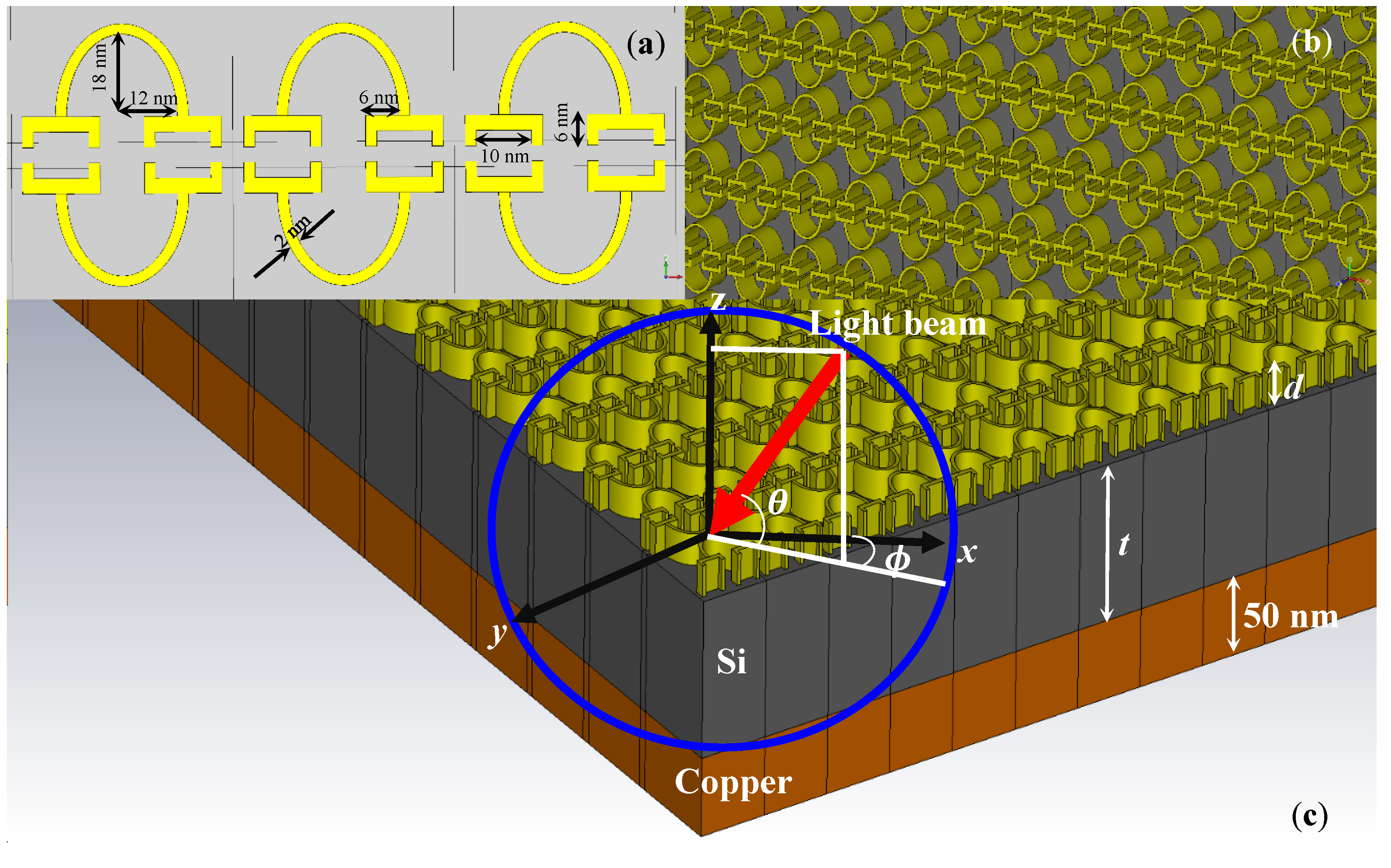
The metamaterial nanostructure includes two main butt-facing U-shapes of nanoscaled gold structure, which are inversely positioned up-facing towards each other. Combination of both the U-shapes serves as only a one unit cell, as shown in
Figure 1a. However, the curvature of U-shape is closely similar to a circular ring, and symmetrical parabolic shapes having 2 nm width perform as a ring. The total dimension of butt-facing U-shape within the unit cell is much smaller than the excitation wavelength—this remains of great importance since the plasma frequency is related to the electron density of metasurface within the MPA structure through the equation [
16],
where
,
and
and
represent electron density, electronic mass, electronic charge and free-space permittivity, respectively. The light beam, which is the external EM field, causes free-electrons (plasma) to oscillate towards the direction in which it is applied. These free-electrons, confined inside the U-shaped nanostructure, move in the
-direction as the incident light impinges from the
-direction. As a result, the whole metamaterial structure would not take part in the movement of charge.
The effective electron density
, developed due to the fraction of free-electrons participating in resonance (due to the effect of external incident light beam), is directly related to the size and the effective mass of the butt-facing U-shaped structure within each unit cell, and inversely related to the distance between neighboring U-shapes. Thus, the effective electron density of U-shape due to asymmetrical properties (of the structure) is mainly related to the distance of separation between the up- and the down-vertex points of each U-shape. Moreover, the width of the U-shape also plays an important role in enhancing the effective electron density of the structure. Generally,
can be expressed as:
where
is the size of the up- and the down-shaped U-shape, and
is the effective distance between two U-shapes.
Figure 1a shows dimensional features of the metamaterial structure within the unit cell that constitutes the top metasurface (as illustrated in
Figure 1b). The values of the thickness
of (the gold) metasurface are taken as typically 50 nm and 100 nm. The case of
will essentially yield a simple metal loaded planar guide configuration—this situation is also considered in this paper, in order to compare the results. Further, small values of
would contribute to the generation of surface plasmonic waves, the effects of which are primarily discussed in the present work.
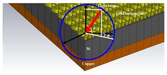
Figure 1c shows the schematic of MPA that incorporates the lower layers as Si and copper. The Si layer thickness
is typically chosen as 100 nm and 500 nm, in order to evaluate the effect on the absorption characteristics due to the variation in thickness of the wave confinement section; the (lowest) copper layer thickness remains fixed at 50 nm. It is noteworthy that the Si and the copper layers perform as the light trapper and prefect light reflector, respectively.
The spherical coordinate in
Figure 1c is purposely illustrated to feature the trace of the incoming light beam along with the
-direction. The importance of it lies in that the metasurface is essentially an anisotropic medium, and the spectral behavior (of MPA) is analyzed when the incident angle
sweeps a wide range under transverse electric (TE) and transverse magnetic (TM) polarizations (of the incidence excitation). Also, in some cases, the results are obtained corresponding to the two different values of the azimuthal angle
(viz.
and
), in order to illustrate the effect of
on the absorption characteristics. The scattering matrix, developed by the CST simulator, is used to analyze the frequency-dependent absorption of the MPA structure; the detector is essentially considered as placed below the copper nanolayer.
3. Results and Discussion
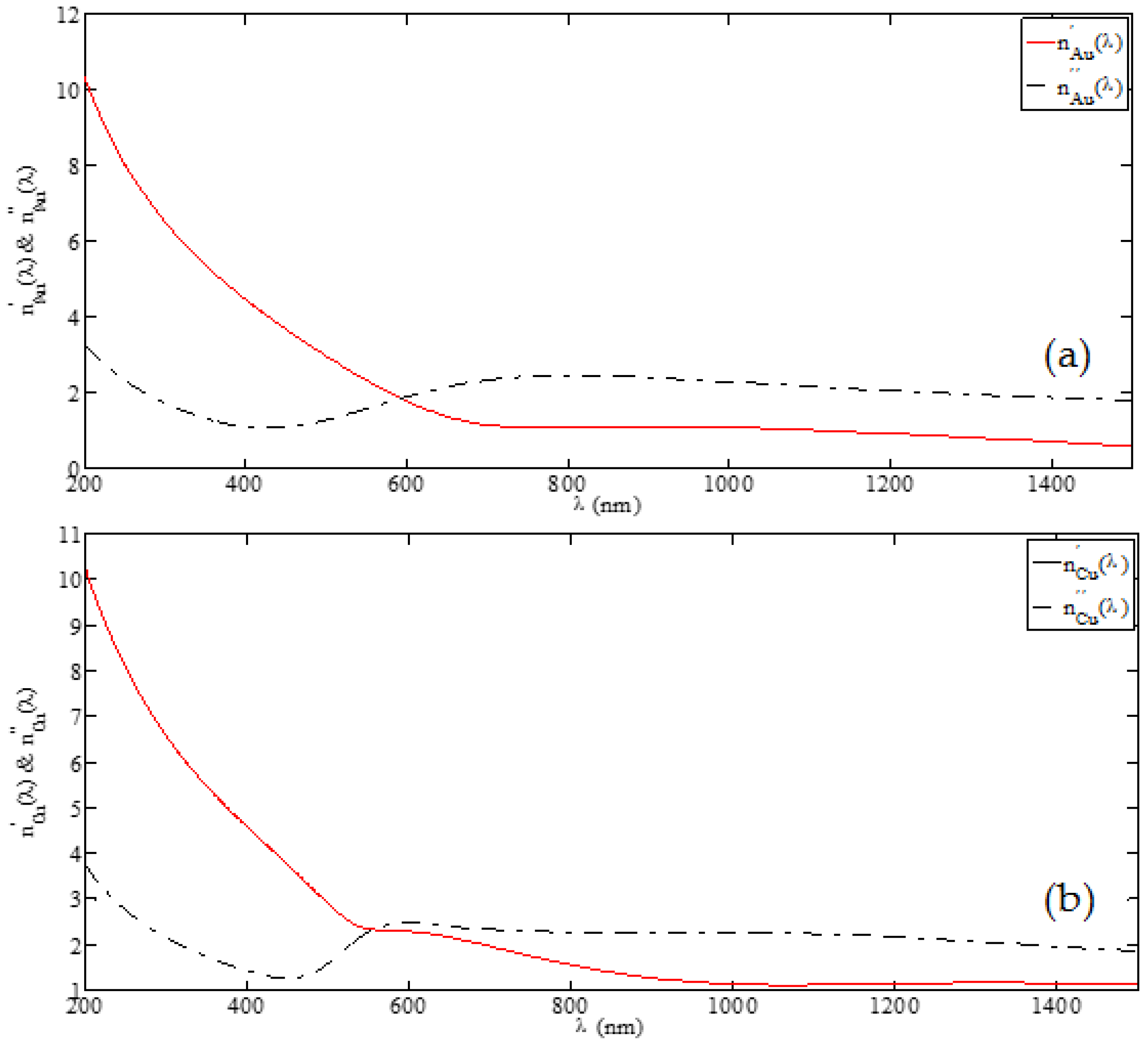
Figure 2 illustrates the refractive index (
RI) dependence of gold and copper on the wavelength
in the NUV and NIR regions (200–1500 nm) of the EM spectrum. Since the
RI values remain complex in nature, we represent those in the cases of gold (Au) and copper (Cu) as
and
, respectively. Further the
RI value of Si is taken as
. It is clear from
Figure 2 that gold and copper both exhibit decrease in
RI with increasing wavelength, and for higher wavelengths, the
RI values become almost independent (of wavelength). Also, the imaginary part of
RI remains larger for higher wavelengths.
Figure 3 and
Figure 4 illustrate absorption patterns for the MPA structure under consideration. In these plots, the behavioral features of the absorption coefficient
are shown against the wavelength
in the NUV and NIR regions (as described above) corresponding to the different incident angles
(keeping the azimuthal angle as
), metasurface thickness
, Si layer thickness
and the polarization states of the incident light (
i.e., TE or TM). The angle of incidence is varied from
to
in a step of
. The incident angles below
and above
yield absorption characteristics in the lower and the higher spectral bands, wherein alterations have been observed to be less significant as compared to those obtained for the angular range between
and
, and therefore, those portions of absorption spectra are not taken into account. It must be noted down at this point that the EM waves are generally allowed to sweep across the target with various angles of incidence
, and therefore, the azimuthal angle
is kept fixed to
in this case.
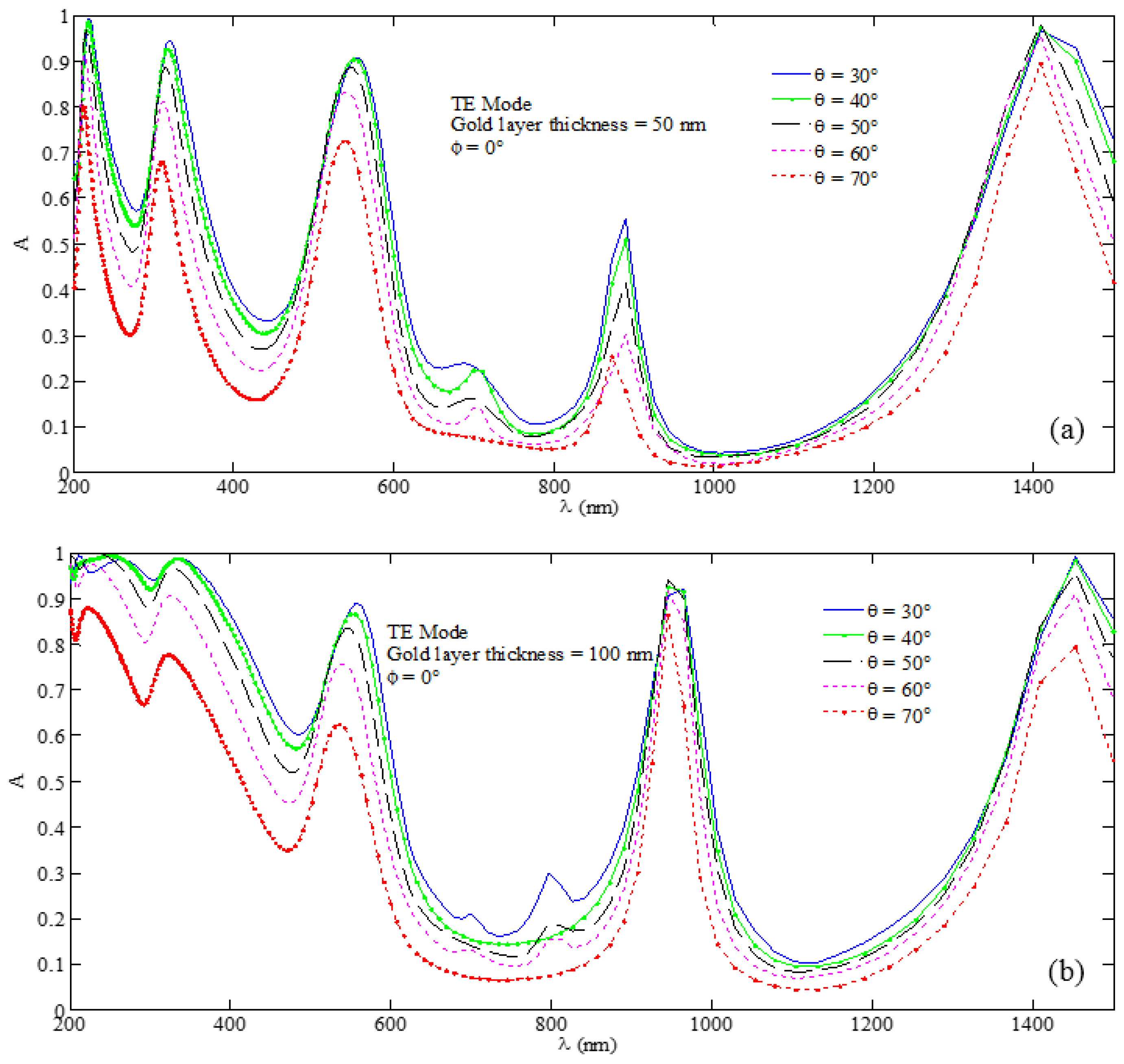
Figure 3a shows absorption spectra under the TE polarization state of incident light when the thickness
of the metasurface is 50 nm. It can be observed that, among the other peaks at different wavelengths, the MPA structure exhibits the highest absorptivity
) at the angle
corresponding to the wavelength
219.08 nm. The first plasmonic peak appears between 200 and 325 nm, and the lowest peak in this range appears corresponding to
at the wavelength
212 nm. The increase in incidence angle form
to
causes small blue-shifts in the absorption peak. The second and the third plasmonic peaks, that yield more than 96% absorption, appear in the visible regime with wavelength spans
309.0–319.76 nm and
536.3–555.8 nm, respectively. This briefly shows that the angle of incidence of the incoming wave would effectively lead to wider blue-shift at the upper band of the NUV class.
Besides these,
Figure 3a depicts that there are two more peaks located at the lower and the upper bands of the NIR class. The first peak is less significant owing to low absorptivity (which is less than 60%) at
nm, but the second peak at
nm possesses different characteristics, as compared to the rest of the peaks. It can be clearly noticed from
Figure 3a that the MPA shows very high absorptivity (
) corresponding to
, as compared to the other values of incident angles. More importantly, the effect of blue-shifts in absorption spectra almost vanishes for all incidence angles when the absorption peaks remain centered at
nm with the absorptivity value as
.
Results corresponding to the TE wave incidence excitation for
nm show different absorptivity conditions (
Figure 3b). This case clearly indicates that the wavelength range
200–370 nm is considerable since, at the incidence angles
and
, absorptivity remains above 90%. Further, the absorption peaks in this range are not enough sharp; the maximum sharpness is achieved near
nm. In
Figure 3b, the actual plasmonic peaks in the visible range appear in the wavelength span
539–555 nm, and similar to the situation for
nm, the highest absorption peak appears at
nm corresponding to
incidence.
The most important feature of spectral behavior corresponding to the TE-polarized incident wave is that, while using the metamaterial thickness
nm, the absorption peaks are weak in terms of sharpness, whereas the choice of
nm makes the peaks strongly magnified and centered at
nm. In
Figure 3b as well, the blue-shifts in absorption peak, as a result of variation in incidence angle, remain strongly obvious. In this figure, the peak amplitude of absorption corresponding to
and
nm is almost 92%, whereas for
and
nm, it is nearly 86%. This clearly indicates a shift of
20 nm due to the
rotation of incidence angle of the wave.
The last set of peaks in
Figure 3b, in contrast to the case of
nm (
Figure 3a), indicates that
is the incidence angle where the highest peak (with 99.1% absorption) appears at
nm. Further, similar to the case of
Figure 3a, the choice of
nm eliminates blue-shifts of plasmonic peaks in the wavelength range in the vicinity of
nm.
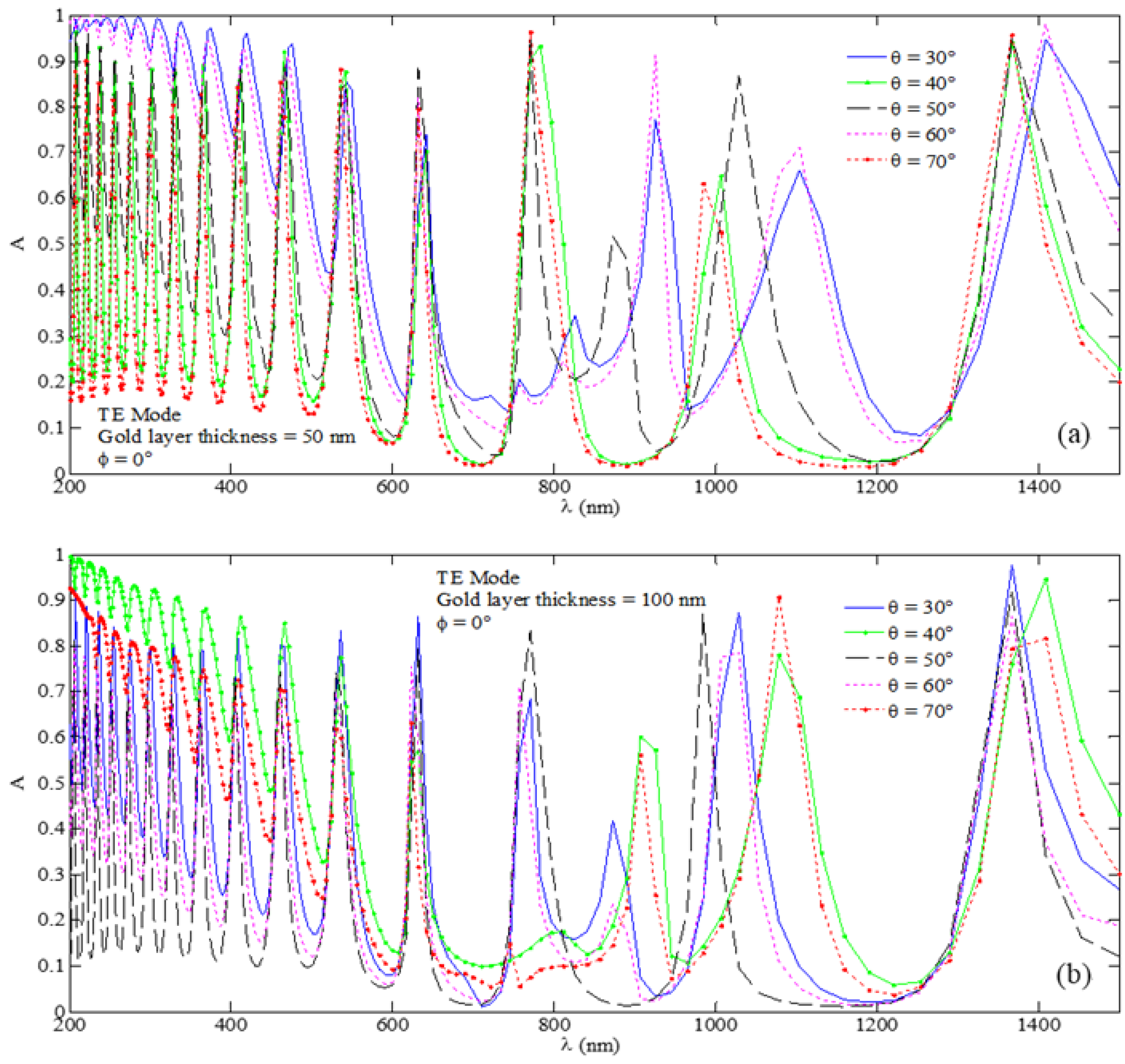
In order to see the effect of the Si layer, the thickness
(of this region) is increased to 500 nm, and the absorption spectra are shown in
Figure 4. Comparing the results with those obtained with the 100 nm thick Si layer (
Figure 3), it can be observed that the number of absorption peaks is now significantly enhanced, and the structure behaves as comb filter [
14]. The reason for this is very obvious: the enlarged thickness of wave trapping section will essentially allow proliferation of modes, thereby causing the existence of more absorption peaks. A comparative look at
Figure 4a,b leaves impression that the increase of metasurface thickness results in a little more absorption peaks—the feature that has been observed to some extent in
Figure 4 too, corresponding to the case of 100 nm Si layer thickness. However, it is the combinational effect of both the metasurface thickness and the wave confinement section thickness that ultimately enhances (or manipulates) absorption peaks of the MPA. This is further justified from
Figure 4 which demonstrates over 99% absorption in the short wavelength span with 50 nm metasurface thickness.
The cases discussed in
Figure 3 and
Figure 4 correspond to the situation when the azimuthal angle
assumes
value. As the metasurface is anisotropic in nature, it would be interesting to observe the effect of
on the absorption characteristics.
Figure 5 illustrates the case when the TE wave incidence happens with
; the sweeping values of the angle
are taken similarly as in the afore-discussed situations. Further, we choose the illustrative cases of metasurface layer thickness
nm (
Figure 5a) and
nm (
Figure 5b), keeping the Si layer thickness fixed to
nm.
We observe in
Figure 5 that, in both the situations, the patterns of absorption features are significantly altered, and the positions of absorption peaks are less prominently defined, as compared to that in
Figure 3. This happened in the entire range of wavelength under consideration. As such, the choice of
may not be that appropriate for the usage of the metasurface-based device for the absorber kinds of applications.
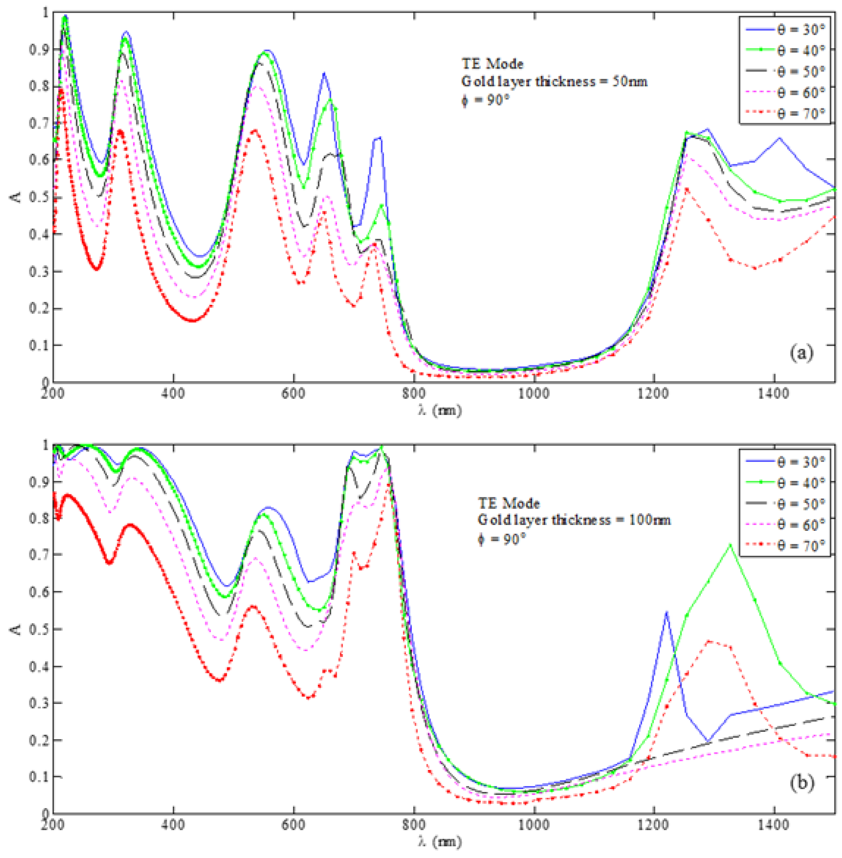
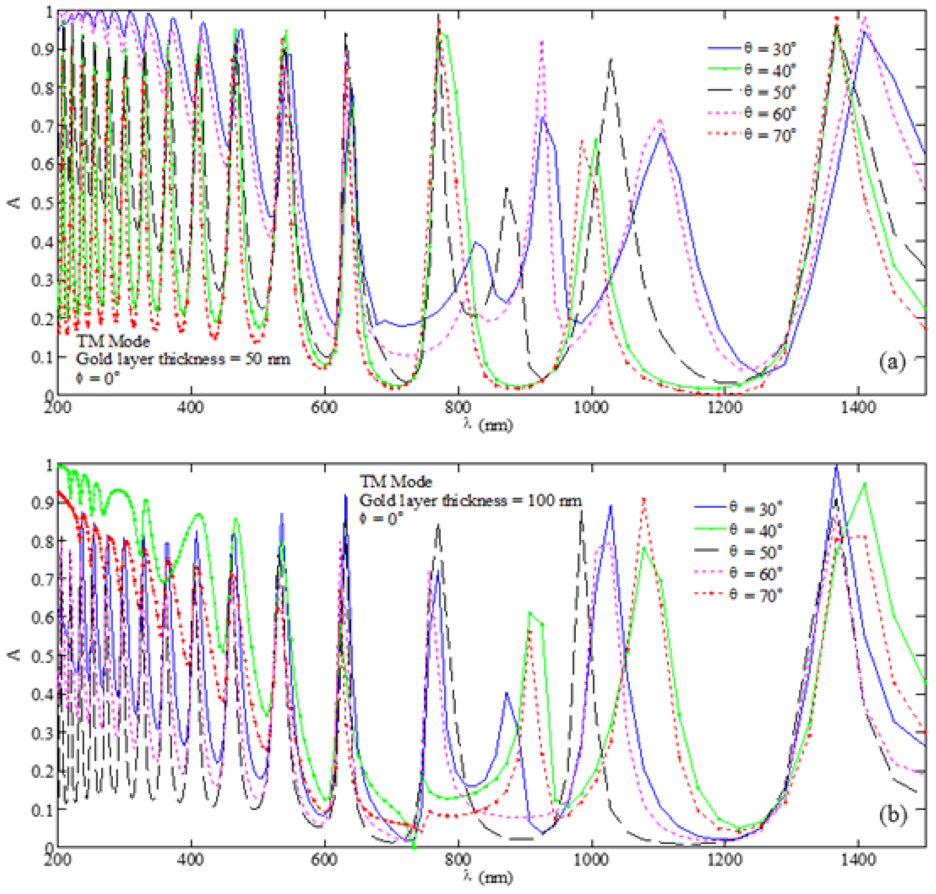
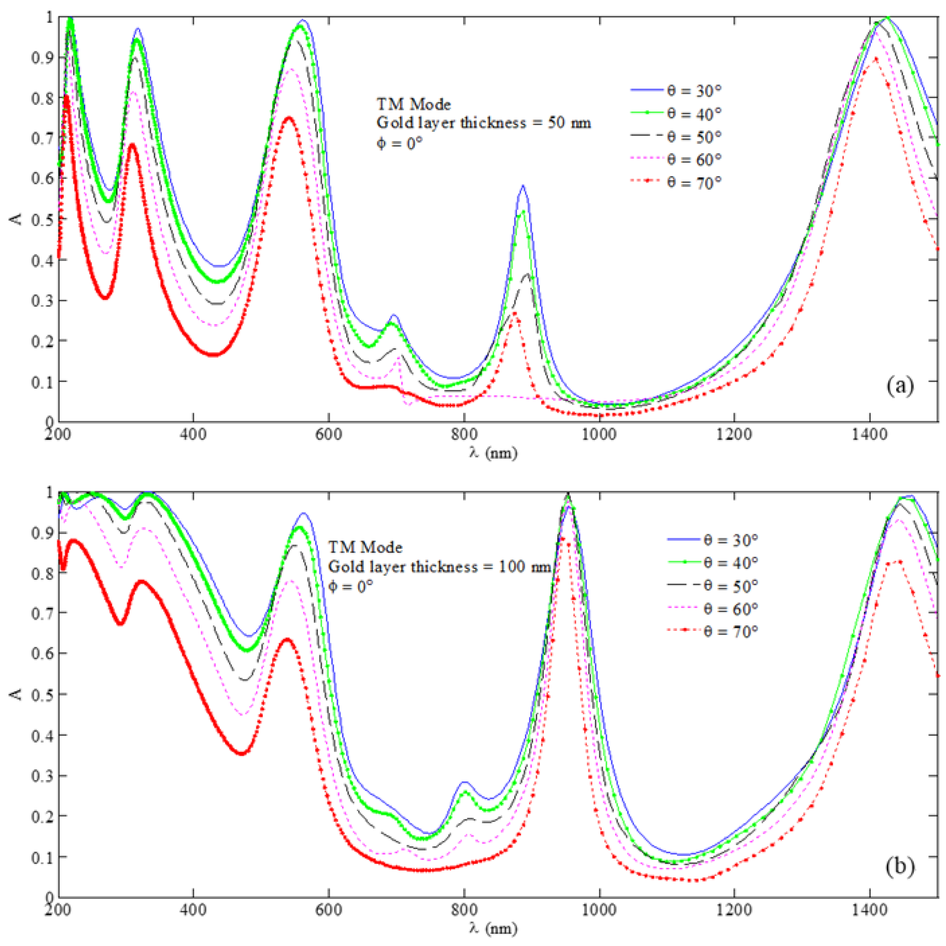
Absorption patterns corresponding to the TM-polarized incident waves (
Figure 6) are almost similar to that obtained for the TE excitation (
Figure 3). However, enhanced sharpness and amplification of absorption peaks, as observed for both the values of metasurface thickness (
i.e.,
nm (
Figure 6a) and
nm (
Figure 6b)), are the primary advantages of using the TM-polarized incident field over the TE-polarized one (
Figure 3). It is clear from
Figure 6a that the use of metasurface thickness as 50 nm would yield almost 99.9% absorption at
nm under the situation of
incidence.
Figure 6b shows that the same incidence angle would provide
absorption at
nm when the metasurface assumes 50 nm thickness. It is clear from
Figure 3 and
Figure 6 that such a high amount of absorption is rarely achieved with the TE-polarized incidence excitation except in the long wavelength range (
nm), taking into account 100 nm metasurface thickness (
Figure 3b) and
incidence angle. It can thus be remarked that
Figure 6a,b exhibit a
angle of incidence as promising to achieve the highest absorptivity in this case, which is similar to the situation of
Figure 3 corresponding to the case of TE incidence excitation.
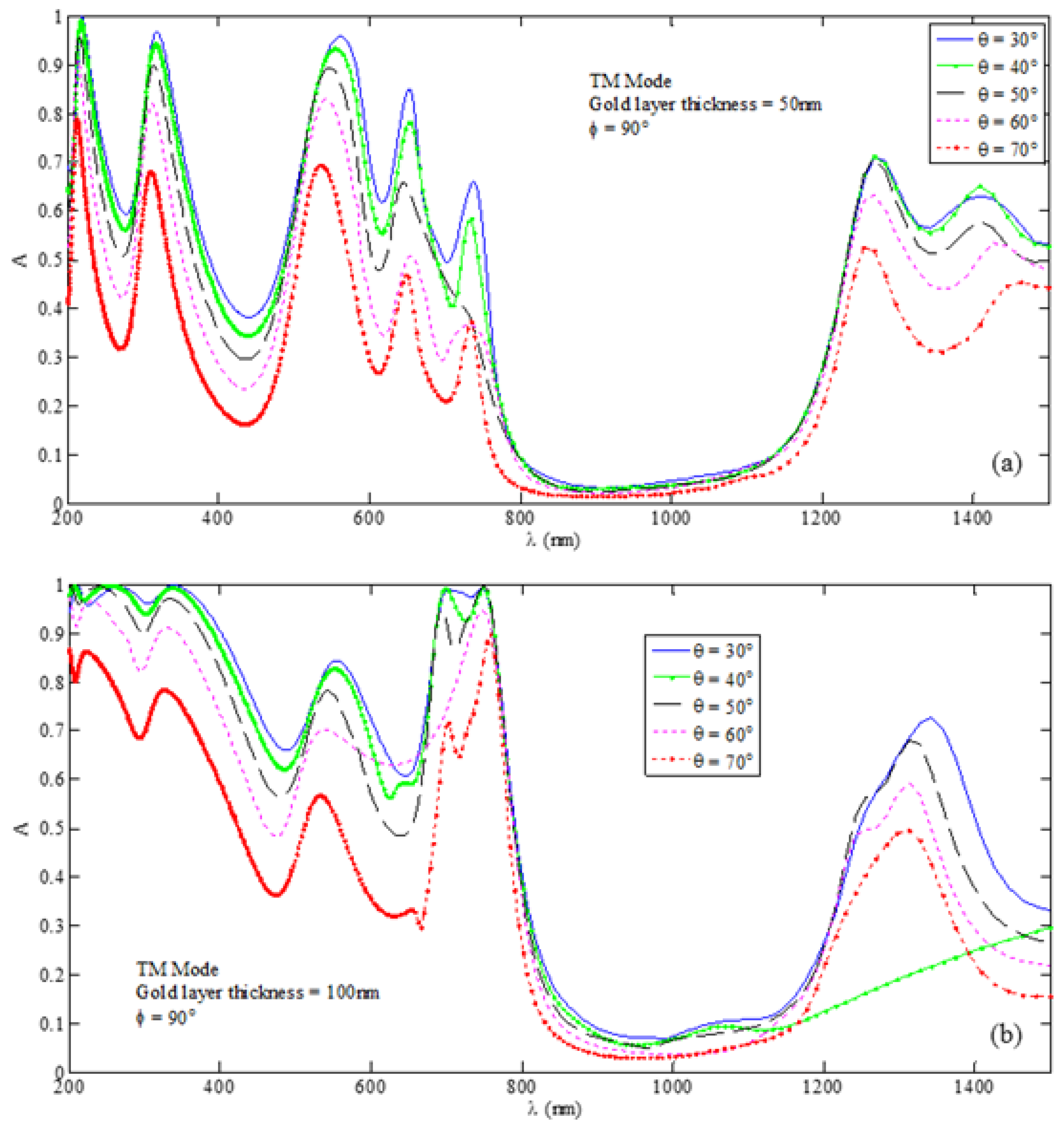
Figure 7 shows absorption spectra of the MPA structure when the Si layer assumes 500 nm thickness. The trend of absorption patterns is observed to be similar to the case of TE-polarized incidence,
i.e., the increase of Si layer thickness enhances the number of sustained modes within the light trapping medium, thereby causing enhancement of absorption peaks. As such, a proper adjustment of the thicknesses of metasurface and wave confinement regions would yield the desired absorption in a particular wavelength span; indeed, the polarization state and the angle of incidence also play very important roles in this regard.
Figure 8 exhibits the plots of absorption under the TM wave excitation with
. The other parametric values are chosen in the same way as those in the case of
Figure 5,
i.e., keeping the Si layer thickness
fixed to 100 nm, the metasurface layer thickness
to 50 nm and 100 nm, and sweeping angle
as
,
,
,
and
. We find that, also in this case, the absorption peaks are not prominent enough (in comparison with those in
Figure 6) for particular usage, and therefore, the choice of
would not be appropriate enough to obtain significantly application oriented results. In the present paper, however, such results are shown just in order to observe the anisotropic features of the metasurface in use.
The absorption characteristics of the MPA structure having different dimensional features are further investigated by incorporating the electric field patterns. However, it must be noted that the presence of multiple peaks in absorption spectra essentially corresponds to different resonant conditions. As such, some of the absorption peaks are chosen that typically exhibit the minimum and the maximum values of absorption under certain dimensional features, incident angles and polarization states of the incidence excitation.
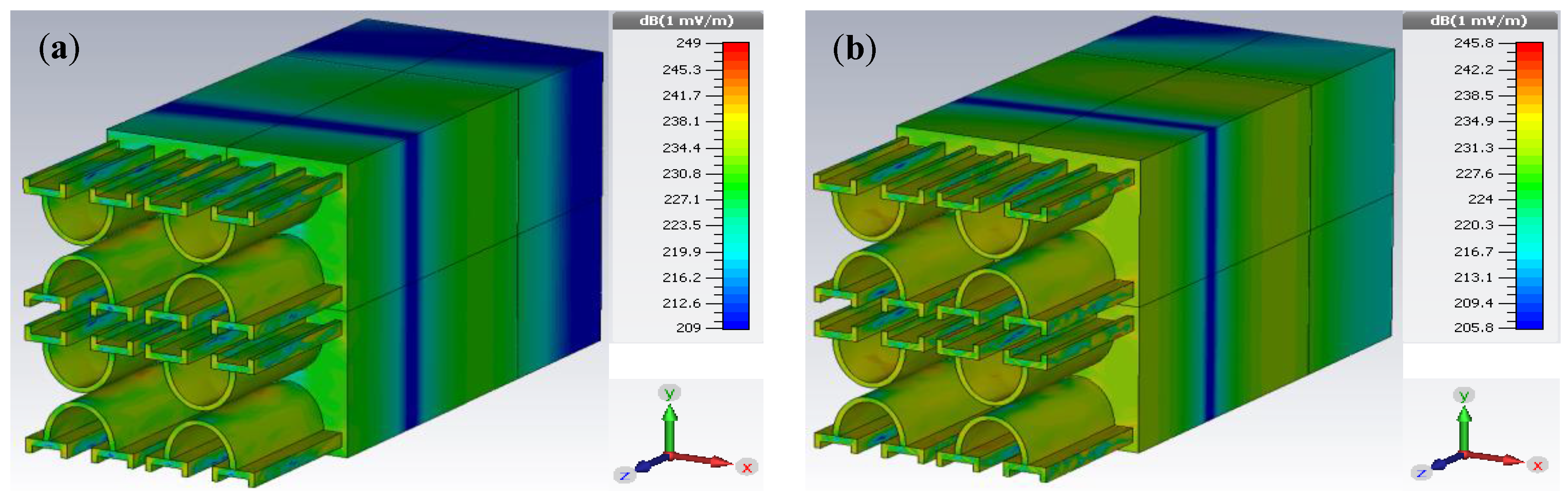
In this context,
Figure 9 and
Figure 10, respectively, illustrate the electric field distribution patterns for the MPA structure with the thickness
(of metasurface) as 50 nm and 100 nm; in both the cases, the thickness
of light trapping medium is taken as 100 nm and the incidence excitation as the TE-polarized one. However, for other dimensional features (of the MPA) and excitation as well, field patterns may be obtained, but those are not incorporated into the text. Instead, typical field distributions for a particular value of the angle of incidence
, as evolved corresponding to the absorption maxima and minima, are considered.
It can be observed from
Figure 3a that, corresponding to the metasurface thickness
as 50 nm, the TE-polarized wave excitation gives the maximum absorbance of 98.8% at
for wavelength
nm, and the minimum absorbance of 74.2% at
for
nm. These situations are, respectively, depicted in
Figure 9a,b, emphasizing the field distributions.
Figure 9a shows that the field is highly concentrated in the Si section (of the MPA structure), and the intensity of field (in this section) is higher than that observed in
Figure 9b (corresponding to the case of lower absorptivity)—the theme which is very much justified from the absorption spectra of
Figure 3a.
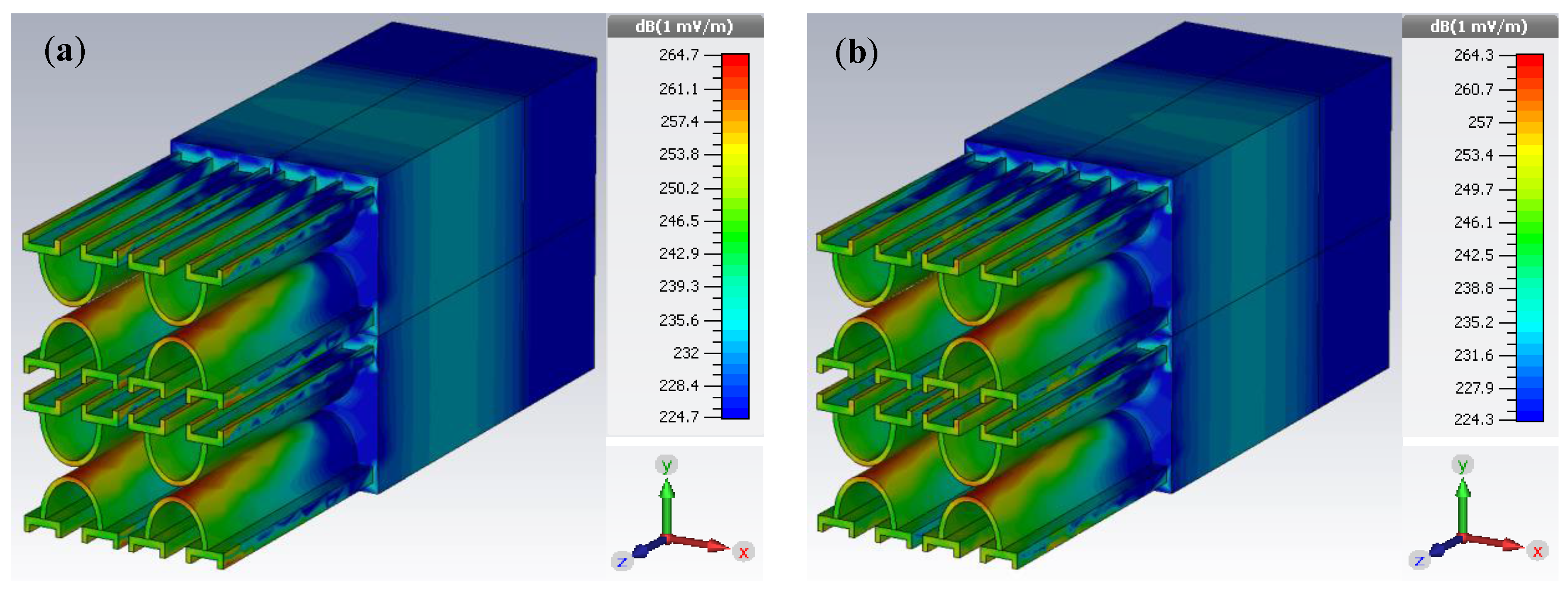
Figure 10a,b respectively, depict the field distributions obtained corresponding to the TE-polarized incidence excitation with the incidence angles
and
, and when the metasurface thickness
is increased to 100 nm. Similar to
Figure 9, also in this case, the field configurations are obtained for the wavelength values that yield the maximum (for
nm,
) and the minimum (for
nm,
) absorption. It can be noticed that the increase of metasurface thickness causes the electric field to extend to the lower edges of nanostructured resonator, except for its confinement in the Si layer. In the case of larger thickness of metasurface, the electric field exhibits significant coupling with the edges of the metamaterial structure. The absorption of incident waves happens due to the confinement of electric field on the edges of metallic resonator. With the increase in incidence angle, the field starts entering the substrate region, thereby reducing the absorbance.
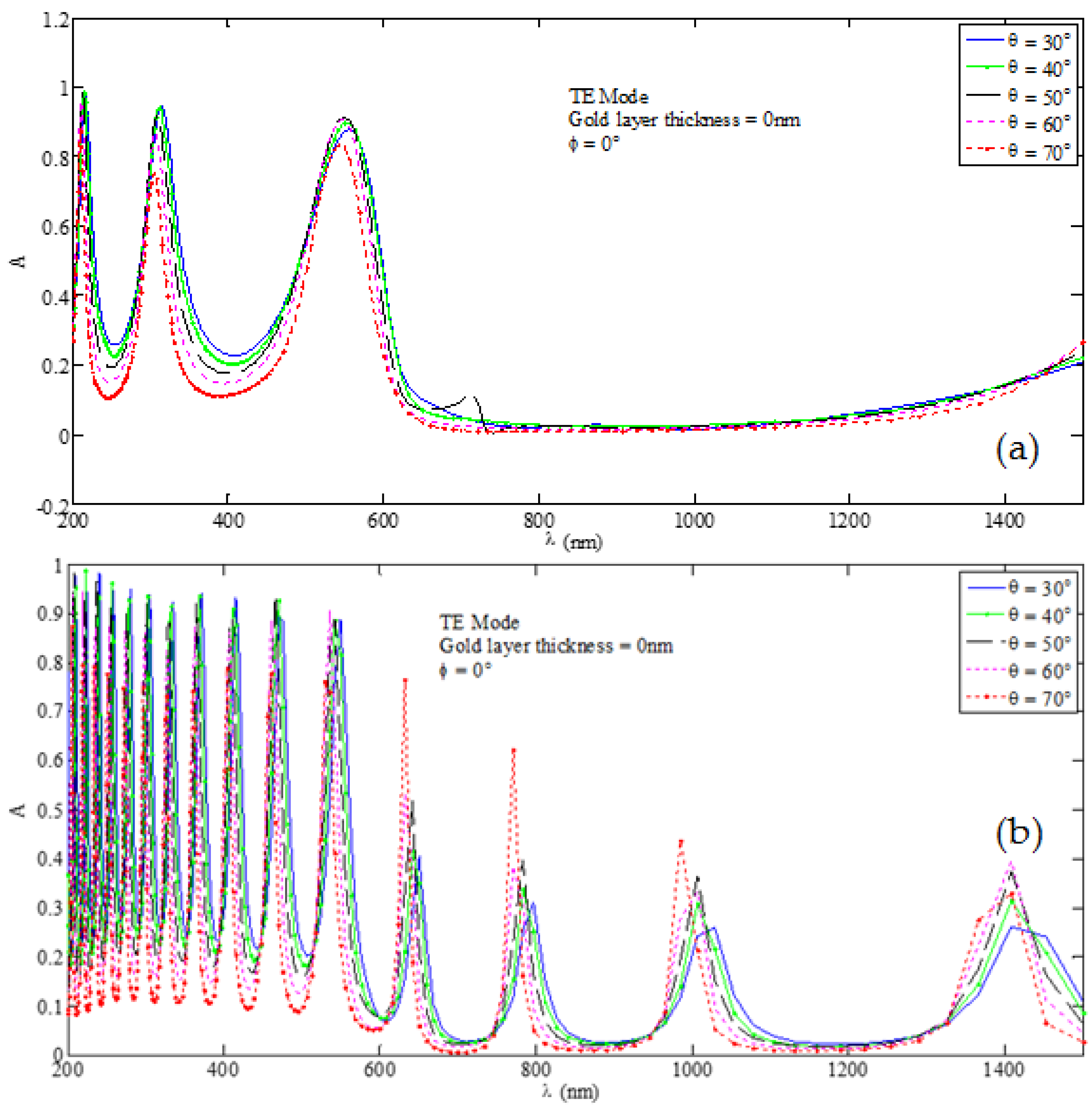
Along with the afore-discussed issues of the absorption characteristics of the device, one may think of the features of absorbance that may be achieved in the absence of nanoengineered gold metasurface (shown in
Figure 1). With this view point, the results are obtained corresponding to the excitations of TE (
Figure 11) and TM (
Figure 12) modes with the sweep in
as
,
,
,
and
. As the upper layer is now isotropic in nature, the angle
will essentially have no effect on the results. Further, similar to the previously discussed cases, we consider two values of the Si layer thickness, viz.
nm and
nm.
Figure 11a,b, respectively, illustrate the absorption characteristics corresponding to the Si layer thickness as 100 nm and 500 nm, and in the absence of metasurface layer (
i.e.,
). Comparing the results in
Figure 3 and
Figure 11a, we observe that, under the TE mode excitation, the presence of metasurface enhances the number of absorption peaks particularly in the longer wavelength range. Clearly, the peaks in regions with
nm and
nm vanish in the absence of gold metasurface. Also, the variation in
has more profound impact on the absorbance in the presence of metasurface, which is essentially due to the plasmonic effect. Further, the increase of the Si layer thickness to 500 nm certainly enhances the number of peaks (
Figure 11b), but the comparison of these results with that in
Figure 4 clearly indicates the enhancement of absorption in the mid to the longer wavelength ranges of operation. As such, the efficacy of the presence of gold metasurface is justified as the device can then exhibit significantly improved features of absorption.
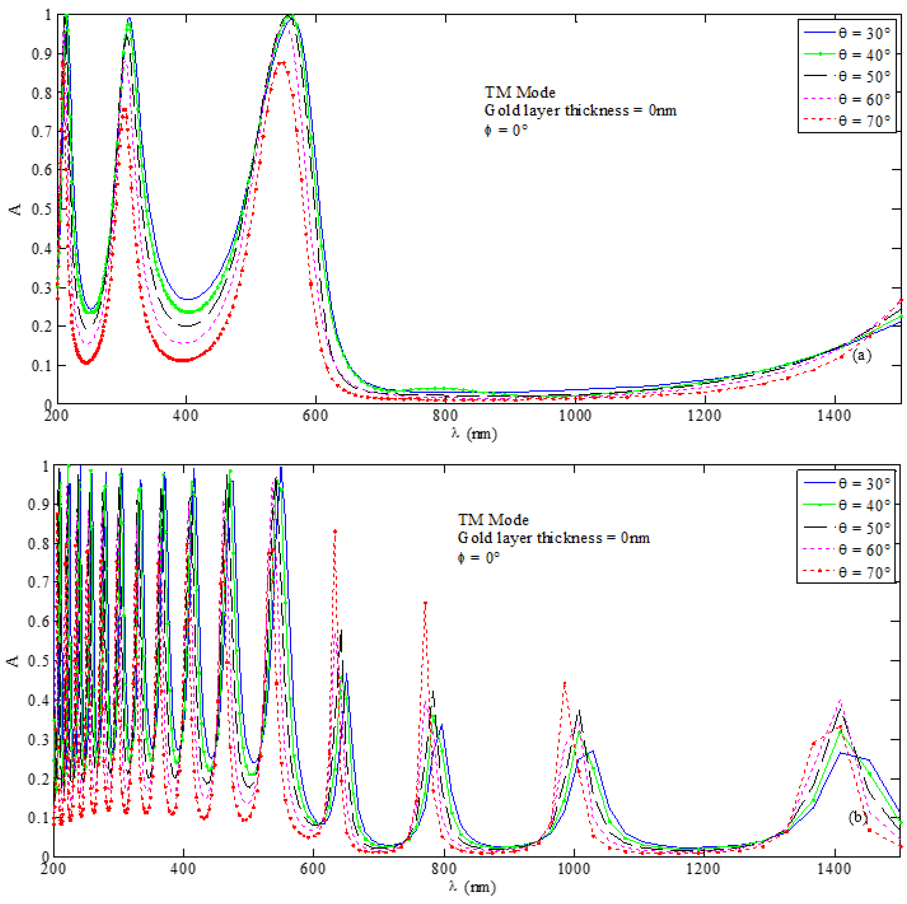
Similar characteristics can be observed corresponding to the TM mode excitation as well, upon comparing the results of
Figure 12 with those in
Figure 6 (for
nm) and 7 (for
nm). We notice that the elimination of gold metasurface greatly affects the absorption patterns in the form of reducing/eliminating absorbance in the longer wavelength range, irrespective of the chosen values of the Si layer thickness. Angular variations also result in a similar way to that described above.
Finally, the novelty of the proposed MPA design lies in that the device would yield nearly 100% absorption of the incidence waves in the visible region of the EM spectrum—the feature that would find potential applications in miniaturized EM energy harvesting gadgets. Apart from this, the device would also be useful in filtering applications in a wide range of wavelengths, as evidenced by the absorption spectra.

