Abstract
This paper introduces a new two-stage multi-parallel-channel LED driver using a CLL-C resonant converter as the first stage and a Time Division Multiple Control circuit as the second stage. The first stage of the proposed converter topology has been developed from CLL-C topology with an additional inductor in the primary side and a capacitor in the secondary side. The converter provides a constant current at a resonant frequency with a Zero Phase Angle (ZPA), thus achieving Zero Voltage Switching (ZVS) turn-on, nearly Zero Current Switching (ZCS) turn-off for the switches, and ZCS for the diodes. The Time Division Multiple Control (TDMC) circuit was applied in the second stage to share the balanced current to each LED string. A 200 W prototype with five output channels was implemented to verify the superior advantages of the proposed topology with a maximum efficiency of 95.05%.
1. Introduction
Recently, high-brightness LEDs have been widely used in general-purpose lighting, back-lighting of LCDs, streetlights, healthcare, and automotive applications because of their superior performance compared to conventional fluorescent lamps, such as their high light efficiency, long lifespan, compact size, and very low maintenance cost [1,2,3].
LEDs typically require a constant current, which can be supplied by an electronic circuit commonly known as a driver [4,5]. The easiest structure to balance the current in LED strings is a series structure [6]. However, this requires a high voltage bus and has poor reliability. If one LED light fails, the whole light system will not work. Therefore, parallel LED strings are a common structure in practice. But current balancing is a significant challenge because of the LED’s exponential voltage–current characteristic and the different temperature coefficient of its voltage drops. Additionally, both the number of LEDs in each string and the number of strings can differ depending on the application. Therefore, a current balancing technique is essential for multiple-string LED applications [7,8].
In conventional techniques, the LED driver typically includes a front-end converter and a multichannel constant-current circuit as the second stage. The passive current balancing method using passive components like capacitors, coupled inductors or balancing transformers, and diodes is an approach that balances the output current [7,9,10,11,12,13,14,15,16,17,18,19,20,21,22,23,24]. Specifically, capacitors are used for passive current balancing in [9,10,11,12,19,22,23], while magnetic components such as transformers and coupled inductors are employed in [13,14,18]. Meanwhile, LCL filters and diodes are utilized for current balancing in [7,15,16,17,20,21,24]. However, these kinds of techniques require a large number of components, which increases the volume and cost, and also results in low efficiency.
Active current balance methods are used to maintain the constant current in each channel by controlling the switches in each channel individually [25,26,27,28,29,30,31,32,33,34]. Therefore, the current of each string can be controlled precisely and there are no imbalance issues. However, this active method requires many components such as switches and control ICs. Moreover, since the current of each LED string is controlled individually, it makes the system complex to control and needs many feedback circuits. Furthermore, the power loss of switches caused by hard switching is one of the main problems leading to low efficiency [35].
The Time Division Multiple Control (TDMC) technique has been introduced and used in the second stage to balance the output current of multiple LED strings [28,29]. Reference [28] presented a compact single-inductor multiple-output parallel string LED driver with a time-multiplexing control. This approach allows for the independent optimization of the local bus voltage, which helps reduce power loss. Moreover, a single time-shared control loop regulates the current in multiple parallel strings, simplifying the control design. However, this method requires numerous control switches and associated feedback circuits, resulting in increased costs and system complexity. In [31], a single-inductor current regulation topology was proposed using a time-division multiplexing control scheme developed from [18]. The topology balances the average current in each channel by connecting the current-delivering inductor to each LED channel for the same period. Despite these improvements, the design suffers from hard-switching operations, which significantly reduce efficiency, typically achieving below 91%.
Similarly, ref. [30] presented an active current balancing approach where individual switches and feedback circuits are used for each LED channel. While this method reduces current imbalance issues, it comes at the cost of increased control complexity. Furthermore, the hard-switching nature of the topology results in substantial switching losses, contributing to its lower efficiency of approximately 88.4%. These limitations make the approach less suitable for high-performance and cost-sensitive applications. In contrast, passive current balancing methods, such as those in [15,17], utilize magnetic components like inductors and transformers to maintain current balance. However, this increases the system’s size and cost, while also compromising reliability.
To address these challenges, the proposed two-stage LED driver combines a CLL-C resonant converter with a TDMC circuit, which has significant advantages. The resonant converter ensures soft-switching conditions (ZVS turn-on and ZCS turn-off), minimizing switching losses and enabling higher efficiency. The TDMC circuit eliminates the need for feedback circuits by balancing the current through the equal time-sharing of each LED channel, simplifying the control strategy. This design not only achieves a peak efficiency of 95.05%, but it also reduces the number of components, making it cost-effective and compact. These features position the proposed topology as a superior alternative for multi-parallel-channel LED driver applications.
This paper is divided into six sections. In Section 2, the First Harmonic Approximation (FHA) will be used to analyze the characteristics of the proposed converter, and the operation principle will be explained in detail. In Section 3, a detailed design methodology for the proposed converter is presented. Section 4 shows the experimental results of a 200 W two-stage LED driver prototype. The comparison of the proposed topology with other topologies is given in Section 5. Finally, the conclusion is given in Section 6.
2. Operating Principle
2.1. The Structure of the Proposed Converter
The structure of the proposed LED driver is shown in Figure 1. It consists of a resonant CLL-C converter as the first stage and the time-division controlled switches (–) as the second stage. In the first stage, the CLL-C converter, operating at resonant frequency, provides a constant current while achieving ZPA for the input impedance, ensuring that all the switches and diodes have ZVS and ZCS. In the second stage, the switches to are controlled by a time-division technique to adjust the running time of each LED string. As a result, the total output current is shared equally among each LED string.
Figure 1.
Configuration of the proposed LED driver system.
From a control perspective, the first stage of the proposed converter operates at a fixed switching frequency with a constant total output current. In the second stage, the frequency and duty cycle of the secondary-side switches (–) are fixed over the whole range of loads to share the current among each string evenly. Therefore, the proposed converter is very simple to control.
From the perspective of efficiency, because it always works at the resonant frequency, the converter can achieve ZVS turn-on and nearly ZCS turn-off for all primary switches, allowing the resonant converter CLL-C to achieve high efficiency. In the time multiplex control circuit, all the secondary switches also operate under soft-switching conditions if their maximum frequency is 2m times the frequency of the first-stage converter (where m is the number of parallel LED strings). Therefore, this two-stage LED driver can achieve high efficiency over a wide load range and can be considered a good choice for multiple LED string applications
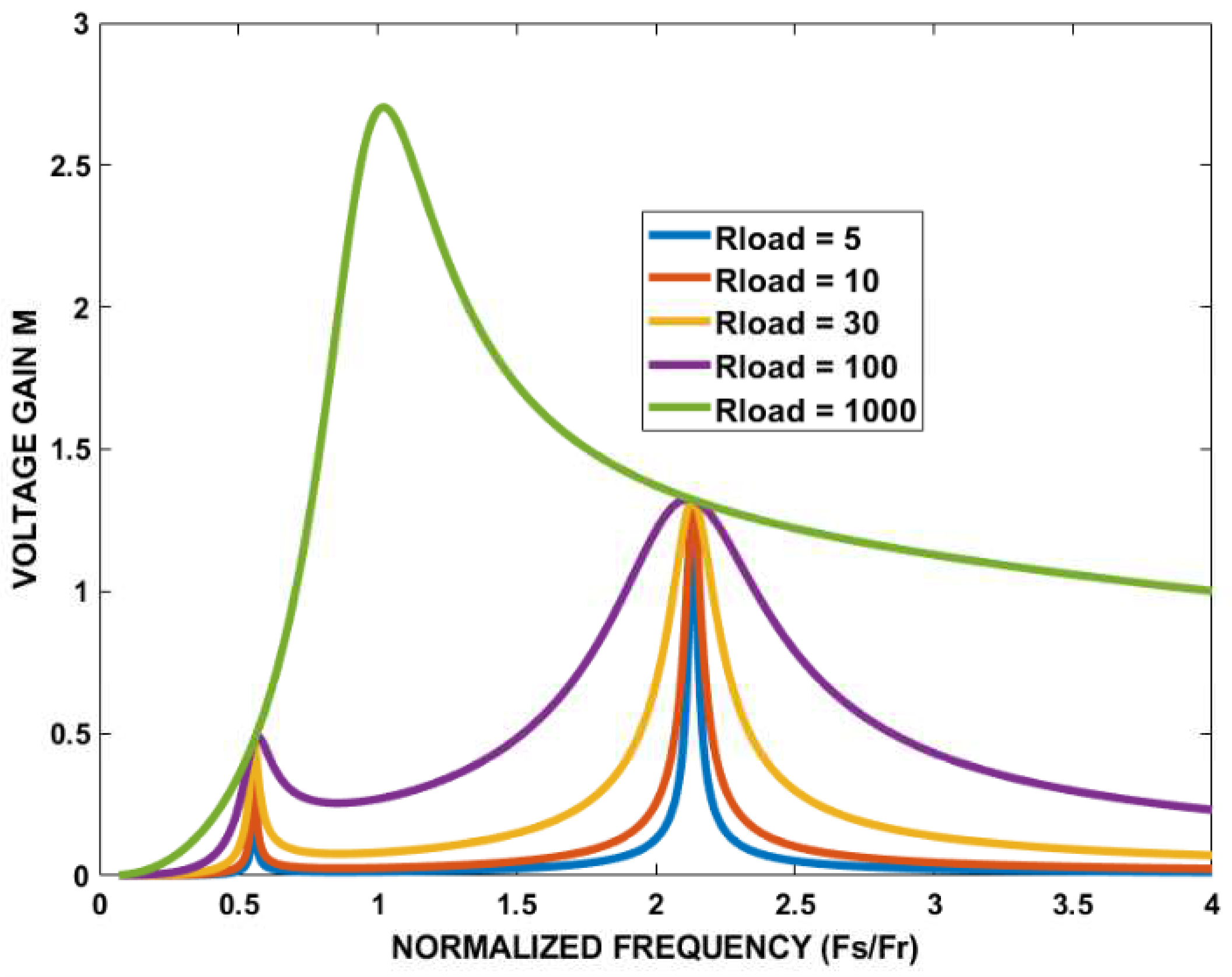
2.2. First Harmonic Approximation Analysis
In order to understand the working principle and the features of the proposed converter, a First Harmonic Approximation (FHA) was applied, and an equivalent circuit is shown in Figure 2.
Figure 2.
FHA equivalent circuit of the proposed bidirectional converter system.
The input voltage of the resonant network is a rectangular output waveform of the half-bridge inverter. The fundamental harmonic approximation of the input voltage can be expressed as in (1):
where is the DC input voltage of the converter system, is the time parameter, and is the switching frequency.
The constant current resonant frequency can be calculated as in (2):
The AC equivalent output resistance can be obtained as follows:
where is the load resistance and is turns ratio of the transformer.
The transfer function of the resonant tank can be derived as in (4):
where , , are the primary-side impedance, magnetic impedance, and secondary-side impedance, respectively. And they are defined as follows:
Then, the voltage gain of the proposed converter versus the operating switching frequency can be calculated as in (8):
The transconductance gain of the converter can be derived as follows:
At constant current resonant frequency , the transconductance gain of the proposed converter can be calculated as shown in (10):
From (10), we can see that the output current is only dependent on the input voltage, the value of the magnetizing inductance, and the constant current resonant frequency.
The input impedance of the proposed converter can be expressed as follows:
At a constant current resonant frequency , the input impedance can be derived by using (2), (5), (6), (7) and (11).
Figure 3 shows the voltage gain M versus the operating frequency under different load conditions from 5 ohm to 1000 ohm, Figure 4 shows the transconductance gain curves with different load condition, and the phase angle of the input impedance versus the operating frequency under different load conditions is shown in Figure 5. From these figures, it can be seen that the proposed converter provides a constant current with ZPA at the constant current resonant frequency in which the capacitor resonates with the inductors and . So, the switches will have ZVS turn-on and nearly ZCS turn-off, as well as ZCS turn-off for diodes.
Figure 3.
Voltage gain M versus the Normalized Frequency () under different load conditions.
Figure 4.
Transconductance gain G versus the operating frequency under different load conditions.
Figure 5.
Phase angle of the input impedance versus the operating frequency under different load conditions.
2.3. Working Principle of Proposed Converter
The working principle of the proposed converter can be divided into eight modes. Figure 6 shows key waveforms of currents and voltages of switches and diodes, and Figure 7 shows the equivalent circuits of the proposed converter in different modes of operations. The following assumptions are made to simplify the analysis: All the components are ideal. The transformer has a turns ration of n:1 where n is the primary-side turn number. The leakage inductor is placed in the secondary side.
Figure 6.
Key waveforms of the proposed converter.
Figure 7.
Equivalent circuits of the proposed converter in different modes.
Mode 1: []
This is the dead-time period between the switches. At , is turned off with nearly ZCS, and is nearing zero. The parasitic capacitor of is charging and raising the voltage across , where the parasitic capacitor of is discharging and creating the ZVS turn-on condition for . The resonant tank and the magnetizing inductor are discharging and transferring power to the secondary side. In the secondary side, the diodes and are forward biased, the diodes and are reverse biased.
Mode 2: []
At , turns on with ZVS and the primary current zero, and the body diode of is forward biased for a very small amount of time. The resonant tank and the magnetic inductor are still discharging as in Mode 1 and transferring power to the secondary. At the end of this mode, the resonant tank is nearly fully discharged.
Mode 3: []
At , is on, and in the start of this mode, the resonant tank starts to charge. The primary current flows through , while the magnetizing inductance is discharging in the start and starts charging in the middle of this mode. Power is transforming in the same direction as in Mode 1 and 2 till the end of this mode. The capacitor resonates with inductor and .
The primary current in this mode can be calculated as in (13):
The primary current at is shown in (14):
And the impedance of the resonant tank can be derived as follows:
where is the voltage across and is the switching period.
In addition, the magnetizing current can be expressed as in (16):
At the end of this mode, the primary current equals to the magnetizing current . The resonance between the capacitor and inductors and is halted, and the power is not transferred to the secondary side anymore. In the secondary side, the current through the diodes current and becomes zero, creating the ZCS turn-off condition for these diodes. At the end of this mode, the diodes and are turned off with ZCS, and the diodes and are turned on.
Mode 4: []
At , in this mode, the capacitor resonates with inductors and , and the power starts transforming to the secondary side. The rectifier diodes and are reverse biased, and the diodes and are forward biased.
The primary current in this mode can be derived as follows:
The impedance of the resonant tank in this mode is shown in (18):
Mode 5: []
This mode is the second dead-time period for the switches. At , turns off with nearly ZCS, and the parasitic capacitance capacitor of is charging and raising the voltage across , where the parasitic capacitor of is discharging and creating the ZVS turn-on condition for . The operation during this mode is similar to Mode 1. However, the charging and discharging of the parasitic capacitors of the switches is changed on the contrary in comparison to Mode 1.
Mode 6: []
At , is off. turns on with the ZVS that was created in Mode 5 and its body diode is forward biased. The capacitor starts to resonate with inductors and . In the secondary side, diodes and are reverse biased, and the diodes and are forward biased, as in Mode 5. At the end of this mode, the primary current becomes nearly zero and the body diode of is reverse biased.
Mode 7: []
At , the body diode of is reverse biased and the primary current flows through . The resonant path and the operation of the secondary-side diodes are the same as in Mode 6. The primary current has the same magnitude but opposite direction compared to that in Mode 3.
At the end of this mode, the primary current equals to the magnetizing current , and the resonant between capacitor and inductor and is stopped, and the power is not transferred to secondary side anymore. In the secondary side, the secondary-side current becomes zero, the diodes and turn on, and the diodes and turn off with ZCS.
Mode 8: []
At , the capacitor resonates with inductor and , and starts transferring the power to the secondary through the transformer. Diode and are forward biased and diode and are reverse biased. The primary current has the same magnitude but opposite direction compared to that in Mode 4. At the end of this mode, one switching period is complete and is ready for the next cycle.
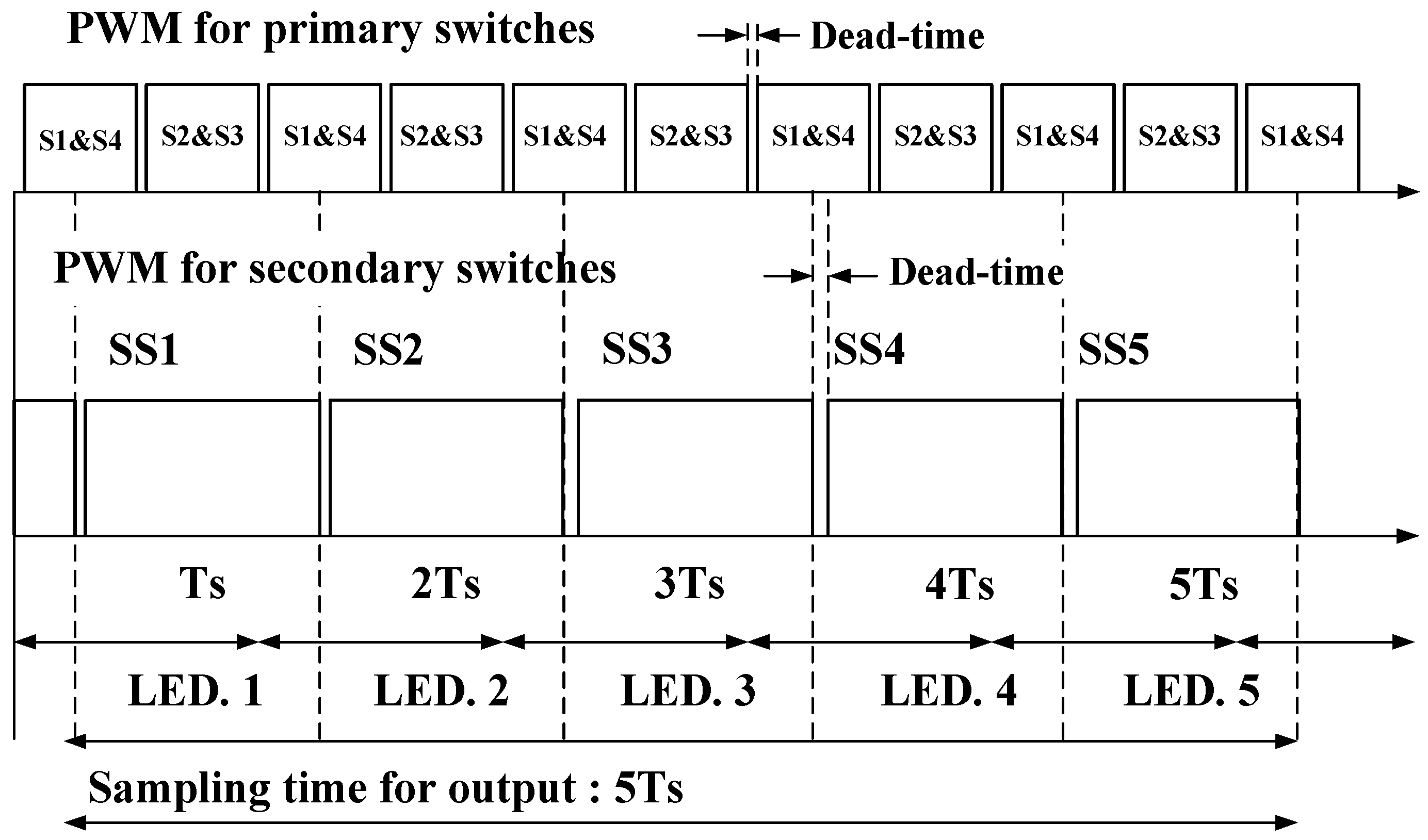
2.4. Operation Principle of the Time Division Multiplex Control (TDMC) Technique
Figure 8 shows the PWM scheme for the second stage of the proposed converter using TDMC for five-channel LED drivers. The working principle of the TDMC method can be explained as follows. The primary-side resonant converter is performed at the constant current resonant frequency of for the primary switches to provide a total constant current Itot for all five LED strings. The secondary stage switches work at the frequency of In order to balance LED output current, all of the outputs are regulated in one sampling time (). In one interrupt cycle, only one secondary switch is turned on to allow the primary side to operate. It means that, one second-stage switch will operate with the duty cycle of nearly 20% and the shifted phase between the switches of two adjacent channels is nearly 72 degrees. As a result, all output currents ( to ) have the same value and the output voltage − of each channel will then settle to the value that makes its average current value equal to , ignoring the current and voltage ripple within the switching period. In the proposed method, the total output is required to regulate constant. Thus, it is possible to provide numerous output channels with highly precise regulations.
Figure 8.
Switching waveforms for the primary and secondary switches of the proposed converter with the Time Division Multiple Control Technique for five channels.
3. Design Consideration
The resonant tank of primary side , , secondary side , , and magnetizing inductance is designed by considering the requirement value of the output current, ZPA condition, and the selection constant resonant frequency .
3.1. The Current Gain, the Magnetizing Inductance and Turns-Ratio of the Transformer
As shown in (10), in order to meet the output current requirement, the current resonant frequency and the value of the magnetizing inductance are designed by the trade-off of the volume of the proposed converter and the losses.
3.2. The Resonant Inductor and Capacitor
After choosing the resonant frequency and the value of the magnetizing inductance, the value of the inductors , , and capacitors , can be chosen based on the resonant frequency and ZCS turn-off condition at the end of Mode 4 and Mode 7 during the operation part. At the end of Mode 4 and Mode 7, the current flows through the switches and is calculated as in (17). From (17), we can see that, in order to achieve nearly ZCS turn-off for the switches, the impedance of the resonant tank as shown in (18), must be as large as possible. Then the value of the inductor and capacitor can be chosen to meet the requirement of (2) and maximum of (17).
The leakage inductance of the transformer is unwanted but also unavoidable. In the secondary side, the leakage inductor resonates with the magnetizing inductor and capacitor at the constant current resonant frequency . Then the value of the capacitor can be calculated as in (18).
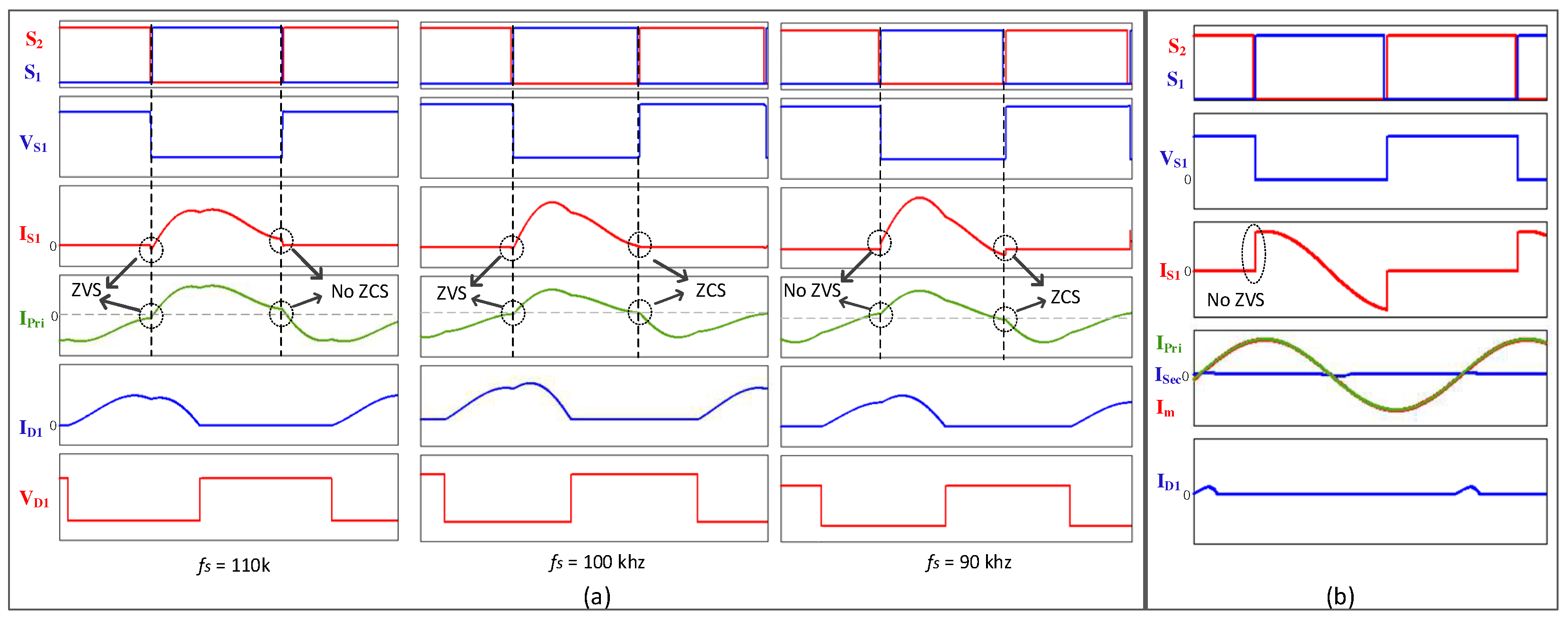
3.3. The Dead-Time of the Switches and ZVS Condition
The dead-time is critical for achieving Zero Voltage Switching (ZVS) by allowing the parasitic capacitance of the switches to charge/discharge fully before switching. As shown in Figure 6, the primary current must remain negative during the dead-time to enable this process. This operation is influenced by the magnetizing current , which depends on the magnetizing inductance . The derived condition for td, given in (20), ensures that ZVS is achieved while minimizing losses. However, excessive td can reduce the effective duty cycle, affecting efficiency.
Experimental waveforms in Figure 9 and Figure 10 confirm reliable ZVS turn-on and nearly ZCS turn-off for the primary switches. The chosen = 330 μH ensures sufficient to fully charge/discharge Coss during the dead-time, as evidenced by the low turn-off current (~0.3 A) in Figure 9. These results validate the design choices, which contribute to the measured peak efficiency of 95.05%.
Figure 9.
Current and voltage waveforms of MOSFET 1 at maximum output power = 200 W.
Figure 10.
Current and voltage waveforms of diode 1 at maximum output power = 200 W.
3.4. Minimum Frequency Analysis and Switching Behavior
The minimum switching frequency plays a crucial role in ensuring soft-switching operation in the proposed resonant converter. It is determined by the condition that the magnetizing current and resonant current must be sufficient to completely discharge the MOSFETs’ output capacitance before turn-on. If the switching frequency is too low, the available energy in the resonant tank becomes insufficient, leading to hard switching and increased switching losses.
The minimum frequency can be estimated using the resonant tank parameters as in (21):
where and are the primary resonant and magnetizing inductances, while and represent the primary resonant capacitor and the MOSFET output capacitance, respectively.
To illustrate this, Figure 11a depicts the soft-switching behavior at different switching frequencies, where ZVS is lost at lower frequencies while ZCS disappears at higher frequencies. Similarly, Figure 11b shows the converter performance under very light load conditions, where ZVS is lost, leading to hard switching.
Figure 11.
ZVS and ZCS (a) at different switching frequencies and (b) during light load.
Maintaining an appropriate switching frequency is therefore critical to achieving efficient operation while ensuring ZVS and ZCS are retained.
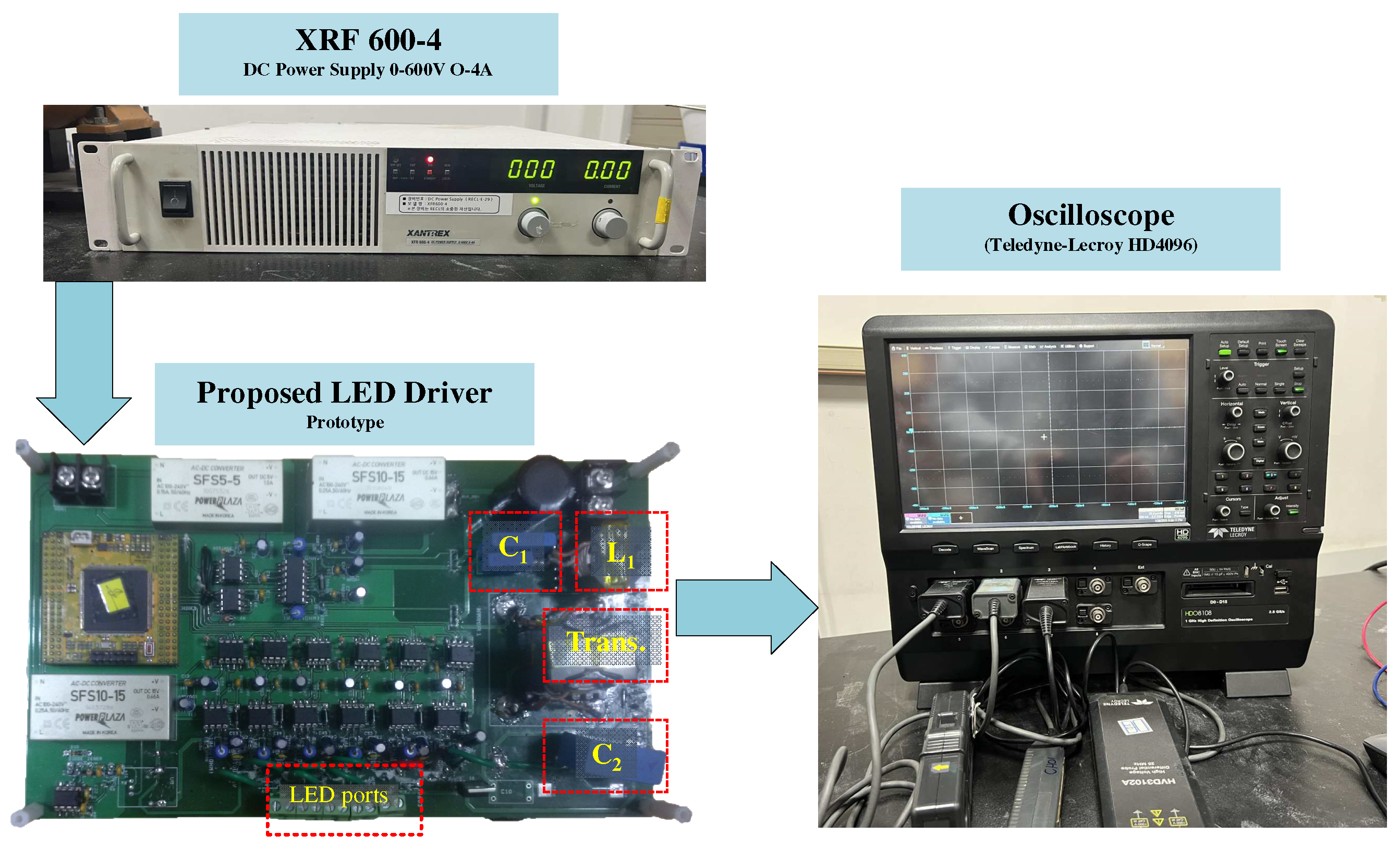
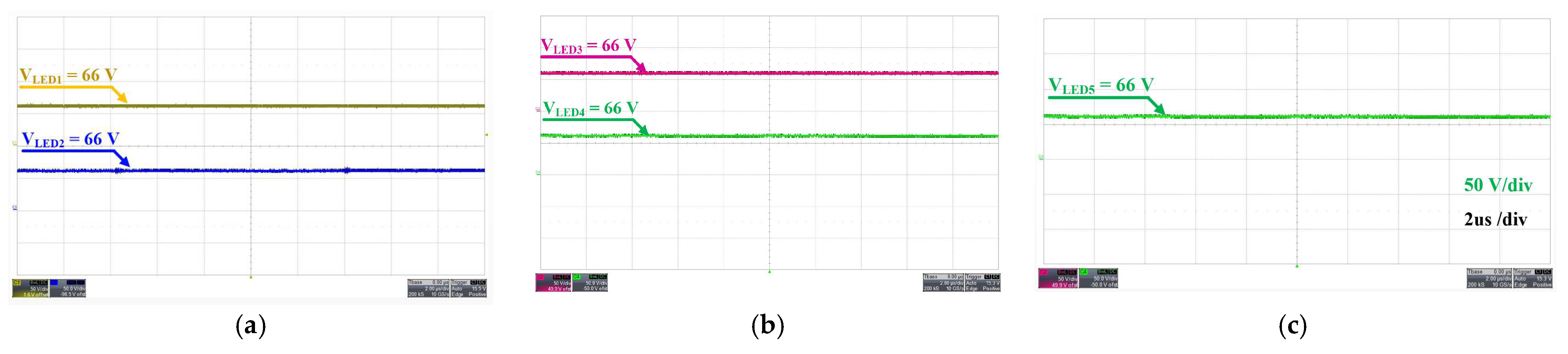
4. Experimental Results
In order to verify the declared features of the proposed converter, a 200 W prototype, with the specifications given in Table 1 and Table 2, was designed, built, and tested. XRF 600-4 DC power supply was used for DC supply, Teledyne-Lecroy HD4096 oscilloscope was used for measurements, and the test was performed at room temperature. An experimental circuit of an LED driver adopting the proposed converter topology experimental setup of the proposed LED driver prototype is shown in Figure 12.
Table 1.
Specification of the proposed converter.
Table 2.
Ratings of the MOSFETs.
Figure 12.
Experimental setup of proposed LED driver prototype.
Figure 11 shows the experimental waveform of primary-side MOSFETs under the maximum output power of 200 W. It is clear that the MOSFETs are turned on with the ZVS condition and turned off with the nearly ZCS condition. The turn-off current is small, just 0.3A. Meanwhile, Figure 12 shows the waveforms of the rectifier diodes in the secondary side. Similarly, ZCS turn-off of the rectifier diodes can be observed from Figure 12, hence there is no circulating current, which reduces the losses of the proposed converter.
Figure 13 and Figure 14 show the measured DC output voltage and current waveforms of each LED channel, respectively. In Figure 13, the voltage of each LED string at the full load condition is 66.6 V. In Figure 14, the current of all LED strings is the same and is equal to 0.57A. This is due to the time division technique. When the driving MOSFET of one LED string is turned on, the driving MOSFETs of the other strings are all turned off. This process is repeated every five switching periods of the primary-side MOSFET. Further, the conduction time of all the LED strings is equal. Moreover, the CLL-C converter stage gives the constant current, so then the average output currents of the LED strings are balanced and kept constant of 570 mA with the variation of the load.
Figure 13.
The voltage waveforms of each LED at maximum output power = 200 W: (a) the first and the second LED strings, (b) the third and the fourth LED strings, and (c) the fifth LED string. (a) Voltage waveforms of the first LED string and the second LED string. (b) Voltage waveforms of the third LED string and the fourth LED string. (c) Voltage waveform of the fifth LED string.
Figure 14.
The output current waveforms of each LED at maximum output power = 200 W: (a) the first LED string and the second LED string, (b) the third LED string and the fourth LED string, and (c) the fifth LED string. (a) The first LED string and the second LED string. (b) The third LED string and the fourth LED string. (c) The fifth LED string.
Figure 15 shows the efficiency of the proposed LED driver in the whole range of load. The maximum efficiency is at 95.05% at the maximum output power of 200 W.
Figure 15.
Efficiency of the proposed LED drivers with various loads.
5. Comparison
In order to demonstrate the advantages of the proposed topology compared to other multi-channel LED driver designs, a detailed comparison is presented in Table 3. The table outlines the component count, soft-switching capability, and peak efficiency of various topologies, including the proposed method. The proposed design achieves a peak efficiency of 95.05%, which is the highest among the compared topologies. For instance, ref. [30] achieves an efficiency of only 88.4% due to its hard-switching operation, which results in significant switching losses. Similarly, ref. [31] achieves 90.8% efficiency but still falls short due to its reliance on hard-switching and the need for complex control strategies involving multiple feedback circuits. By contrast, the proposed topology employs a CLL-C resonant converter that ensures ZVS turn-on for all primary switches and ZCS turn-off for secondary diodes, minimizing switching and conduction losses. This enables a substantial improvement in efficiency over conventional methods.
Table 3.
Comparison of the proposed LED driver with other topologies.
Additionally, the proposed method significantly reduces the component count, especially for magnetic components such as inductors and transformers, which dominate the size, cost, and volume of LED driver systems. For a five-channel system, the proposed design uses only one inductor, one transformer, and two capacitors, whereas [15] requires ten inductors and one transformer, and [17] uses five transformers. This reduction in magnetic components not only lowers costs, but also simplifies the design and improves reliability. Furthermore, the TDMC circuit in the second stage eliminates the need for individual feedback circuits for each channel, as required in [30]. This simplification makes the control strategy more efficient and cost-effective. Compared to designs like [15], which utilize an LCT-T resonant tank for each channel requiring multiple inductors and capacitors, the proposed topology shares components across all channels, offering substantial space and cost savings while maintaining excellent current balancing performance.
The proposed topology achieves a compact and lightweight design by reducing the total number of components, particularly magnetic elements, which are often the largest and most expensive parts in resonant converters. The reduction in magnetic elements contributes to higher reliability and makes the system suitable for applications where space is limited. Furthermore, the soft-switching capability of the proposed converter ensures reduced thermal stress and switching losses, improving overall performance and longevity. The experimental results validate the design choices, demonstrating that the proposed topology achieves the highest efficiency and smallest component count among the compared designs.
In summary, the proposed topology provides superior performance in terms of efficiency, component count, and design simplicity, making it an ideal choice for multi-channel LED driver applications. These benefits are particularly advantageous for cost-sensitive and space-constrained environments, where reliability and efficiency are paramount.
6. Conclusions
This paper proposed a novel two-stage LED driver combining a CLL-C resonant converter and a Time Division Multiple Control (TDMC) circuit to achieve efficient and balanced current distribution across multiple LED strings. The experimental results validated the superior performance of the proposed topology, achieving a peak efficiency of 95.05%—higher than comparable designs—while ensuring ZVS turn-on and nearly ZCS turn-off for primary switches, and ZCS turn-off for secondary diodes. The TDMC approach eliminated the need for individual feedback circuits, simplifying the control strategy and reducing component count, making the system more cost-effective and reliable. Additionally, the compact design minimized magnetic components, lowering overall volume and production costs.
Despite these advantages, there are areas for further improvement. The efficiency under light-load conditions can be further optimized by refining the soft-switching range. Additionally, future work can explore adaptive control techniques to enhance the robustness of current balancing under varying LED configurations. The proposed design provides a strong foundation for high-efficiency, multi-channel LED drivers, making it a promising solution for lighting applications requiring precision and reliability.
Author Contributions
Conceptualization, D.H.T., Z.W. and W.C.; Methodology, D.H.T.; Software, D.H.T. and Z.W.; Validation, Z.W.; Formal analysis, D.H.T. and W.C.; Investigation, W.C.; Resources, W.C.; Writing—original draft, D.H.T. and Z.W.; Writing—review & editing, D.H.T. and Z.W.; Visualization, W.C.; Supervision, W.C.; Project administration, W.C. All authors have read and agreed to the published version of the manuscript.
Funding
This research received no external funding.
Data Availability Statement
The original contributions presented in the study are included in the article, further inquiries can be directed to the corresponding author.
Conflicts of Interest
The authors declare no conflict of interest.
References
- Bhattarai, T.; Ebong, A.; Raja, M.Y.A. A Review of Light-Emitting Diodes and Ultraviolet Light-Emitting Diodes and Their Applications. Photonics 2024, 11, 491. [Google Scholar] [CrossRef]
- Zissis, G.; Bertoldi, P.; Ribeiro Serrenho, T. Update on the Status of LED-Lighting World Market Since 2018; Publications Office of the European Union: Luxembourg, 2021. [Google Scholar]
- Babris, J.; Avotins, A. Research on Direct Current Power Supply Grid Implementatiopn in Riga Street Lighting System. In Proceedings of the 2022 IEEE 63rd International Scientific Conference on Power and Electrical Engineering of Riga Technical University (RTUCON), Riga, Latvia, 10–12 October 2022; pp. 1–6. [Google Scholar] [CrossRef]
- Gücin, T.N.; Fincan, B.; Biberoğlu, M. A Series Resonant Converter-Based Multichannel LED Driver with Inherent Current Balancing and Dimming Capability. IEEE Trans. Power Electron. 2019, 34, 693–2703. [Google Scholar] [CrossRef]
- Meraj, M.; Rahman, S.; Iqbal, A.; Ben-Brahim, L. High Brightness and High Voltage Dimmable LED Driver for Advanced Lighting System. IEEE Access 2019, 7, 95643–95652. [Google Scholar] [CrossRef]
- Khatua, M.; Kumar, A.; Yousefzadeh, V.; Sepahvand, A.; Doshi, M.; Maksimović, D.; Afridi, K.K. High-Performance Megahertz-Frequency Resonant DC–DC Converter for Automotive LED Driver Applications. IEEE Trans. Power Electron. 2020, 35, 10396–10412. [Google Scholar] [CrossRef]
- Li, Y.; Hu, J.; Li, X.; Chen, F.; Xu, Q.; Mai, R.; He, Z. Analysis, Design, and Experimental Verification of a Mixed High-Order Compensations-Based WPT System with Constant Current Outputs for Driving Multistring LEDs. IEEE Trans. Ind. Electron. 2020, 67, 203–213. [Google Scholar] [CrossRef]
- Teixeira, L.; Loose, F.; Alonso, J.M.; Barriquello, C.H.; Reguera, V.A.; Costa, M.A.D. A Review of Visible Light Communication LED Drivers. IEEE J. Emerg. Sel. Top. Power Electron. 2022, 10, 919–933. [Google Scholar] [CrossRef]
- Wu, X.; Hu, C.; Zhang, J.; Qian, Z. Analysis and design considerations of LLCC resonant multioutput dc/dc LED driver with charge balancing and exchanging of secondary series resonant capacitors. IEEE Trans. Power Electron. 2015, 30, 780–789. [Google Scholar] [CrossRef]
- Baddela, S.M.; Zinger, D.S. Parallel Connected LEDs Operated at High Frequency to Improve Current Sharing. In Proceedings of the 2004 IEEE Industry Applications Conference, 39th IAS Annual Meeting, Seattle, WA, USA, 3–7 October 2004; pp. 1677–1681. [Google Scholar]
- Zhang, J.; Xu, L.; Wu, X.; Qian, Z. A Precise Passive Current Balancing Method for Multioutput LED Drivers. IEEE Trans. Power Electron. 2011, 26, 2149–2159. [Google Scholar] [CrossRef]
- Song, S.; Ni, K.; Chen, G.; Hu, Y.; Yu, D. Multi-Output LED Driver Integrated with 3-Switch Converter and Passive Current Balance for Portable Applications. J. Power Electron. 2019, 19, 58–67. [Google Scholar] [CrossRef]
- Hwu, K.I.; Chou, S.-C. A Simple Current-Balancing Converter for LED Lighting. In Proceedings of the Twenty-Fourth Annual IEEE Applied Power Electronics Conference and Exposition, Washington, DC, USA, 15–19 February 2009; pp. 587–590. [Google Scholar]
- Jung, K.; Yoo, J.; Park, C. Design and Implementation of a Current-balancing Circuit for LED Security Lights. J. Power Electron. 2012, 12, 869–877. [Google Scholar] [CrossRef]
- He, Q.; Luo, Q.; Huang, J.; Cao, C.; Sun, P.; Du, X. LCL-T resonant network-based modular multi-channel constant-current LED driver analysis and design. J. Power Electron. 2020, 20, 1616–1628. [Google Scholar] [CrossRef]
- He, Q.; Luo, Q.; Huang, J.; Cao, C.; Sun, P. Analysis and design of modular open-loop LED driver with multi-channel output currents. IET Power Electron. 2019, 12, 1721–1729. [Google Scholar] [CrossRef]
- Chen, X.; Huang, D.; Li, Q.; Lee, F.C. Multi-Channel LED Driver with CLL Resonant Converter. In Proceedings of the 2014 IEEE Energy Conversion Congress and Exposition (ECCE), Pittsburgh, PA, USA, 14–18 September 2014; pp. 3599–3606. [Google Scholar] [CrossRef]
- Hu, Y.; Jovanović, M.M. A New Current-Balancing Method for Paralleled LED Strings. In Proceedings of the 2011 Twenty-Sixth Annual IEEE Applied Power Electronics Conference and Exposition (APEC), Fort Worth, TX, USA, 6–11 March 2011; pp. 705–712. [Google Scholar] [CrossRef]
- Sedghi, H.; Sarvi, M. A combined capacitor current balancing method with weighting factor control for multi-string LED drivers. IET Circuits Devices Syst. 2023, 17, 135–148. [Google Scholar] [CrossRef]
- Li, D.; Lu, Y.; Ge, X. Fuzzy self-tuning PID control of MC3 LLC resonant LED drivers. J. Power Electron. 2021, 21, 782–791. [Google Scholar] [CrossRef]
- Mukherjee, S.; Yousefzadeh, V.; Sepahvand, A.; Doshi, M.; Maksimović, D. A Two-Stage Automotive LED Driver with Multiple Outputs. IEEE Trans. Power Electron. 2021, 36, 14175–14186. [Google Scholar] [CrossRef]
- Molavi, N.; Farzanehfard, H. Load-Independent Hybrid Resonant Converter for Automotive LED Driver Ap-plications. IEEE Trans. Power Electron. 2022, 37, 8199–8206. [Google Scholar] [CrossRef]
- Chen, S.; Chen, Y.; Zhang, B.; Qiu, D. Very-High-Frequency Resonant Dual-Channel LED Driver With Capacitive Current Balance and Low Voltage Stress on Diodes. IEEE Trans. Power Electron. 2023, 38, 15032–15044. [Google Scholar] [CrossRef]
- He, Q.; Luo, Q.; Wei, Y.; Sun, P. A Variable Inductor Controlled Single-Stage AC/DC Converter for Modular Multi-Channel LED Driver. IEEE Trans. Energy Convers. 2021, 36, 2912–2923. [Google Scholar] [CrossRef]
- Hwang, S.-S.; Hwang, W.-S.; Han, S.-K. Cost-Effective Single Switch Multi-Channel LED Driver. J. Power Electron. 2015, 15, 319–326. [Google Scholar] [CrossRef]
- Chen, H.; Zhang, Y.; Ma, D. A SIMO Parallel-String Driver IC for Dimmable LED Backlighting with Local Bus Voltage Optimization and Single Time-Shared Regulation Loop. IEEE Trans. Power Electron. 2012, 27, 452–462. [Google Scholar] [CrossRef]
- Kim, H.C.; Yoon, C.S.; Jeong, D.K.; Kim, J. A Single-Inductor, Multiple-Channel Current-Balancing LED Driver for Display Backlight Applications. IEEE Trans. Ind. App. 2014, 50, 4077–4081. [Google Scholar] [CrossRef]
- Luo, Q.; Zhu, B.; Lu, W.; Zhou, L. High Step-Down Multiple-Output LED Driver with the Current Auto-Balance Characteristic. J. Power Electron. 2012, 12, 519–527. [Google Scholar] [CrossRef]
- Jha, A.; Singh, B. A Bridgeless Boost PFC Converter Fed LED Driver for High Power Factor and Low THD. In Proceedings of the 2018 IEEMA Engineer Infinite Conference (eTechNxT), New Delhi, India, 13–14 March 2018; pp. 1–6. [Google Scholar] [CrossRef]
- Zu, A.; Luo, Q.; Huang, J.; He, Q.; Sun, P.; Du, X. Analysis and design of a multi-channel constant current LED driver based on DC current bus distributed power system structure. IET Power Electron. 2020, 13, 627–635. [Google Scholar] [CrossRef]
- Yau, Y.-T.; Hwu, K.-I.; Tsai, Y.-D. Development of Four-Channel Buck-Type LED Driver with Automatic Current Sharing. Energies 2021, 14, 7844. [Google Scholar] [CrossRef]
- Jiang, W.Z.; Hwu, K.I.; Shieh, J.J. Four-channel buck-type LED driver with automatic current sharing and soft switching. Appl. Sci. 2022, 12, 5842. [Google Scholar] [CrossRef]
- Xue, L.L.; Ozpineci, B. Adaptive Time-Division Multiplexing Driving System for Solid State Lighting with Multiple Tunable Channels. In Proceedings of the 2021 IEEE Applied Power Electronics Conference and Exposition (APEC), Phoenix, AZ, USA, 14–17 June 2021; pp. 2830–2835. [Google Scholar]
- Zain, M.; Iqbal, S.; Siddique, N. Non-Isolated LED Driver for Industrial Lighting Applications. In Proceedings of the 2023 International Conference on Energy, Power, Environment, Control, and Computing (ICEPECC), Gujrat, Pakistan, 8–9 March 2023; pp. 1–6. [Google Scholar] [CrossRef]
- Esteki, M.; Khajehoddin, S.A.; Safaee, A.; Li, Y. LED Systems Applications and LED Driver Topologies: A Review. IEEE Access 2023, 11, 38324–38358. [Google Scholar] [CrossRef]
Disclaimer/Publisher’s Note: The statements, opinions and data contained in all publications are solely those of the individual author(s) and contributor(s) and not of MDPI and/or the editor(s). MDPI and/or the editor(s) disclaim responsibility for any injury to people or property resulting from any ideas, methods, instructions or products referred to in the content. |
© 2025 by the authors. Licensee MDPI, Basel, Switzerland. This article is an open access article distributed under the terms and conditions of the Creative Commons Attribution (CC BY) license (https://creativecommons.org/licenses/by/4.0/).