Abstract
A non-isolated buck converter, together with resonance and zero voltage transition to achieve zero voltage switching (ZVS) and zero current switching (ZCS), is presented herein to upgrade the conversion efficiency. In this circuit, the main switch and the auxiliary switch are connected to the common ground so as to make the two switches easily driven. Furthermore, these two switches take time division multiplexing operation. In addition, the pulse width modulation (PWM) control technique is utilized so as to render the output inductor and capacitor easily designed. In this paper, the theoretical derivation is first introduced, and secondly, some experimental results are provided to demonstrate the effectiveness of the proposed topology.
1. Introduction
The traditional electronic equipment mostly uses the linear power supply, whose large size and poor efficiency performance have been criticized by the world. Therefore, the switching power supply [1,2] has been developed to improve efficiency as well as to reduce the component size by increasing the switching frequency. Generally, the switching power supply uses hard switching, leading to switching loss and noise. In addition, the switch has to withstand relatively great voltage stress, leading to additional switching loss and conduction loss. Since the switching loss is proportional to the switching frequency, the problem becomes worse. As generally acknowledged, the snubber circuits used in the past are connected in series or in parallel with the switch, which can only reduce the noise when the switch is switched and cannot effectively improve the efficiency. Therefore, the soft switching technology was born to improve the efficiency [3,4].
As for the load-resonant converter [5], this converter includes an inductor-capacitor resonance tank, which is connected in series or in parallel with the load terminal. Resonance elements participate in the energy conversion process of the converter throughout the entire process. The resonance voltage or current generated by the resonance tank is used to achieve zero voltage or current switching. The current and power of the load can be adjusted by the resonance tank circuit, and the capacity of the load can be adjusted by the ratio of the switching frequency to the resonance frequency. This load-resonant converter is also called a full resonance converter and is mostly used in half-bridge or full-bridge converters, suitable for high-power applications [6].
As to the switch-resonant converter [7], the converter only uses the resonance generated by resonant elements to provide the voltage or current required for zero voltage or current switching when the switch is switched. Resonant elements only partially participate in the energy conversion process of the converter, which is also called a semi-resonant converter or quasi-resonant converter [8,9].
As for the zero voltage/current switching, it can be subdivided into two types, full wave and half wave [10], depending on the circuit topology. Since the resonance is in the full wave type, the zero time is short, and it is not easy to accurately control the switch to switch under zero voltage or zero current. If the switch is cut off at the resonant negative current, an auxiliary circuit must be added to keep the current continuous to avoid voltage surges that may damage the switch. In addition, the reverse current flows through the body diode of the switch, causing the conduction loss to be increased. Although the half-wave type does not have this problem, additional components are required, leading to an increase in cost. Currently, diodes are often added to eliminate negative currents, and the length of time, used for zero-voltage, or zero-current switching is increased. At present, most of these converters have been developed to add auxiliary switches, and their working time is shorter than the turn-on time of the main switch, generally about 1/10~1/5 times of t, the turn-on time of the main switch, which is used to control the resonance process of resonant elements so as to achieve soft switching as well as to realize pulse width modulation (PWM) control [11,12].
As to the zero voltage/current transition, the converter is featured by working under PWM control, and the auxiliary circuit work before or after the main switch is turned on. The auxiliary circuit mainly transfers the voltage or current stress that the switch bears to other places to realize the soft switching of the switch, but it stops working at other times to reduce the loss of the auxiliary circuit. According to its operation behavior, it can be divided into zero voltage transition [13,14] and zero current transition [15,16]. These two methods can transfer energy without resonance to achieve zero voltage/current switching of the switch, so that the switching components are free from the high voltage or current stress due to resonance, but an auxiliary switch must be added to help achieve this goal and the auxiliary switch still has switching loss. Therefore, if the zero voltage or current switching is applied to the auxiliary switch, then additional components must be used, leading to an increase in cost.
In the traditional buck converter, the main switch is floating and does not share the ground with the system, making it need an isolated driver. Furthermore, the resonant circuit plus the auxiliary circuit becomes more and more complicated, and even more switches or diodes are added, thereby increasing the cost of components and not effectively improving the efficiency.
In this paper, the proposed auxiliary resonant circuit, with a small number of components, is applied to a traditional buck converter, which is improved by connecting the main switch to the common ground, thereby making the main switch driven relatively easily. Furthermore, the auxiliary switch is also connected to the common ground. In addition, two switches adopt the time division multiplexing operation and the PWM control scheme, thus rendering the circuit components design relatively easily. Above all, both the main switch and the auxiliary switch have ZVS turn-on and ZCS turn-off.
2. Basic Operating Principle
Figure 1 shows the proposed circuit, including the main power stage and the auxiliary stage, and these two stages are controlled by time division multiplexing. The main power stage is constructed by a buck converter with a main switch S1 having a common ground, an output diode D1, an output capacitor C, and an output resistor R. The auxiliary power stage is built up by an auxiliary switch S2, an auxiliary diode D2, a resonant inductor Lr, and a resonant capacitor Cr. The auxiliary diode D2 makes the current flow through the auxiliary switch S2 in a half-wave form. There are six operating states, and Figure 2 shows the relevant waveforms for the circuit operating.
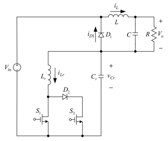
Figure 1.
Proposed resonant buck converter.
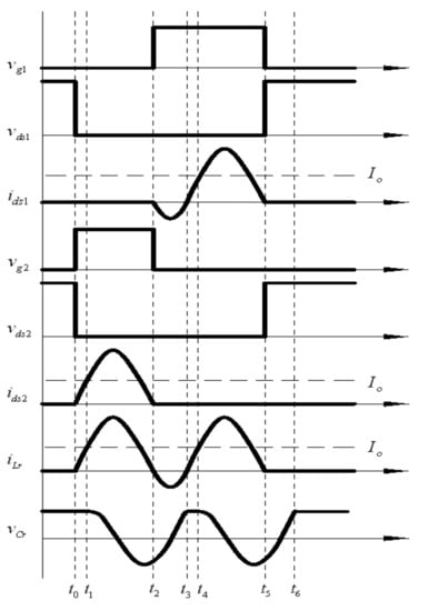
Figure 2.
Illustrated waveforms relevant to the proposed resonant buck converter operating.
State 0 (): As shown in Figure 1and Figure 2, before the switch S2 is turned on, the current Io flows through the diode D1. During this state, the voltage across Cr is the input voltage Vin. Once the switch S2 is turned on, the operation goes to state 1. The corresponding equations are shown as follows:
State 1 (): As shown in Figure 1, Figure 2and Figure 3, the main switch S1 is off but the auxiliary switch S2 is on, whereas the output diode D1 and the auxiliary diode D2 both are on. After the voltage drop across S2 reaches zero, the current flowing through S2 gradually rises and, hence, S2 has ZVS turn-on. Since the resonant voltage vCr is clamped at the input voltage Vin and the output diode D1 is still not cut off, making the resonant capacitor Cr open-circuited, the inductor current iLr rises linearly. As soon as iLr rises to Io, D1 is cut off and the operation proceeds to state 2.
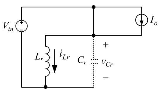
Figure 3.
Equivalent circuit in state 1.
The corresponding initial condition is
The corresponding equation based on Figure 3 and Equation (1) can be described as
At the time instant of t1, the result is
Therefore, based on Equations (3) and (4), the corresponding time elapsed is
State 2 (): As shown in Figure 1, Figure 2, and Figure 4, the main switch S1 is off but the auxiliary switch S2 is on, whereas the output diode D1 is off but the auxiliary diode D2 is on. Since S2 continues to conduct, the resonance between the resonant capacitor Cr and the resonant inductor Lr begins to occur. Therefore, Cr begins to send out energy to Lr, making the resonant voltage vCr drop and the resonant current iLr rise.
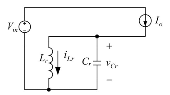
Figure 4.
Equivalent circuit in state 2.
The corresponding initial conditions are
The corresponding equations based on Figure 4 can be described as
By taking the Laplace transform of Equation (7), the resulting equations can be shown in Equation (8):
By solving Equation (8) and then taking the inverse Laplace transform of this solution, the resulting time-domain equations can be obtained as
By substituting the initial values of Equation (6) into (9), the following equations simplified can be obtained as
where
As the resonance starts at the time of t1, iLr continues to rise. When all the energy stored in Cr is sent to Lr, the maximum value of iLr is Io + Vin/Z0. After this peak value, the energy stored in Lr is transferred back to Cr to make VCr rise in the opposite direction and iLr fall. As soon as iLr drops to zero, S2 is turned off, reaching ZCS turn-off. On the other hand, after S2 is turned on in state 1, the voltage across S2 is continuously maintained at zero in state 2, so as soon as the switch S2 is turned off, the switch S1 is turned on immediately, making S1 have ZVS turn-on, and then the operation enters state 3.
At the time instant of t2, the result is
Therefore, based on Equation (10), (11), and (12), the corresponding time elapsed is
State 3 (): As shown in Figure 1, Figure 2, and Figure 5, the main switch S1 is on and the auxiliary switch S2 is off, whereas the output diode D1 and the auxiliary diode D2 both are off. S1 is turned on, taking the role of S2 to continue the resonance, and Lr continues to transfer energy to Cr so that the resonant current iLr goes in the negative direction, and the minimum value of this negative current is Io-Vin/Z0. At the same time, Cr is charged, making vCr continues to rise. Once vCr reaches the input voltage Vin, the operation goes to state 4.
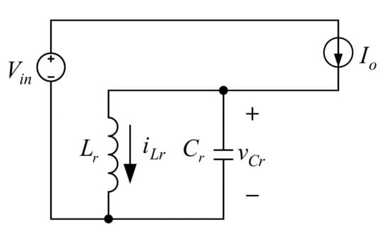
Figure 5.
Equivalent circuit in state 3.
The corresponding initial conditions are
The corresponding equations based on Figure 5 can be described as
By taking the Laplace transform of Equation (15), the resulting equations can be shown in Equation (16):
By solving Equation (16) and then taking the inverse Laplace transform of this solution, the resulting time-domain equations can be obtained as
By substituting the initial values of Equation (14) into (17), the following equations simplified can be obtained as
At the time instant of t3, the result is
Therefore, based on Equations (18) and (19), the corresponding time elapsed is
State 4 (): As shown in Figure 1, Figure 2, and Figure 6, the main switch S1 is on and the auxiliary switch S2 is off, whereas the output diode D1 is on but the auxiliary diode D2 is still off. The resonant voltage vCr is clamped at the input voltage Vin, making the resonant capacitor Cr open-circuited and the resonant current iLr linearly rising. As soon as iLr rises to the output current Io, the operation goes to state 5.
Figure 6.
Equivalent circuit in state 4.
The corresponding initial conditions are
The corresponding equations based on Figure 6 can be described as
By substituting the initial values of Equation (21) into (22), the following simplified equations can be obtained as
At the time instant of t4, the result is
Therefore, based on Equations (23) and (24), the corresponding time elapsed is
State 5: (): As shown in Figure 1, Figure 2, and Figure 7, the main switch S1 is still on and the auxiliary switch S2 is still off, whereas the output diode D1 and the auxiliary diode D2 both are off. The resonant inductor Lr resonates with the resonant capacitor Cr. Cr transfers energy to Lr, so the resonant voltage vCr falls and the resonant current iLr rises. Once S1 is cut off, the operation proceeds to state 6.
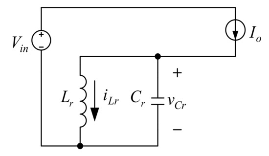
Figure 7.
Equivalent circuit in state 5.
The corresponding initial conditions are
The corresponding equations based on Figure 7 can be described as
By taking the Laplace transform of Equation (27), the resulting equations can be shown in Equation (28):
By solving Equation (28) and then taking the inverse Laplace transform of this solution, the resulting time-domain equations can be obtained as
By substituting the initial values of Equation (26) into (29), the following equations simplified can be obtained as
As the resonance starts at the time of t4, iLr continues to rise. When all the energy stored in Cr is sent to Lr, the maximum value of iLr is Io + Vin/Z0. After this peak value, the energy stored in Lr is transferred back to Cr to make vCr rise in the opposite direction and iLr fall. As soon as iLr drops to zero, S1 is turned off, achieving ZCS turn-off, the operation enters state 6.
At the time instant of t5, the result is
Therefore, based on Equations (30) and (31), the corresponding time elapsed is
State 6 (): As shown in Figure 1, Figure 2, and Figure 8, the main switch S1 and the auxiliary switch S2 are both off. There is no resonance loop. Hence, there is no energy stored in Lr and only the input current Io charges the resonant capacitor Cr, making the resonant voltage vCr linearly rising. Once vCr reaches the input voltage Vin, the output diode D1 is turned on and the operation goes to state 1 with the next cycle repeated.
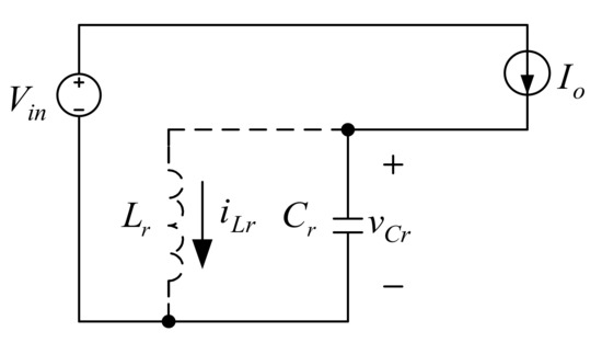
Figure 8.
Equivalent circuit in state 6.
The corresponding initial conditions are
The corresponding equations based on Figure 8 can be described as
By substituting the initial values of Equation (33) into (34), the following simplified equations can be obtained as
At the time instant of t6, the result is
Therefore, based on Equations (35) and (36), the corresponding time elapsed is
3. Design Considerations
Prior to this section, Table 1 shows system specifications. In the following, the design of the resonant inductor Lr and the resonant capacitor Cr is taken into consideration.

Table 1.
System Specifications.
As it is well recognized, the resonant behavior occurs at the resonant radian frequency ω0 and on the condition of ZCS turn-off is , namely, . Therefore, the choice of ω0 and Z0 should be determined first.
Since the voltage conversion ratio is 0.5, then the corresponding duty cycle D is ideally 0.5, meaning that each duty cycle for S1 and S2 is ideally 0.25 due to time division multiplexing operation between the two switches. Accordingly, the resonant frequency f0 is larger than 1 MHz, which is equal to 250 kHz divided by 0.25. Finally, the value of f0 is chosen to be 1.1 MkHz.
After determination of f0, the choice of Z0 follows. From [17], it is assumed that and the value of Z0 locates between and so as to avoid the internal impedance effect. Finally, the value of Z0 is chosen to be , equal to 4.8Ω. In addition, the inequality equations of Lr and Cr are
Therefore, the value of Lr is smaller than 0.69 μH and the value of Cr is larger than 30 nF. Eventually, the value of Lr is 0.65 μH and the value of Cr is 35 nF.
4. Control Strategy
As shown in Figure 9, the resonant buck converter is powered by the input voltage. In the feedback block (VFB), a high-voltage operational amplifier is used to feedback the output voltage. However, because the load and the circuit do not share the same ground, a photocoupler should be used to isolate the two. The feedback signal is sent to the control integrated circuit (IC), named UC3842, to obtain a suitable PWM control signal. Afterwards, this signal is sent to the gate driver to drive the switch so that the output voltage is regulated at the prescribed value.
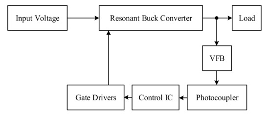
Figure 9.
System configuration block diagram.
5. Experimental Results
The following waveforms are measured at rated load. Figure 10 shows the resonant current iLr and the resonant voltage vCr. Figure 11 shows the gate driving signals vg1 and vg2 for S1 and S2, respectively. Figure 12 shows the gate driving signal vg1 for S1, the voltage across S1, called vds1, and the current flowing through S1, called ids1. Figure 13 shows the zoom-in of Figure 12 for ZVS turn-on of S1. Figure 14 shows the zoom-in of Figure 12 for ZCS turn-off of S1. Figure 15 shows the gate driving signal vg2 for S2, the voltage across S2, called vds2, and the current flowing through S2, called ids2. Figure 16 shows the zoom-in of Figure 15 for ZVS turn-on of S2. Figure 17 shows the zoom-in of Figure 15 for ZCS turn-off of S2. Figure 18 shows the efficiency comparison between with and without the proposed soft switching strategy.
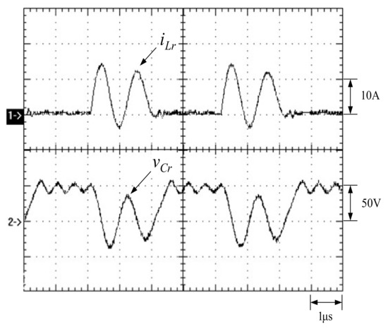
Figure 10.
Resonant waveforms: (1) iLr; (2) vCr.
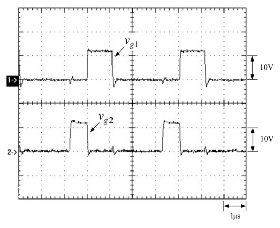
Figure 11.
Gate driving signals for S1 and S2: (1) vg1; (2) vg2.
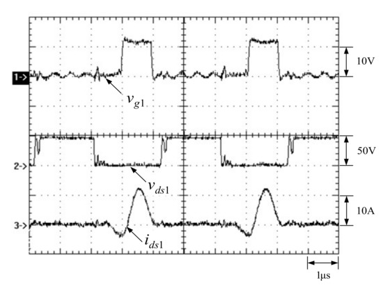
Figure 12.
Waveforms relevant to S1: (1) vg1; (2) vds1; (3) ids1.
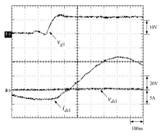
Figure 13.
Zoom-in of Figure 12 for ZVS turn-on of S1.
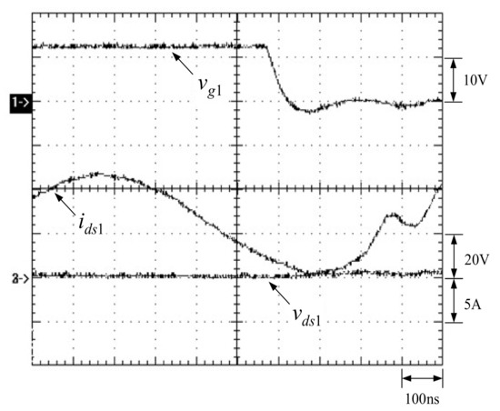
Figure 14.
Zoom-in of Figure 12 for ZCS turn-on of S1.
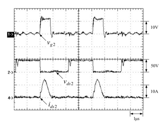
Figure 15.
Waveforms relevant to S2: (1) vg2; (2) vds2; (3) ids2.
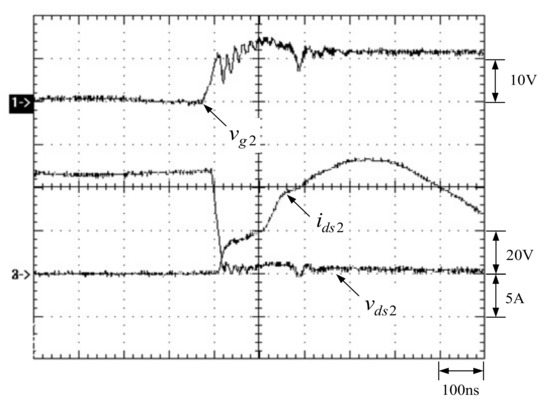
Figure 16.
Zoom-in of Figure 15 for ZVS turn-on of S2.
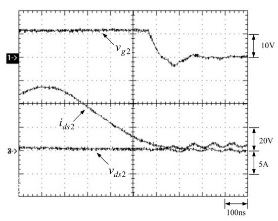
Figure 17.
Zoom-in of Figure 15 for ZCS turn-on of S2.
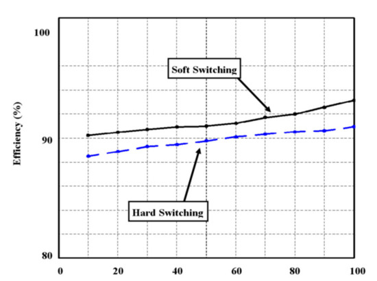
Figure 18.
Efficiency comparison between with (real line) and without (dotted line) the proposed soft switching strategy.
From Figure 10, it can be seen that the peak value of iLr is 14 A, which is smaller than 15 A (=Io + Vin/Io,rated), and the peak value of vCr is 45 V, which is smaller than the input voltage of 48 V. From Figure 11, it can be seen that the switch-on instant for S2 is prior to that for S1 and time division multiplexing operation between S1 and S2 holds. From Figure 13, Figure 14, Figure 16, and Figure 17, it can be seen that the proposed soft switching strategy based on time division multiplexing can make S1 and S2 both have ZVS turn-on and ZCS turn-off. From Figure 18, it can be seen that the maximum efficiencies with and without the proposed soft switching are 92.8% and 90.7%, respectively, and the maximum difference in efficiency between the two is about 2.1%.
6. Comparison
The comparison between the buck-type circuits and the proposed circuit is shown in Table 2, in terms of soft switching features, auxiliary circuit components, output power, output voltage, switching frequency, soft switching strategy, maximum efficiency, and common-ground auxiliary switch. From these comparison items, the proposed circuit has some characteristics: (i) under the smallest number of auxiliary circuit components used, both the main and auxiliary switches have ZVS turn-on and ZCS turn-off; (ii) only the proposed auxiliary circuit has a common-ground auxiliary switch; and (iii) the average performance of the maximum efficiency is mainly due to the highest switching frequency used.
Table 2.
Circuit Comparison.
7. Conclusions
The proposed circuit has several merits described as follows:
- (1)
- The converter adopts an auxiliary circuit with fewer components to realize that both the main and auxiliary switches have ZVS turn-on and ZCS turn-off.
- (2)
- These two switches take the time division multiplexing operation plus the width modulation (PWM) control technique so that the circuit components are designed easily.
- (3)
- The main and auxiliary switches are connected to the common ground so that the two switches are driven easily.
- (4)
- From the experimental results, it can be seen that the maximum efficencies with and without the proposed soft switching are 93.3% and 90.7%, respectively, and the maximum difference in efficiency between the two is about 2.6%.
Author Contributions
Conceptualization, Y.-T.Y. and K.-I.H.; methodology, Y.-T.Y.; software, J.-J.S.; validation, Y.-T.Y., K.-I.H. and J.-J.S.; formal analysis, Y.-T.Y.; investigation, J.-J.S.; resources, Y.-T.Y.; data curation, J.-J.S.; writing—original draft preparation, K.-I.H.; writing—review and editing, K.-I.H.; visualization, J.-J.S.; supervision, K.-I.H.; project administration, K.-I.H.; funding acquisition, J.-J.S. All authors have read and agreed to the published version of the manuscript.
Funding
This research was funded by the Ministry of Science and Technology, Taiwan, under the Grant Number: MOST 110-2221-E-035-050.
Institutional Review Board Statement
Not applicable.
Informed Consent Statement
Not applicable.
Data Availability Statement
No new data were created or analyzed in this study. Data sharing is not applicable to this article.
Conflicts of Interest
The authors declare no conflict of interest.
References
- Erickson, R.W.; Maksimovic, D. Fundamental Power Electronics, 2nd ed.; Electronic Services; Springer Science & Business Media: Berlin/Heidelberg, Germany, 2001. [Google Scholar]
- Weiping, Z.; Zhang, X.; Xiao, S. A Novel Soft Switch for Buck Converter. In Proceedings of the 2nd International Symposium on Power Electronics for Distributed Generation Systems, PEDGS’10, IEEE, Hefei, China, 16–18 June 2010; pp. 180–184. [Google Scholar] [CrossRef]
- Tsai, C.-T.; Shen, C.-L. Interleaved Soft-Switching Coupled-Buck Converter With Active-Clamp Circuits. In Proceedings of the 2009 International Conference on Power Electronics and Drive Systems (PEDS), PEDS’09, Taipei, Taiwan, 2–5 November 2009; pp. 1113–1118. [Google Scholar] [CrossRef]
- Park, K.-B.; Moon, G.-W.; Youn, M.-J. Two-Switch Active-Clamp Forward Converter With One Clamp Diode and Delayed Turnoff Gate Signal. IEEE Trans. Ind. Electron. 2011, 58, 4768–4772. [Google Scholar] [CrossRef]
- Mohan, N.; Undeland, T.M.; Robbins, W.P. Power Electronics: Converters, Applications, and Design, 3rd ed.; John Wiley & Sons, Inc.: Hoboken, NJ, USA, 2002. [Google Scholar]
- Kim, M.; Jeong, H.; Han, B.; Choi, S. New Parallel Loaded Resonant Converter with Wide Output Voltage Range. IEEE Trans. Power Electron. 2018, 33, 3106–3114. [Google Scholar] [CrossRef]
- Chuang, Y.-C.; Ke, Y.-L. A Novel High-Efficiency Battery Charger with a Buck Zero-Voltage-Switching Resonant Converter. IEEE Trans. Energy Convers. 2007, 22, 848–854. [Google Scholar] [CrossRef]
- Jabbari, M.; Najafabadi, N.H.; Shahgholian, G.; Mahdavian, M. A Novel Resonant LLC Soft-Switching Inverting-Buck Converter. In Proceedings of the 2013 10th International Conference on Electrical Engineering/Electronics, Computer, Telecommunications and Information Technology, 3ECTIT’13, IEEE, Krabi, Thailand, 15–17 May 2013; pp. 1–6. [Google Scholar] [CrossRef]
- Qi, J.; Wu, X.; Zhao, Y.; Liu, J. High Step-down ZCS Buck Converter with Switched Capacitor. In Proceedings of the 2020 IEEE Energy Conversion Congress and Exposition (ECCE), ECCE’20, IEEE, Detroit, MI, USA, 11–15 October 2020; pp. 924–929. [Google Scholar] [CrossRef]
- Abu-Qahouq, J.; Batarseh, I. Generalized Analysis of Soft-Switching DC-DC Converters. In Proceedings of the 2000 IEEE International Symposium on Circuits and Systems, IEEE, Geneva, Switzerland, 28–31 May 2000; pp. 185–192. [Google Scholar] [CrossRef]
- Wu, H.; Zhang, J.; Zhao, J.; Zhang, Y.; Hu, L. A New Soft-Switching Synchronous Buck Converter Without Auxiliary Switch. In Proceedings of the 2019 IEEE 10th International Symposium on Power Electronics for Distributed Generation Systems (PEDG), PEDG’19, IEEE, Xi’an, China, 3–6 June 2019; pp. 537–541. [Google Scholar] [CrossRef]
- Ghorbanian, M.; Farzanehfard, H.; Esteki, M. ZVT Flyback With an Active Auxiliary Circuit. In Proceedings of the 2021 12th Power Electronics, Drive Systems, and Technologies Conference (PEDSTC), PEDSTC’21, IEEE, Tabriz, Iran, 2–4 February 2021; pp. 1–5. [Google Scholar] [CrossRef]
- Khorasani, R.R.; Adib, E.; Farzanehfard, H. ZVT Resonant Core Reset Forward Converter With a Simple Auxiliary Circuit. IEEE Trans. Ind. Electron. 2018, 65, 242–250. [Google Scholar] [CrossRef]
- Yau, Y.-T.; Hwu, K.-I.; Jiang, W.-Z. Two-Phase Interleaved Boost Converter With ZVT Turn-On for Main Switches and ZCS Turn-Off for Auxiliary Switches Based on One Resonant Loop. Appl. Sci. 2020, 10, 3881. [Google Scholar] [CrossRef]
- Li, Z.; Zhang, X.; Qian, W.; Bai, H. A Novel Zero-Current-Transition PWM DC-DC Converter With Coupled Inductor. In Proceedings of the 2016 IEEE 7th International Symposium on Power Electronics for Distributed Generation Systems (PEDG), IEEE, Vancouver, BC, Canada, 27–30 June 2016; pp. 1–4. [Google Scholar] [CrossRef]
- Hwu, K.-I.; Shieh, J.-J.; Jiang, W.-Z. Interleaved Boost Converter With ZVT-ZCT for the Main Switches and ZCS for the Auxiliary Switch. Appl. Sci. 2020, 10, 2033. [Google Scholar] [CrossRef] [Green Version]
- Abraham, I.P. Switching Power Supply Design, 2nd ed.; McGraw-Hill: New York, NY, USA, 1998. [Google Scholar]
Publisher’s Note: MDPI stays neutral with regard to jurisdictional claims in published maps and institutional affiliations. |
© 2021 by the authors. Licensee MDPI, Basel, Switzerland. This article is an open access article distributed under the terms and conditions of the Creative Commons Attribution (CC BY) license (https://creativecommons.org/licenses/by/4.0/).