Abstract
This paper proposes a family of high-voltage-gain step-up dc-dc converters for photovoltaic integration application. The proposed converters are capable of converting the low voltage from input sources to a dc bus. The proposed family is constructed of interleaved single-switch multistage boost converters and voltage multiplier cells (VMC). The proposed converters feature low voltage stress across the components, equal current sharing among all phases, and a smooth input current. Moreover, the proposed family of converters has a modular structure in both the VMC and the boost stage. That is, the VMC can have N number of cells, and the boost stage can have k number of stages. The k can be different in each phase, allowing the designers to integrate two independent renewable energy sources with different output voltages. An example converter was explained, analyzed, and simulated. An 80 W hardware prototype was implemented to confirm the converter’s operation and validate the analysis.
1. Introduction
The high-voltage-gain dc-dc step-up converters have become more prevalent in recent years due to the progress in power and energy fields and the development of technologies, such as smart grids, dc microgrids, and dc distribution systems [1,2,3,4,5]. The dc distribution system was found to be an upgrade alternative to the ac distribution system because of the reduced number of conversion units, the capability to protect against grounding faults, superior power quality, and cost-effectiveness. Besides, the dc distribution is desirable for renewable energy sources and battery incorporation to the grid [6,7,8,9,10,11,12]. However, most of the renewable energy sources have low output voltage, which needs to be boosted by about 15–25 times. The most common topology used for stepping up the voltage is the conventional boost converter, which has a simple structure and a low number of components. However, the conventional boost converter’s voltage gain can only be high at extreme duty cycles [13,14,15]. Operating at very high duty cycles increases the voltage stress across the components and requires a large inductance to make the converter draw a continuous input current. With consideration of the conduction and the switching loss, the voltage gain is significantly reduced. Such drawbacks sparked the research for a topology with a high-voltage-gain conversion ratio.
One way to increase the voltage gain is by cascading multiple conventional boost converters, where the output voltage is increased exponentially. Cascading two conventional boost converters allows both stages to operate at a low duty cycle [16,17,18]. Therefore, the voltage stress on the first stage components is low. However, the stress on the second stage output diode still has to block the output voltage. The quadratic converter can be simplified by using only a single MOSFET. The output diode of such a converter suffers from high voltage stress, and the input current has high current ripples [19,20,21]. The voltage stress across components is reduced in the three-level boost converter, and the converter’s size is decreased due to the increase of the effective frequency across the inductor. The three-level boost has the same gain as the boost converter, which is not sufficient for renewable energy applications [22,23]. Switched capacitor circuits are capable of increasing the voltage gain by increasing the number of switching cells. Several advantages can be obtained: high power density, low EMI, the capability of being fabricated into integrated circuit chips. The drawbacks are the inherent losses, a high number of transistors that require isolation circuitry, and gate drivers. Moreover, the output voltage is fixed and cannot be regulated.
Several topologies utilize the transformer or a coupled inductors’ turns ratio to increase the voltage gain as in References [24,25,26,27,28,29]. Using the transformer can meet the requirement of isolation and safety and can provide multiple outputs. However, the power density is significantly reduced, and the weight of the converter is increased. Also, the stress on the MOSFETs caused by the parasitic leakage inductance can damage the switches unless an extra auxiliary circuit is implemented to recycle the energy. Similar to using a transformer, using an integrated coupled inductor improves the voltage gain without providing isolation, such as a hybrid flyback-boost, interleaved with coupled inductors, or quadratic boost converter with coupled inductors. Such topologies suffer from leakage inductance and require extra circuits for circulating the energy and reducing the voltage stress across the switches [30,31,32,33].
This paper introduces an interleaved single-switch multistage boost converter with voltage multiplier cells. The converter features low voltage stress on components and high voltage gain, allows the user to get the most ripple cancellation that interleaving offers, has the capability to integrate different voltage sources, and can match a wide range of loads. Each phase of the interleaved multistage can have either the same or a different number of boost stages than the other phases. This can be very useful for integrating sources with a significant difference in their output voltage. The voltage multiplier cells (VMC) stage uses a bi-fold Dickson that has a symmetrical structure and low voltage stress across the components. Incorporating two symmetrical phases with the same duty cycle yields equal current sharing between the phases and a very smooth input current.
The rest of this paper is structured as follows. First, the theory of operation and steady-state analysis of each mode is presented in Section 2. The components selection and design procedure are presented in Section 3, and the implementation of the hardware prototype and experimental results are explained in Section 4. Finally, conclusions and future work are presented in Section 5.
2. Theory of Operation and Steady-State Analysis
The general structure of the proposed converter is shown in Figure 1. The converter consists of two single-switched multistage boost converter cells. These cells are out of phase, and they are independent of each other, which means each cell can have a different number of the boost stages, as shown in Figure 1b,d. Two independent voltage sources can feed the proposed converter instead of one, which is essential to interface multiple renewable energy sources. The single switch multistage boost converter allows the converter to achieve higher converter gain with no need to add extra MOSFETs and can come in different topologies, as shown in Figure 2. The second stage of the converter consists of voltage multiplier cells to increase the voltage and reduce the voltage stress across the diodes. Numerous VMCs can be used with this converter as in References [34,35,36]. Example converters of the proposed family are shown in Figure 3. In this paper, Bi-fold Dickson VMC is used for the proposed converter, which features lower stress across the diodes and capacitors. Therefore, the voltage gain can be increased in three ways: by increasing the number of VMC cells, by increasing the duty cycle, or by increasing the number of boost stages. The Figure 4 shows the proposed converter with k boost stages and N number of VMC cells. The converter can replace all diodes with MOSFETs to improve efficiency in the case of very high power applications, as shown in Figure 5. The following analysis and experimentation are based on the converter with and , as shown in Figure 6.
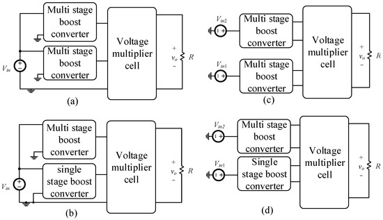
Figure 1.
The general structure of the proposed converter (a) both phases have a multistage boost converter and fed by a single source (b) phases have different numbers of stages and are fed by a single source (c) both phases have the same number of cascaded boost stages, but they are fed by two independent sources (d) each phase has a different number of stages and two independent voltage sources feed them.
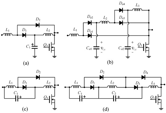
Figure 2.
Multistage boost converters (a) Quadratic cell with a grounded capacitor, (b) Cubic cell with grounded capacitors, (c) Quadratic cell with a floating capacitor, and (d) Cubic cell with floating capacitors.
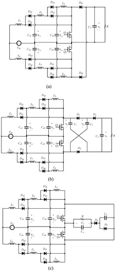
Figure 3.
Different variations of the proposed converter (a) Schematic of the proposed converter with 3 stages (cubic) and no voltage multiplier cell (VMC), (b) another interleaved cubic boost converter with one stage of cross capacitor VMC, and (c) interleaved cubic boost converter with one Cockcroft-Walton cell.
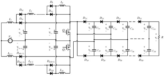
Figure 4.
Schematic of the proposed converter with k boost stages and N voltage mutliplier cells. The voltage gain is .
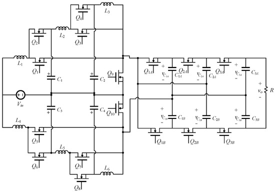
Figure 5.
Schematic of the proposed converter with 3 stages (cubic) and 3 voltage mutliplier cells (tripler) and implemented using MOSFETs instead of diodes to reduce the conduction loss.
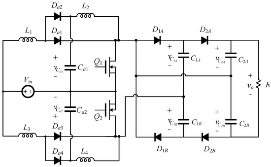
Figure 6.
Schematic of the proposed converter with and .
The analysis of the proposed converter was performed on several assumptions: (1) All components are ideal (2) All capacitors are large so that the voltage is constant (3) The duty cycles and are equal (), and they are out of phase. (4) The converter operates in the steady-state. The switching pattern of the proposed converter can be seen in Figure 7. The converter has three modes of operations, and the sequence of the mode is that the mode 1 always comes between mode 2 and 3.
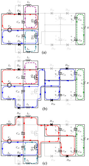
Figure 7.
Equivalent circuits to (a) mode 1: both MOSFETs are ON, (b) mode 2: is ON and is OFF, and (c) mode 3: is OFF and is ON.
2.1. Mode 1: Both MOSFETs Are ON
In this mode, diodes and are forward-biased, and they are ON, which allows the voltage source to charge the inductors and , respectively. Diodes and are reversed biased, and they are OFF. Inductors and are being charged by capacitors and , respectively. All diodes in the VMC stage are reversed biased, and they are OFF. The load is separated from the source, and it is fed by capacitors and . the equivalent circuit for this mode is illustrated in Figure 7a. The inductor voltages are given by
and the output voltage is given by
2.2. Mode 2: Is ON and Is OFF
In this mode, inductor is still being charged by the input source, while is being charged by . Inductors and are discharging to the VMC stage. Diodes and are reversed biased, and diodes and are forward biased. The energy in capacitors and is being discharged, and capacitors and are being charged. The equivalent circuit of this mode is shown in Figure 7b. The state equations are given by
2.3. Mode 3: Is OFF and Is ON
In this mode, and are being discharged to the VMC stage. Diodes and are reversed biased. Diodes and are also reversed biased, and they are OFF. Opposite from mode 2, capacitors and are being discharged, while and are being charged. The equivalent circuit to this mode is shown in Figure 7c. The voltage across the inductors is given by
2.4. Steady-State Analysis and Static Voltage Gain
By applying voltage-second balance to the inductors (using Equations (1)–(4) and (6)–(13)), the voltage across the capacitors and the output voltage, as well as the voltage gain of the converter, can be obtained. The average voltage of the inductors is given by
By solving Equation (14), the voltages of the first stage capacitors can be found, which are given by
Similarly, the voltage across capacitors and is similar to the output capacitor voltage in the quadratic boost converter, which are calculated by
The voltage across capacitors and is twice the voltage across capacitors and , which is calculated by
and the output voltage is calculated by
The voltage gain (M) of the proposed converter with 2 boost stages and 2 VMC cells is
The proposed converter can have more boost stages and VMC cells, as shown in Figure 4. The voltage gain of the proposed converter with k boost converter stages and N VMC cells is given by
Figure 8 shows the voltage gain versus the duty cycles at different numbers of voltage multiplier cells and boost stages. The converter can be fed by two independent voltage sources, and each phase can operate at a different duty cycle. Table 1 shows the output voltage for these cases.
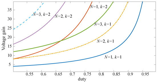
Figure 8.
The voltage gain of the proposed converter with different numbers of boost stages k and voltage multiplier cells N.

Table 1.
Output voltage at different cases when the number of stages are even.
The proposed converter is compared to other topologies in terms of the voltage gain and number of components, as shown in Table 2.
Table 2.
Comparison between different topologies.
3. Components Selection and Efficiency Analysis
3.1. Active Switches
The voltage stress across the MOSFETs are given by
and the maximum current passing through the MOSFETs is given by
where is the switching frequency. The rms currents can be approximated by
3.2. Diodes
The maximum voltage stress across the diodes is given by
The average current and the RMS current passing through the diodes are shown in Table 3.
Table 3.
Diode average and RMS currents.
3.3. Inductors
Inductor selection is based on the required inductance to keep the converter operating safely in the continuous conduction mode (CCM). The input current is given by
the average current passing through inductors and is given by
and the average current passing through inductors and is given by
The operation of the proposed converter in the CCM requires minimum inductance. The minimum inductance for – can be calculated using
The peak and rms currents of all inductors are listed in Table 4.
Table 4.
Inductor peak and RMS currents.
3.4. Capacitors
The voltage across the capacitors is already calculated in. The capacitor values are chosen based on the allowed voltage ripples of the capacitor voltage. The output capacitance is calculated by
The RMS current of the output, and the first stage capacitors are given, respectively, by
3.5. Efficiency Analysis
The efficiency of the proposed converter is mainly affected by the diodes, inductors and MOSFETs. Table 5 lists all the equations used for calculating the losses of the converter. The simulated efficiency is compared to the experimental in Section 4.
Table 5.
Efficiency analysis for components.
4. Experimental Implementation and Results
An 80 W hardware prototype was implemented and tested in the laboratory to verify the operation and the analysis of the converter. Figure 9 shows the hardware prototype, which was implemented using the components listed in Table 6. The was used to supply power at 10 V to the prototype, and the output load was implemented using a mix of ceramic resistors. The duty cycle was set to be around , and that made the output equal to 250 V. The measurements and waveforms were taken at 80 V. Figure 10 shows the voltage waveforms across the switches. The MOSFETs have maximum voltage stress of 62 V. The maximum voltage stress across the diodes in the interleaved single-switch multistage is about 38 V for and and about 63 V for and . The maximum voltage stress across the VMC diodes is 125 V. The voltage across the capacitors, depicted in Figure 11, is 25 V for and , 63 V for and and 125 V for and . The output voltage is about 250 V with ac components of less than . Other waveforms, such as the current of the switches and passive components, are shown in Figure 12 and Figure 13. The converter’s efficiency was simulated and experimentally measured, as shown in Figure 14. The experimental efficiency differs from simulation efficiency by a maximum of . The difference is normal, and it is due to many factors, such as instrument errors and parasitic and conduction losses in the wires and the PCB. The efficiency is about for a load ranges from 20–60 W. The increase of the drawn current from the input source increases the conduction loss of the switching elements and decreases the overall efficiency by at the full load. As mentioned before, the efficiency can be further increased by selecting efficient diodes with low forward voltage for the interleaved boost stage or by replacing the diodes with efficient ones or MOSFETs.
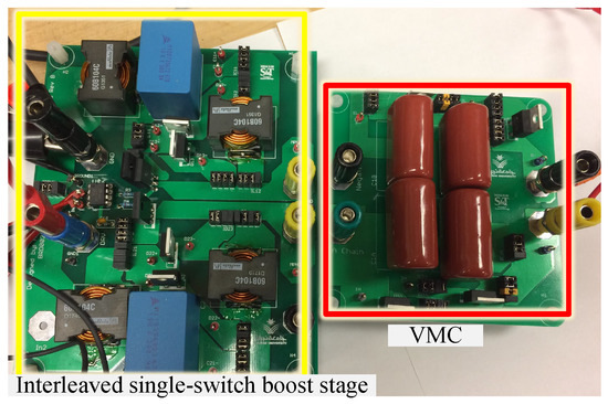
Figure 9.
Hardware prototype.
Table 6.
Component Listing for the Hardware Prototype.
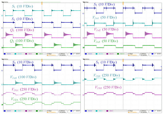
Figure 10.
Voltage waveforms of the MOSFETs and the diodes.
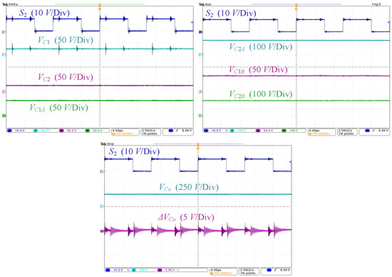
Figure 11.
Voltage waveforms of the capacitors, the output load and the ac components of the output voltage.
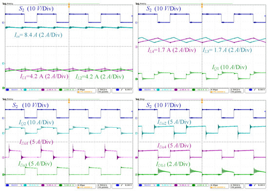
Figure 12.
Current passing through the MOSFETs, inductors and diodes –.
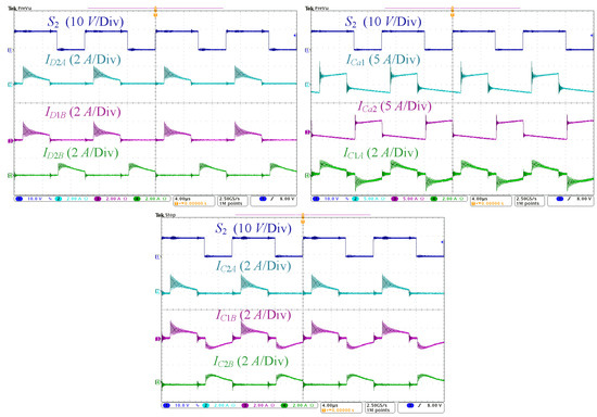
Figure 13.
Currents waveforms of the VMC diodes, VMC capacitors and and .
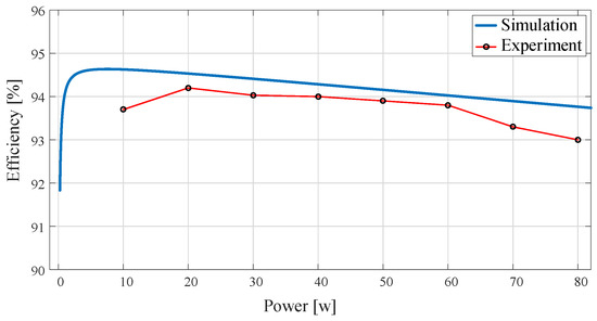
Figure 14.
The efficiency of the hardware prototype and the simulated efficiency.
5. Conclusions
This paper presents a non-isolated interleaved multistage boost converter with VMC. The converter has high voltage and low voltage stresses across the components. Converting a 10 V to a 250 V can be achieved by the quadratic boost stage and a 2-cell VMC when operating at a duty ratio. The converter is capable of converting power from a single source or two independent sources. The input is shared among the two phases equally, and since the converter operates at , the current ripple cancellation is higher than the other interleaved boost converters. The analysis of this converter was explained and validated by simulation and experimental prototype. The converter is very suitable for integrating PV panels to higher-voltage DC buses.
Author Contributions
Conceptualization, A.A., P.S. and M.F.; methodology, M.F. and A.A.; validation, M.F., P.S. and A.A.; formal analysis, A.A.; writing editing, A.A.; supervision, M.F. and P.S. All authors have read and agreed to the published version of the manuscript.
Funding
This research received no external funding.
Acknowledgments
The first author thanks the Najran University for the support.
Conflicts of Interest
The authors declare no conflict of interest.
Abbreviations
The following abbreviations are used in this manuscript:
| VMC | Voltage multiplier cells |
| RMS | Directory of open access journals |
| PCB | Printed circuit board |
| DC | Direct current |
| CCM | Continuous conduction mode |
References
- Wai, R.; Lin, C.; Duan, R.; Chang, Y. High-Efficiency DC-DC Converter With High Voltage Gain and Reduced Switch Stress. IEEE Trans. Ind. Electron. 2007, 54, 354–364. [Google Scholar] [CrossRef]
- Abutbul, O.; Gherlitz, A.; Berkovich, Y.; Ioinovici, A. Step-up switching-mode converter with high voltage gain using a switched-capacitor circuit. IEEE Trans. Circuits Syst. I Fundam. Theory Appl. 2003, 50, 1098–1102. [Google Scholar] [CrossRef]
- Henn, G.A.; Silva, R.; Praca, P.P.; Barreto, L.; Oliveira, D.S., Jr. Interleaved-boost converter with high voltage gain. IEEE Trans. Power Electron. 2010, 25, 2753–2761. [Google Scholar] [CrossRef]
- Lakshmi, M.; Hemamalini, S. Nonisolated High Gain DC–DC Converter for DC Microgrids. IEEE Trans. Ind. Electron. 2018, 65, 1205–1212. [Google Scholar] [CrossRef]
- Carrasco, J.M.; Franquelo, L.G.; Bialasiewicz, J.T.; Galvan, E.; PortilloGuisado, R.C.; Prats, M.A.M.; Leon, J.I.; Moreno-Alfonso, N. Power-Electronic Systems for the Grid Integration of Renewable Energy Sources: A Survey. IEEE Trans. Ind. Electron. 2006, 53, 1002–1016. [Google Scholar] [CrossRef]
- Nordman, B.; Christensen, K. DC Local Power Distribution: Technology, Deployment, and Pathways to Success. IEEE Electrif. Mag. 2016, 4, 29–36. [Google Scholar] [CrossRef]
- Xu, C.; Cheng, K. A survey of distributed power system—AC versus DC distributed power system. In Proceedings of the 2011 4th International Conference on Power Electronics Systems and Applications (PESA), Las Vegas, NV, USA, 12–14 November 2011; pp. 1–12. [Google Scholar]
- Planas, E.; Andreu, J.; Gárate, J.I.; de Alegría, I.M.; Ibarra, E. AC and DC technology in microgrids: A review. Renew. Sustain. Energy Rev. 2015, 43, 726–749. [Google Scholar] [CrossRef]
- Whaite, S.; Grainger, B.; Kwasinski, A. Power quality in DC power distribution systems and microgrids. Energies 2015, 8, 4378–4399. [Google Scholar] [CrossRef]
- Monadi, M.; Zamani, M.A.; Candela, J.I.; Luna, A.; Rodriguez, P. Protection of AC and DC distribution systems Embedding distributed energy resources: A comparative review and analysis. Renew. Sustain. Energy Rev. 2015, 51, 1578–1593. [Google Scholar] [CrossRef]
- Revathi, B.S.; Prabhakar, M. Non isolated high gain DC-DC converter topologies for PV applications–A comprehensive review. Renew. Sustain. Energy Rev. 2016, 66, 920–933. [Google Scholar] [CrossRef]
- Nasir, M.; Khan, H.A.; Hussain, A.; Mateen, L.; Zaffar, N.A. Solar PV-Based Scalable DC Microgrid for Rural Electrification in Developing Regions. IEEE Trans. Sustain. Energy 2018, 9, 390–399. [Google Scholar] [CrossRef]
- Erickson, R.W.; Maksimovic, D. Fundamentals of Power Electronics; Springer: Berlin/Heidelberg, Germany, 2007. [Google Scholar]
- Johnson, S.D.; Witulski, A.F.; Erickson, R.W. Comparison of resonant topologies in high-voltage DC applications. IEEE Trans. Aerosp. Electron. Syst. 1988, 24, 263–274. [Google Scholar] [CrossRef]
- Malik, M.Z.; Chen, H.; Nazir, M.S.; Khan, I.A.; Abdalla, A.N.; Ali, A.; Chen, W. A New Efficient Step-Up Boost Converter with CLD Cell for Electric Vehicle and New Energy Systems. Energies 2020, 13, 1791. [Google Scholar] [CrossRef]
- Rosas-Caro, J.C.; Ramirez, J.M.; Peng, F.Z.; Valderrabano, A. A DC-DC multilevel boost converter. IET Power Electron. 2010, 3, 129–137. [Google Scholar] [CrossRef]
- Walker, G.R.; Sernia, P.C. Cascaded DC-DC converter connection of photovoltaic modules. IEEE Trans. Power Electron. 2004, 19, 1130–1139. [Google Scholar] [CrossRef]
- Leyva-Ramos, J.; Ortiz-Lopez, M.; Diaz-Saldierna, L.; Morales-Saldana, J. Switching regulator using a quadratic boost converter for wide DC conversion ratios. IET Power Electron. 2009, 2, 605–613. [Google Scholar] [CrossRef]
- Kadri, R.; Gaubert, J.; Champenois, G.; Mostefaï, M. Performance analysis of transformless single switch quadratic boost converter for grid connected photovoltaic systems. In Proceedings of the XIX International Conference on Electrical Machines—ICEM 2010, Rome, Italy, 6–8 September 2010; pp. 1–7. [Google Scholar] [CrossRef]
- Ismail, E.H.; Al-Saffar, M.A.; Sabzali, A.J.; Fardoun, A.A. A Family of Single-Switch PWM Converters With High Step-Up Conversion Ratio. IEEE Trans. Circuits Syst. I Regul. Pap. 2008, 55, 1159–1171. [Google Scholar] [CrossRef]
- Luo, F.L.; Ye, H. Advanced DC/DC Converters; CRC Press: Boca Raton, FL, USA, 2016. [Google Scholar]
- Kwon, J.M.; Kwon, B.H.; Nam, K.H. Three-phase photovoltaic system with three-level boosting MPPT control. IEEE Trans. Power Electron. 2008, 23, 2319–2327. [Google Scholar] [CrossRef]
- Yaramasu, V.; Wu, B.; Alepuz, S.; Kouro, S. Predictive control for low-voltage ride-through enhancement of three-level-boost and NPC-converter-based PMSG wind turbine. IEEE Trans. Ind. Electron. 2014, 61, 6832–6843. [Google Scholar] [CrossRef]
- Chub, A.; Vinnikov, D.; Blaabjerg, F.; Peng, F.Z. A Review of Galvanically Isolated Impedance-Source DC-DC Converters. IEEE Trans. Power Electron. 2016, 31, 2808–2828. [Google Scholar] [CrossRef]
- Farakhor, A.; Abapour, M.; Sabahi, M.; Gholami Farkoush, S.; Oh, S.R.; Rhee, S.B. A study on an improved three-winding coupled inductor based dc/dc boost converter with continuous input current. Energies 2020, 13, 1780. [Google Scholar] [CrossRef]
- Barbi, I.; Gules, R. Isolated DC-DC converters with high-output voltage for TWTA telecommunication satellite applications. IEEE Trans. Power Electron. 2003, 18, 975–984. [Google Scholar] [CrossRef]
- Nguyen, M.K.; Lim, Y.C.; Choi, J.H.; Cho, G.B. Isolated High Step-Up DC-DC Converter Based on Quasi-Switched-Boost Network. IEEE Trans. Ind. Electron. 2016, 63, 7553–7562. [Google Scholar] [CrossRef]
- Duarte, J.; Lima, L.; Oliveira, L.; Mezaroba, M.; Michels, L.; Rech, C. Modeling and Digital Control of a Single-Stage Step-Up/Down Isolated PFC Rectifier. IEEE Trans. Ind. Inform. 2013, 9, 1017–1028. [Google Scholar] [CrossRef]
- Evran, F.; Aydemir, M.T. Isolated high step-up DC–DC converter with low voltage stress. IEEE Trans. Power Electron. 2014, 29, 3591–3603. [Google Scholar] [CrossRef]
- Tofoli, F.L.; Pereira, D.; de Paula, W.J.; Oliveira Júnior, D. Survey on non-isolated high-voltage step-up dc-dc topologies based on the boost converter. IET Power Electron. 2015, 8, 2044–2057. [Google Scholar] [CrossRef]
- Forouzesh, M.; Siwakoti, Y.P.; Gorji, S.A.; Blaabjerg, F.; Lehman, B. Step-up DC–DC converters: A comprehensive review of voltage-boosting techniques, topologies, and applications. IEEE Trans. Power Electron. 2017, 32, 9143–9178. [Google Scholar] [CrossRef]
- Li, W.; He, X. Review of Nonisolated High-Step-Up DC/DC Converters in Photovoltaic Grid-Connected Applications. IEEE Trans. Ind. Electron. 2011, 58, 1239–1250. [Google Scholar] [CrossRef]
- Karthikeyan, M.; Elavarasu, R.; Ramesh, P.; Bharatiraja, C.; Sanjeevikumar, P.; Mihet-Popa, L.; Mitolo, M. A Hybridization of Cuk and Boost Converter Using Single Switch with Higher Voltage Gain Compatibility. Energies 2020, 13, 2312. [Google Scholar] [CrossRef]
- Alzahrani, A.; Shamsi, P.; Ferdowsi, M. Boost converter with bipolar Dickson voltage multiplier cells. In Proceedings of the 2017 IEEE 6th International Conference on Renewable Energy Research and Applications (ICRERA), San Diego, CA, USA, 5–8 November 2017; pp. 228–233. [Google Scholar]
- Prabhala, V.A.K.; Fajri, P.; Gouribhatla, V.S.P.; Baddipadiga, B.P.; Ferdowsi, M. A DC–DC Converter With High Voltage Gain and Two Input Boost Stages. IEEE Trans. Power Electron. 2016, 31, 4206–4215. [Google Scholar] [CrossRef]
- Fu, M.; Zhao, C.; Song, J.; Ma, C. A Low-Cost Voltage Equalizer Based on Wireless Power Transfer and a Voltage Multiplier. IEEE Trans. Ind. Electron. 2018, 65, 5487–5496. [Google Scholar] [CrossRef]
- López-Santos, O.; Martínez-Salamero, L.; García, G.; Valderrama-Blavi, H.; Sierra-Polanco, T. Comparison of quadratic boost topologies operating under sliding-mode control. In Proceedings of the Power Electronics Conference (COBEP), Gramado, Brazil, 27–31 October 2013; pp. 66–71. [Google Scholar]
- Li, W.; Lv, X.; Deng, Y.; Liu, J.; He, X. A Review of Non-Isolated High Step-Up DC/DC Converters in Renewable Energy Applications. In Proceedings of the 2009 Twenty-Fourth Annual IEEE Applied Power Electronics Conference and Exposition, Washington, DC, USA, 15–19 February 2009; pp. 364–369. [Google Scholar] [CrossRef]
- Balci, S.; Altin, N.; Komurcugil, H.; Sefa, I. Performance analysis of interleaved quadratic boost converter with coupled inductor for fuel cell applications. In Proceedings of the IECON 2016—42nd Annual Conference of the IEEE Industrial Electronics Society, Florence, Italy, 24–27 October 2016; pp. 3541–3546. [Google Scholar] [CrossRef]
Publisher’s Note: MDPI stays neutral with regard to jurisdictional claims in published maps and institutional affiliations. |
© 2020 by the authors. Licensee MDPI, Basel, Switzerland. This article is an open access article distributed under the terms and conditions of the Creative Commons Attribution (CC BY) license (http://creativecommons.org/licenses/by/4.0/).