Abstract
A Single-Ended Primary-Inductor Converter (SEPIC) converter with an Inductor-Capacitor (LC) regenerative snubber is proposed to reduce Electromagnetic Interference (EMI) for Electric Vehicle (EV) applications. The switching energy is transferred through a capacitor to an inductor which is coupled to SEPIC inductors. This technique reduces the number of components and also returns some of switching energy to SEPIC converter. The mathematical analysis and optimization of LC snubber with respect to number of turns is also presented. Spice simulations and experimental results are provided to verify its performance. The proposed LC regenerative snubber reduces the peak voltage by 16 V on the switching transistor during the switching transient. It is also indicated that 8 dB reduction is achieved in the EMI measurements at ringing frequency and 10 dB reduction at high frequency band.
1. Introduction
Over the past decades, research has been directed towards EV to improve the environmental conditions [1]. EV systems depend on electric power as its energy source rather than the fuel like in conventional vehicle systems. The main components of the EV system are battery for energy storage, motor for traction, AC/DC converter to charge the battery and supply energy to the motor from the battery, and DC/DC converter to provide energy to the low-power components in the EV system. The current use of DC/DC converters with transformers or coupled inductors causes the following problems in the EV system; high voltage stress across the the power switch, increasing the converter area, and increasing the EMI [2]. To design a DC/DC converter for an EV system, there are some constraints that should be considered: high efficiency, small volume, and low EMI [3]. Several typologies of DC/DC converters are used in EV applications such as Buck converter, Boost converter, Buck-boost converter, and SEPIC converter.
SEPIC is considered a buck-boost DC/DC converter. It differs from the regular buck-boost converter such that the output voltage polarity in the SEPIC converter is non-inverting [4]. SEPIC converter is designed using two separate inductors [5]. However, using two coupled inductors rather than two separated inductors reduces the required inductance for the same inductor ripple current in half [6,7]. SEPIC converter with two coupled inductors is shown in Figure 1, where and are the coupled inductors. Like most of the other DC/DC converters which contain a coupled inductors or transformer in their circuit, SEPIC converter suffers from the energy stored in the leakage inductance of the primary inductor. This energy causes a voltage stress on the switch transistor during the turn OFF period and may damage the Metal–Oxide Field–Effect Transistor (MOSFET) switch [8]. To prevent that damage, a snubber circuit is used to create an alternative path for that energy and protect the MOSFET switch. Besides that, the ringing created from the resonance between the leakage inductance of the primary inductor and the parasitic capacitance of the MOSFET switch, increases the EMI of the converter at the ringing frequency [9]. In addition, to protect the switch from the energy stored in the leakage inductance, snubber circuit reduces the EMI as presented in [10,11].
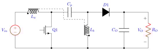
Figure 1.
Single-Ended Primary-Inductor Converter (SEPIC) converter with coupled inductors.
Snubber circuits are classified as dissipative and non-dissipative. The most commonly used dissipative snubber is the Resistor-Capacitor (RC) snubber. It consists of a capacitor and a resistor in series connected in parallel with the transistor [12]. In this type of snubber, during the turn OFF period, the stored energy in the leakage inductance is transferred to the snubber capacitor through the snubber resistor. In the turn ON period, the snubber capacitor discharges that energy through the transistor. Another dissipative snubber is the Resistor-Capacitor-Diode (RCD) snubber, which differs from the RC snubber by containing a diode in parallel with the resistor. The operation of the RCD snubber is the same as the RC snubber operation, except in the RCD snubber during the turn OFF period, the energy is transferred to the capacitor through the diode not through the resistor [13]. There is a trade off between the RC and the RCD snubbers. The RCD snubber decreases the power loss during the turn OFF period compared to the RC snubber. However, the RC snubber achieves more suppression for the over-voltage peak during the turn OFF period [14]. Connecting the snubber circuit in parallel with the MOSFET switch causes more current stress on it [13]. By connecting the snubber circuit in parallel with the primary inductor rather than the MOSFET switch, the current stress on the MOSFET switch is avoided [15]. The performance of the snubber circuit does not change by connecting it in parallel with the primary inductor. A SEPIC converter with RCD snubber is shown in Figure 2a.
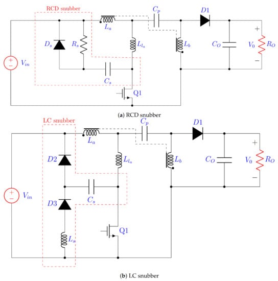
Figure 2.
SEPIC converter with a (a) RCD snubber and (b) LC snubber.
A non-dissipative LC snubber is presented for flyback converter in [16]. The snubber action is analyzed for four different operation modes. These modes differ from each other by when the energy stored in the snubber capacitor is returned to the supply. In mode 1, no energy is returned to the supply after stored it in the snubber capacitor during the turn OFF period. During the turn ON period, the snubber capacitor is discharged through the snubber inductor and the transistor. In mode 2, the energy in the snubber capacitor is returned to the supply during the turn ON period. In mode 3, the energy is returned to the supply during the turn ON and the turn OFF periods. In mode 4, the energy is returned to the supply in the turn OFF period. The voltage across the snubber capacitor determines in which mode the snubber operates.
The LC snubber has an advantage over the RC snubber, because it is able to return the stored energy in the leakage inductance through the snubber inductor to the supply rather than dissipating it like the RC snubber. On the other hand, an extra inductor used in this type of snubber increases the number of components. A SEPIC converter with an LC snubber is shown in Figure 2b.
The regenerative snubber for flyback converter presented in [17,18] differs from the LC snubber, because it is based on three coupled inductors rather than the regular two coupled inductors or two winding transformer. The third coupled inductor or the auxiliary inductor is used as a snubber inductor instead of using a separate inductor like LC snubber. That reduces the number of required components and transfers the energy also to the secondary side during the turn ON period.
In this paper, a coupled inductor based LC regenerative snubber for SEPIC converter is proposed to minimize the switching stress on the transistor, as shown in Figure 3. This method also reduces the Electromagnetic Interference (EMI) which occurs due to the switching activity. The rest of the paper is organized as follows. The operation of a SEPIC converter with regenerative snubber is analyzed and design constraints for the snubber component values are determined in Section 2. In Section 3, the advantages of regenerative snubber for SEPIC converter are verified by simulation and experimental results. Finally, a conclusion about the results of using the regenerative snubber for SEPIC converter is presented in Section 4.
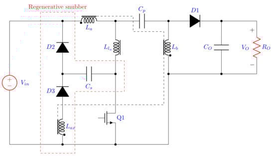
Figure 3.
SEPIC converter with regenerative snubber.
2. Analysis of LC Regenerative Snubber for SEPIC Converter
For the SEPIC converter with regenerative snubber shown in Figure 3, there are four states in each operation cycle, as shown in Figure 4. Two of these states are in , which is the turn ON period, and the other two states are in , which is the turn OFF period. The snubber circuit is active at the first state of the turn ON period from to , and at the first state of the turn OFF period from to . At the second state of the turn ON period from to and at the second state of the turn OFF period from to , the SEPIC converter acts like a regular SEPIC converter without any effects from the snubber circuit. In analyses, voltage drops across diodes and transistor are neglected. The leakage inductance at the primary side and at the auxiliary winding are taken into account.
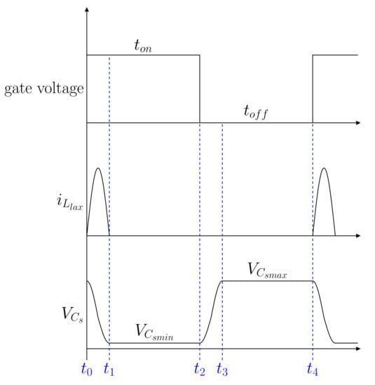
Figure 4.
Waveforms for gate voltage, and .
2.1. Operating State of LC Snubber Circuit
As shown in Figure 4 , the first state of the turn ON period starts at when the MOSFET switch is turned on. In this state, and are off, is on, and the voltage across is which is the maximum voltage. During this state, discharges through the MOSFET switch and , where is the auxiliary inductor. In this state, as presented in [18] for the flyback converter, the voltage across the auxiliary inductor is equal to the reflected voltage from the primary inductor only. However, in the SEPIC converter, the voltage across is equal to the reflected voltage from the primary and the secondary inductors, this is one of the main differences between the regenerative snubber performance in the SEPIC and in the flyback converters. This state ends at , when becomes off and the current through becomes zero. The equivalent circuit of the SEPIC with regenerative snubber in this state is shown in Figure 5a. The equivalent circuit for the snubber circuit is shown in Figure 5b, where is the leakage inductance at the auxiliary side and is the voltage across .
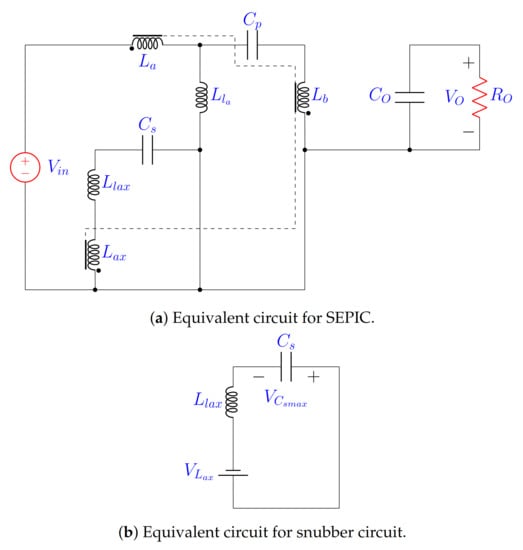
Figure 5.
Equivalent circuit at the first state in the turn ON period for SEPIC and snubber circuit.
is the leakage inductance at the primary side, is the number of turns for , is the number of turns for the primary side , and is the number of turns for the secondary side . Suppose that the SEPIC is designed to have , the voltage of the leakage inductance at the auxiliary side is obtained as
The time constant for the equivalent circuit in Figure 5b is
The impedance of the leakage inductance is
The current through equals to
The voltage across equals to
when , reaches . As shown in (6) and Figure 4, when , by substituting that in (7)
The power consumption in during this state is
where is the average current of during this state. is the voltage drop across D3. equals to
where T is the switching time. After turns off at , the second state in the turn ON period begins. In this state, the snubber circuit does not affect the performance of the SEPIC and the converter acts like regular SEPIC in the turn ON period until the turn OFF period starts at when the MOSFET switch is turned off.
At the first state of the turn OFF period, the snubber is active. In this state, and are on, and is off. The equivalent circuit for the SEPIC converter and for the snubber circuit in this state are shown in Figure 6a,b, respectively. is the reflected voltage from the secondary side to the primary side and it is equal to . The voltage across at the beginning of this state is . This state ends at when reaches , that happens when the current through the leakage inductance .
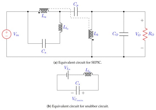
Figure 6.
Equivalent circuit at the first state in the turn OFF period for SEPIC and snubber circuit.
The time constant for the equivalent circuit in Figure 6b is
The impedance of the leakage inductance is
The current through the leakage inductance equals to
where I is the peak of the magnetizing current. Suppose that is selected to have , the current through the leakage inductance is written as
The voltage across equals to
From (15), reaches at and it equals to
The power consumption in during this state is
where is the average current of during this state. is the voltage drop across . equals to
After the current through the leakage inductance becomes zero at , turns off and the second state of the turn OFF period starts. During the steady state of this period, charges to the input voltage . This leads to that the voltage across MOSFET during this period equals to the summation of the input voltage and the output voltage. In this state, the converter acts like regular SEPIC converter in the turn OFF period without any effects from the snubber circuit until when the MOSFET switch is turned on again. All of these states are repeated in each cycle.
2.2. Components Sizing
During the first state of the turn ON period, drops to , after that turns off. Moreover, during the turn OFF period to make on, should be greater than [18]. From that, and by solving the following inequality,
Moreover, as mentioned in Section 2 that should be selected to have , by solving the following inequality taking (20) into consideration and using (17),
where D is the duty cycle. In the first state of the turn ON period, reaches when , which means half of the time constant. This should happen within the turn ON period, this leads to
By using (22) and (24), the upper and lower limits for are determined. Moreover, by using (28) and (30), the upper and lower limits for are obtained. From the previous constraints, the value of the leakage inductance of the primary is very critical and important to determine the limits of and . To calculate the leakage inductance value, the value of the parasitic capacitance of the switch should be known. If it is not known, to calculate it, the frequency of the ringing should be measured. It equals to
where is the parasitic capacitance. After measuring the ringing frequency, an additional capacitor should be connected in parallel with the parasitic capacitance and then new ringing frequency should be measured. The new frequency equals to
where is the additional capacitor. By using (31) and (32), the parasitic capacitance is calculated and it equals to
After calculating , the leakage inductance is calculated by rearranging (31)
3. Simulation and Experimental Results
LTSpice is used to simulate the SEPIC converter with regenerative snubber. Component parameters used in the simulation are shown in Table 1. The simulation setup is shown in Figure 7.

Table 1.
Simulation and experimental parameters.
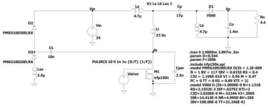
Figure 7.
Simulation setup for SEPIC converter.
From the design constraints illustrated in the Section 2, the values of and are related to each other. From (22), the lower limit for is
By drawing (24) using the above constraint for the lower limit of as shown in Figure 8, the chosen pair of and values should be under the graph. To avoid the sensitive areas, the optimum values of and are found to be in the area under the graph and bounded by 25 nF and 6.5. The chosen pair for (,) is (10 nF, 5).
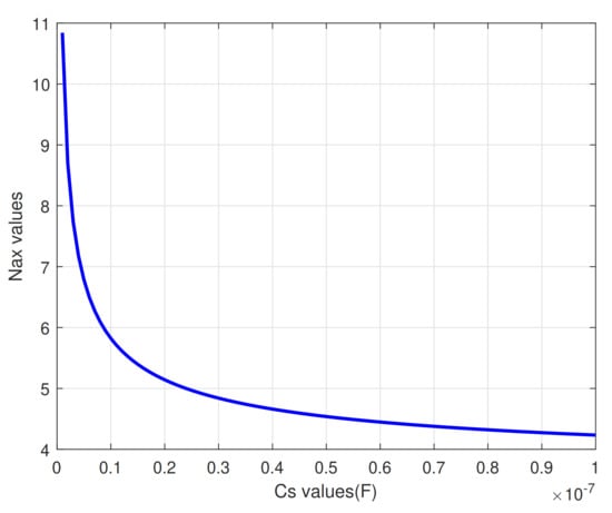
Figure 8.
Values of and .
The simulation results of the voltage across the MOSFET switch of the SEPIC converter without regenerative snubber and with non-coupled and coupled regenerative snubber for 24 V are shown in Figure 9. To ensure that the regenerative snubber has the same effect on the SEPIC converter with different values of , the voltage across the MOSFET switch without snubber and with snubber for 28 V and 22 V are depicted in Figure 10 and Figure 11, respectively. Without coupling of snubber inductance to SEPIC inductors, the improvement is limited, as shown in Figure 9b, Figure 10b, and Figure 11b. The coupling between snubber inductance and SEPIC inductors contribute significant reduction of ringing, as shown in Figure 9c, Figure 10c, and Figure 11c. Comparison between simulation results is shown in Table 2 where Avg. P is the average power consumption in the MOSFET during turn OFF period, D is the duty cycle, is the voltage overshoot across the MOSFET, and is the steady-state voltage across the MOSFET during turn OFF period. Using the regenerative snubber, the average power consumption in the MOSFET, the overshoot voltage during the turn OFF period and the required time to reach the steady state are all reduced.
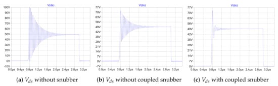
Figure 9.
Simulation results for the voltage across the MOSFET switch “ 24 V”.
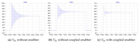
Figure 10.
Simulation results for the voltage across the MOSFET switch “ 28 V”.
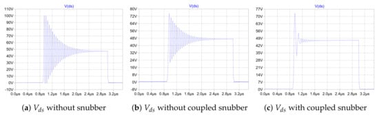
Figure 11.
Simulation results for the voltage across the MOSFET switch “ 22 V”.
Table 2.
Simulation results comparison.
For the experiment, a prototype for SEPIC converter is built, as shown in Figure 12. The voltage across the MOSFET switch in the turn OFF period without the regenerative snubber and with the regenerative snubber experimentally for 24 V are shown in Figure 13a,b, respectively. The regenerative snubber reduces the stress on the switch by reducing the ringing and suppressing the voltage surge by 16 V. Moreover, the voltage across the MOSFET switch of the SEPIC during the turn OFF period with snubber and without snubber for different input voltages are shown in Figure 14 and Figure 15, respectively. The voltage on the MOSFET switch without coupled inductance in the regenerative snubber is shown in Figure 16b. Although the peak voltage is reduced compared to the one without snubber circuit, the time for settling due to the ringing does not change significantly.
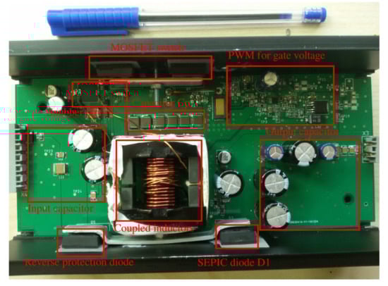
Figure 12.
Prototype for SEPIC converter.
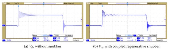
Figure 13.
Experimental results for the voltage across the MOSFET switch “ 24 V”.
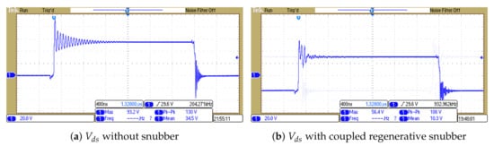
Figure 14.
Experimental results for the voltage across the MOSFET switch “ 28 V”.
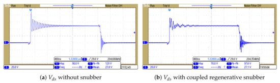
Figure 15.
Experimental results for the voltage across the MOSFET switch “ 22 V”.
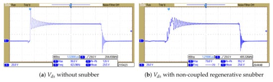
Figure 16.
Experimental results for the voltage across the MOSFET switch “ 24 V”.
Reverse protection diode and SEPIC diode are selected as PN junction diode. Although PN junction diode has higher forward voltage drop than a schottky diode, it has lower reverse current leakage at high temperature. The voltage drop on these diodes is around 0.9 V. Therefore, for a 4.4 load these diodes contribute 11 W of power loss. The ferrite core is based on N87 material and has 4 W of power loss. The power loss due to the series resistance of inductors is 1 W. The conduction and switching losses of the MOSFET switches are 1 W and 3 W, respectively. The gate driver circuit including its low-dropout regulator contributes 1.5 W of power loss. The rest of the circuit contributes less than 0.5 W. Therefore, for 4.4 load the output power is 131 W and total power loss is 22 W. This results in 85 % efficiency. Since snubber circuit improves switching losses which is only 14 % of the total loss, the effect of snubber circuit on the efficiency is limited.
To measure EMI for the SEPIC converter, Rohde & Schwarz FSH8 spectrum analyzer is used. The SEPIC converter without regenerative snubber has a peak at the ringing frequency which is 20 MHz, as shown in Figure 17a. After using the regenerative snubber as shown in Figure 17b, the peak at the ringing frequency is suppressed by 8 dB. On the other hand, another peak appears at 29.75 MHz, but still less than the peak without regenerative snubber by 2.8 dB.
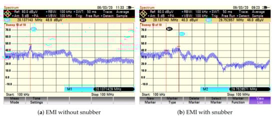
Figure 17.
EMI for the SEPIC converter “ 24 V”.
The EMI for the SEPIC without regenerative snubber and with regenerative snubber for input voltage 28 V and 22 V are shown in Figure 18 and Figure 19, respectively. For 28 V as shown in Figure 18a, the converter has a peak of 48.6 dB at the ringing frequency. In Figure 18b, using the regenerative snubber reduces that peak to 40 dB. Moreover, at high frequency, the EMI is reduced by 10 dB. The same thing happens for 22 V, as shown in Figure 19, where the converter has a peak of 50.4 dB at the ringing frequency. Using the regenerative snubber reduces the peak at the ringing frequency to 42.3 dB. Moreover, EMI at high frequency is reduced by 10 dB. EMI for SEPIC with non-coupled regenerative snubber is shown in Figure 20 which does not reduce the EMI compared to the coupled regenerative snubber. Performance measurement results with regenerative snubber and without regenerative snubber for different input voltages 24 V, 28 V, and 22 V and with non-coupled regenerative snubber for 24 V are summarized in Table 3.
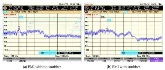
Figure 18.
EMI for the SEPIC converter “ 28 V”.
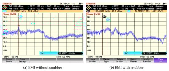
Figure 19.
EMI for the SEPIC converter “ 22 V”.
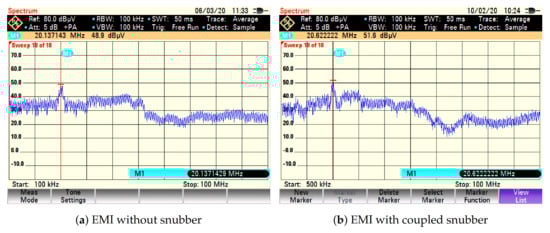
Figure 20.
EMI for the SEPIC converter “ 24 V”.
Table 3.
Performance measurement results.
4. Conclusions
An LC regenerative snubber for SEPIC converter for EV applications is proposed. The operation of the SEPIC converter with regenerative snubber is analyzed. Determination and sizing for the components of the regenerative snubber are presented. The effects of using the proposed snubber on the SEPIC are verified by simulation and experimental results. The peak of the voltage stress on MOSFET switch of the SEPIC converter is reduced by 16 V. An improvement on the EMI performance of the SEPIC converter is achieved by 8 dB reduction at the ringing frequency. Moreover, EMI is reduced at high frequencies by 10 dB. Using the proposed snubber does not affect the efficiency of the SEPIC. The values of the snubber capacitor and inductor are sensitive, they should be selected to have enough margin not to be affected by the parasitic capacitance and the leakage inductance values.
Author Contributions
A.K. contributed software and hardware development, writing—original draft preparation; B.K. conceived the idea of the research, supervised this research study, and participated in all of the study phases; S.B.O. and A.A. contributed in analyzing the results and improved the structure of the paper; O.H. reviewed the results and edited the manuscript. All authors have contributed significantly to this work. All authors have read and agreed to the published version of the manuscript.
Funding
This work was partially supported by The Scientific and Technological Research Council of Turkey (TUBITAK) (grant 5170021).
Acknowledgments
Authors acknowledge Flanders Make for the support of this research study.
Conflicts of Interest
The authors declare no conflict of interest.
References
- Naunin, D. Electric Vehicles. In Proceedings of the IEEE International Symposium on Industrial Electronics, Warsaw, Poland, 17 June 1996; pp. 11–24. [Google Scholar] [CrossRef]
- Bellur, D.M.; Kazimierczuk, M.K. DC-DC Converters for Electric Vehicle Applications. In Proceedings of the 2007 Electrical Insulation Conference and Electrical Manufacturing Expo, Nashville, TN, USA, 22–24 October 2007; pp. 286–293. [Google Scholar] [CrossRef]
- Sakka, M.A.; Mierlo, J.V.; Gualous, H. Electric Vehicles—Modelling and Simulations; Soylu, S., Ed.; IntechOpen Limited: London, UK, 2011; Chapter 13; ISBN 978-953-307-477-1. [Google Scholar] [CrossRef]
- Ridley, R. Analyzing the SEPIC Converter; Power Systems Design: St. Annapolis, MD, USA, 2006; pp. 14–18. [Google Scholar]
- de Melo, P.F.; Gules, R.; Romaneli, E.F.R.; Annunziato, R.C. A Modified SEPIC Converter for High-Power-Factor Rectifier and Universal Input Voltage Applications. IEEE Trans. Power Electron. 2010, 25, 310–321. [Google Scholar] [CrossRef]
- Falin, J. Designing DC/DC converters based on SEPIC topology. Analog Appl. J. 2008, 4Q, 18–23. [Google Scholar]
- Betten, J. Benefits of a coupled-inductor SEPIC converter. Analog Appl. J. 2011, 2Q, 14–17. [Google Scholar]
- Erickson, R.W.; Maksimovic, D. Fundamentals of Power Electronics, 2nd ed.; Springer: New York, NY, USA, 2001; ISBN 978-1-4757-0559-1. [Google Scholar] [CrossRef]
- Dutta, A.; Ang, S.S. Effects of parasitic parameters on electromagnetic interference of power electronic modules. In Proceedings of the 2017 IEEE Applied Power Electronics Conference and Exposition (APEC), Tampa, FL, USA, 26–30 March 2017; pp. 2706–2710. [Google Scholar] [CrossRef]
- Yuvarajan, S.; Nelson, R.; Quek, D. A study of the effects of snubber on switching loss and EMI in an MCT converter. In Proceedings of the 1994 IEEE Industry Applications Society Annual Meeting, Denver, CO, USA, 2–6 October 1994; pp. 1344–1349. [Google Scholar]
- U-Yaisom, C.; Khanngern, W.; Nitta, S. The study and analysis of the conducted EMI suppression on power MOSFET using passive snubber circuits. In Proceedings of the 3rd International Symposium on Electromagnetic Compatibility, Beijing, China, 21–24 May 2002; pp. 561–564. [Google Scholar] [CrossRef]
- Yatsugi, K.; Nomura, K.; Hattori, Y. Analytical Technique for Designing an RC Snubber Circuit for Ringing Suppression in a Phase-Leg Configuration. IEEE Trans. Power Electron. 2018, 33, 4736–4745. [Google Scholar] [CrossRef]
- Liu, S.; Lin, H.; Wang, T. Comparative Study of Three Different Passive Snubber Circuits for SiC Power MOSFETs. In Proceedings of the 2019 IEEE Applied Power Electronics Conference and Exposition (APEC), Anaheim, CA, USA, 17–21 March 2019; pp. 354–358. [Google Scholar] [CrossRef]
- Wu, Y.; Yi, Q.; Wu, Y.; Yang, F.; Zhang, Z.; Wen, J. Research on Snubber Circuits for Power Electronic Switch in DC Current Breaking. In Proceedings of the 2019 14th IEEE Conference on Industrial Electronics and Applications (ICIEA), Xi’an, China, 19–21 June 2019; pp. 2082–2086. [Google Scholar] [CrossRef]
- Hren, A.; Korelic, J.; Milanovic, M. RC-RCD clamp circuit for ringing losses reduction in a flyback converter. IEEE Trans. Circuits Syst. II Express Briefs 2006, 53, 369–373. [Google Scholar] [CrossRef]
- Domb, M.; Redl, R.; Sokal, N.O. Nondissipative turn-off snubber alleviates switching power dissipation, second-breakdown stress and VCE overshoot: Analysis, design procedure and experimental verification. In Proceedings of the 1982 IEEE Power Electronics Specialists Conference, Cambridge, MA, USA, 14–17 June 1982; pp. 445–454. [Google Scholar] [CrossRef]
- Ai, T.-H. A Novel Integrated Nondissipative Snubber for Flyback Converter. In Proceedings of the IEEE ICSS 2005 International Conference on Systems & Signals, Kaohsiung, Taiwan, 28–29 April 2005; pp. 66–71. [Google Scholar]
- Liao, C.-S.; Smedley, K.M. Design of High Efficiency Flyback Converter with Energy Regenerative Snubber. In Proceedings of the 2008 Twenty-Third Annual IEEE Applied Power Electronics Conference and Exposition, Austin, TX, USA, 24–28 February 2008; pp. 796–800. [Google Scholar] [CrossRef]


Publisher’s Note: MDPI stays neutral with regard to jurisdictional claims in published maps and institutional affiliations. |
© 2020 by the authors. Licensee MDPI, Basel, Switzerland. This article is an open access article distributed under the terms and conditions of the Creative Commons Attribution (CC BY) license (http://creativecommons.org/licenses/by/4.0/).