Abstract
Three-phase, four-wire split capacitor inverters are currently employed in many applications, such as photovoltaic systems, battery chargers for electric vehicles, active power filters, and, in general, in all grid-tied applications that deal with possible grid voltage and/or current unbalances. This paper provides a comprehensive evaluation of the capacitor-switching voltage ripple and dc-link switching voltage ripple for the three-phase, four-wire, split capacitor inverters. Specifically, analytical formulations of the peak-to-peak and rms values of the voltage ripples are originally pointed out in this paper and determined in the case of balanced three-phase and unbalanced (two-phase and single-phase) output (ac) currents. The obtained results can help in designing the considered inverter and sizing of the dc-link capacitors. Reference is made to the sinusoidal PWM modulation and sinusoidal three-phase output currents with an almost unity power factor, representing a grid-connected application. Extensive numerical simulations have been carried out to thoroughly verify all the analytical developments presented in this paper. Furthermore, some experimental tests, having balanced output currents on the ac side, have been accomplished, validating numerical simulations and analytical developments.
1. Introduction
Three-phase, four-wire, voltage-source inverters (VSIs) are employed in different power electronic applications, mainly involving unbalanced loads. They are currently adopted in grid-forming inverters [1], electric drives [2], active rectifiers [3], and shunt active filter [4] applications due to their inherent ability to deal with the zero-sequence voltage and current components. Another emerging application for this kind of topology is electric vehicle (EV) battery chargers, owing to the expansion of electric vehicles (EVs) on the world’s roads. Three-phase, four-wire inverters can be used as active front-end rectifiers of double-stage EV battery chargers enabling vehicle-to-grid (V2G), vehicle-for-grid (V4G), and vehicle-to-X (V2X) services [5]. Many different topologies have been recently proposed in the literature, such as four-leg with [6] and without [7,8,9] neutral inductor, independently controlled neutral module [10], and four-wire, split capacitor arrangement with [11] and without [1] neutral inductor. Among the wide variety of available modulation schemes, carrier-based PWM techniques are extensively adopted due to their simplicity, well-known harmonic spectrum, and fixed switching frequency. The latter aspect makes evaluation of the converter switching losses easy and, therefore, the converter design is more accurate [12]. In [13], the dc-link voltage ripple and the dc-link capacitor design for a single-phase inverter were presented.
Many studies have been reported in the literature on three-phase voltage-source inverters [13,14,15,16]. In [14], the dc-link voltage ripple caused by unequal instantaneous power was analyzed for two different modulation methods in the case of two-level three-phase inverter, and the power loss of dc-link was estimated based on the ESR and rms current of the dc-link capacitor. Several commercial capacitor technologies, under consideration for use as dc bus capacitors for electric vehicle traction inverters, were reviewed and evaluated in [15] for their ability to optimize the volume of traction inverters. An optimal switching period phase-shifted method for a slave inverter to reduce grid current ripples in synchronized two parallel three-phase grid-connected voltage-source inverters (VSI) was presented in [16].
The analysis was extended to a three-phase, three-level flying capacitor inverter and neutral point clamped (NPC) converter in [17] and [18], respectively. The rms current, through dc-link capacitors, was analytically evaluated in a three-level NPC inverter in [19]. Based on the dc-link voltage analysis and considering both low- and/or high-frequency voltage components, simple and effective guidelines for designing the dc-link capacitor were presented in [20] for a three-phase two-level inverter.
Major attention has been paid to the inverters’ output voltage and current characteristics. Although the dc side of the converters was widely investigated as well, a few analytical developments were presented investigating the dc voltage switching ripple under balanced and unbalanced ac current conditions. It is well known that the accurate selection of the dc-link capacitors, where present, is crucial. These components can be a source of failure in the inverter, and they directly impact the price and the lifetime of the system. Therefore, they should be correctly designed and sized, and a proper analysis of the inverter dc-link input current and voltage is essential. The dc-link capacitors must handle inverter input current harmonics and avoid high voltage ripples.
Considering three-phase, four-wire, split capacitor inverters, the dc-link switching voltage ripple in three-phase four-wire split-capacitor inverters has not been examined in the existing literature to date. A model-based controller for a three-phase four-wire shunt active filter, which uses a three-leg split-capacitor topology to implement the voltage source inverter, is presented in [21]. The most popular topologies applied to four-wire systems have been studied and analyzed in [22] in terms of ratings of dc-link voltage and current, and the quality and efficiency of output waveforms. In [6] and [23], a relation of the dc-link voltage ripple with respect to low-order harmonics was derived. However, the rms value was not evaluated, and a complete analysis is not given. In [1], the dc-bus voltage oscillation and the output voltage total harmonics distortion (THD) at imbalanced load were calculated for a three-phase inverter with split dc-link capacitors. The study showed positive, negative, and zero voltage components and only low harmonic voltage was considered. In [24], the peak value of a low-harmonics voltage ripple across the dc-link capacitor in case of an unbalanced load in the inverter is given. The authors in [25] also conducted a low harmonic analysis for the dc-link voltage ripple, and a design of the dc-link capacitors was done in terms of peak-to-peak voltage low-harmonic oscillations. However, in these works, only the low-frequency voltage ripple component was considered. Although the latter is the dominant contribution to the dc-link capacitor voltage ripple, it is not the only one, and the switching voltage ripple should be also considered for a proper design of the dc-link capacitors.
Examining a three-phase, four-wire, split capacitor inverter, in this paper, a comprehensive dc-link voltage ripple analysis with respect to switching frequency is provided for the individual capacitor voltages and total dc-link voltage. Analytical formulations of the peak-to-peak and rms voltage ripple are originally pointed out in this paper. The obtained results can help in designing the considered three-phase inverter, with reference to the sizing of the dc-link capacitors. A balanced sinusoidal PWM (SPWM) was applied to the inverter, while the load parameters were selected to achieve almost sinusoidal load currents with a unity power factor. The characteristics of the dc-link voltage ripple are examined with reference to both balanced three-phase and unbalanced (two-phase and single-phase) ac currents. These three study cases were selected as extreme operating conditions, while the other, intermediate modes can be easily derived from the presented examples. Numerical simulations are provided to verify the analytical developments. Some experimental tests were also conducted, considering balanced, three-phase output currents.
The paper is formed by six sections. The system configuration and modulation principle are presented in Section 2. The inverter’s input current ripple is evaluated in case of balanced and unbalanced output load currents, and the voltage ripple across both the individual capacitors and total dc-link are provided in Section 3 and Section 4, respectively. Section 5 presents the experimental results and, finally, conclusions are drawn in Section 6.
2. System Configuration and Modulation Principle
The considered circuit scheme is illustrated in Figure 1. It consists of a three-phase, four-wire, split capacitor inverter supplying currents ia, ib and ic, which are sinusoidal (the corresponding switching ripple is neglected). The inverter is supplied by a dc voltage source (Vdc) via a dc source impedance representing an inductive filter (Ldc) and/or an equivalent series resistance (Rdc).
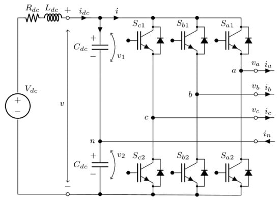
Figure 1.
Circuit scheme of a three-phase, four-wire, split capacitor VSI.
In case of balanced modulation (Va = Vb = Vc = V = mVdc), the three modulating signals are given by the sinusoidal phase reference voltages normalized with Vdc
being ϑ phase angle (ϑ = ωt), fundamental (grid) angular frequency and m modulation index ranges between 0 and 0.5 (0 ≤ m ≤ 0.5).
Considering Equation (1), and neglecting the output current ripple, the corresponding three-phase output currents are
where Ia, Ib and Ic are the output current amplitudes of phases a, b and c, respectively, and φ is the phase angle between corresponding phase voltage and current. Having a load with a unity power factor, Equation (2) can be rewritten in terms of positive sequence I+, negative sequence I−, and zero sequence I0 as
where β− and β0 are the phase angles of the negative and zero sequences of the current, respectively.
3. Evaluation of Inverter Input Current Ripple for Balanced and Unbalanced Loads
With regard to Figure 1, the inverter input current is the sum of currents that flow through each inverters’ legs, and it can be calculated based on the switching function of each upper leg switch and the corresponding output current as
The switching functions Sa1, Sb1, Sc1 are characteristic functions that obtain value 1 when the corresponding switch is turned ON, and 0 if the switch is turned OFF.
As an alternative, the inverter input current of Equation (4) can be rewritten as
where Idc is the dc (average) component; is the low-frequency part; is the high-frequency (switching) constituent and, finally, is the averaged input current over a switching period, which is composed of dc (average) and low-frequency components.
The averaged input current can be calculated as
Replacing Equations (1) and (2) into Equation (6) leads to the following low-frequency and dc components
3.1. Balanced Load
Having a unity power factor load, when the load is balanced (Ia = Ib = Ic = I), the low-frequency component described by Equation (7) is zero. Consequently, the instantaneous inverter input current contains only the switching-frequency component and the dc (average) Idc given by
Figure 2 shows the simulation results, comparing the instantaneous input current (blue trace) with its averaged value over the switching period (red trace), and the corresponding average current component calculated by Equation (9) (green trace) in the case of m = 0.4.
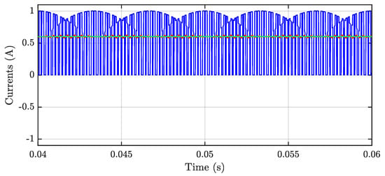
Figure 2.
Instantaneous input current: (blue), its averaged value over the switching period (red), and calculated value (green) in case of balanced output currents for m = 0.4, I = 1A and φ = 0°.
In the case of balanced output currents, the analysis can be limited to one-sixth of a fundamental period (T/6) thanks to the symmetry of the input current, shown in Figure 2. A perfect match of averaged value of the input dc current with an analogue that has been theoretically determined by Equation (9) can be observed in Figure 2. As can be seen, a small delay between averaged and theoretical currents (Tsw/2) is due to the averaging process itself.
3.2. Unbalanced Load—Only Two Phases (Phases a and b)
In the case of unbalanced load with only two phases working, the averaged input current can be written as
Similarly, the averaged input current can be calculated for other combinations of the phases.
If the current amplitudes of the two operating phases are equal (Ia = Ib = I, Ic = 0), while phase angle displacement is preserved unchanged, the instantaneous inverter current, together with its averaged counterpart, are depicted in Figure 3. The initial conditions for this example are the following: the load with unity power factor (φ = 0°) and m = 0.4. A good correlation among analytical and numerical results could be noticed. The small phase mismatch is introduced due to the moving average filtering.
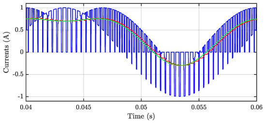
Figure 3.
Input current: instantaneous value (blue), its averaged value over the switching period (red), and calculated value (green) in case of unbalanced two phases for m = 0.4, Ia = Ib = I = 1 A and φ = 0°.
3.3. Unbalanced Load—A Single-Phase Load (Phase a)
In this case study, the averaged inverter input current is
Similarly, the averaged input current can be calculated for the other phases, b and c.
Figure 4 displays a comparison between simulation results of the instantaneous, input dc current (blue trace) along with its averaged value over a switching period (red trace) and waveform given by Equation (11) (green trace). The initial conditions that were applied in this simulation are identical to the previous study cases, namely m = 0.4 and φ = 0°. Again, a good equivalence of the numerical and theoretical profiles can be observed. A small delay between averaged and theoretical currents (Tsw/2) is observed due to the averaging process itself.
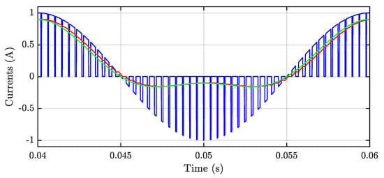
Figure 4.
Input current: instantaneous value (blue), its averaged value over the switching period (red), and calculated value (green) in case of single-phase unbalance for m = 0.4, I = Ia = 1 A and φ = 0°.
4. Evaluation of Capacitors and DC-Link Voltage Ripples
Likewise, Equation (5), the instantaneous capacitors’ voltages v1 and v2 and the total dc-link voltage v, can be defined in terms of low- and high-frequency harmonic components as
where V1 and V2 are the dc (average) voltage components of upper and lower capacitors, respectively; V is the average voltage of the total dc-link, and are the low-frequency parts of the of upper and lower capacitors, respectively; is the low-frequency component of the total dc-link voltage; and are the high-frequency (switching) components of upper and lower capacitors, respectively and, finally, is the high-frequency (switching) component of the total dc-link voltage.
Since the upper and lower capacitors have identical values Cdc, the dc component V is simply determined by the supply voltage Vdc and the voltage drop across the resistor Rdc
By assuming that the capacitive reactance dominates the equivalent dc-link RL impedance at switching frequency fsw, the whole switching current ripple circulates through the dc-link capacitor. In this case, the equivalent dc-link capacitor is Cdc/2, and the total dc-link voltage ripple can be calculated as
4.1. Peak-To-Peak Voltage Ripple
The instantaneous, peak-to-peak, dc-link voltage ripple can be computed by replacing Equation (5) into Equation (14) and integrating over any abstract period t, leading to
In the following equations, the index “pk” denotes the “peak” value, whereas “pp” denotes the “peak-to-peak” value.
The peak-to-peak “pp”, dc-link voltage ripple as a function of modulation index and phase angle, over a switching period Tsw can be defined as
Determining the peak-to-peak dc-link voltage ripple, both balanced and unbalanced loads are considered. With reference to Figure 5 and in case of balanced output currents, the time intervals are given by:
where the application time intervals ta, tb, and tc are expressed by the set of equations
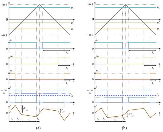
Figure 5.
Input current and dc-link voltage ripple in one switching period in case of balanced loads: (a) ia ≥ Idc, (b) ia < Idc.
4.1.1. Balanced Load
Thanks to the inverter input current periodicity i(t), the evaluation of the dc-link voltage ripple can be reduced to the phase angle range 0 ≤ ϑ ≤ π/3. In this interval and, depending on the value of Idc, two different cases can be distinguished according to Figure 5: ia ≥ Idc (Figure 5a) and ia < Idc (Figure 5b).
The actual peak dc-link voltage ripple can be obtained by merging the results corresponding to these two cases. Concerning Figure 5, the peaks “pk” of the total dc-link voltage ripples are expressed as
where and are called “first” and “second” envelopes of total dc-link voltage ripple, respectively, according to Figure 5a (ia ≥ Idc). has been labeled as “third” envelope according to Figure 5b in the case of ia < Idc.
By introducing Equations (9) and (17) into Equation (19), the peak in dc-link voltage ripple in the case of a system with unity power factor becomes
Equation (20) can be normalized by I/(fsw Cdc), leading to the normalized set of ripple functions
The peak in the dc-link voltage ripple is determined from Equation (21) as
As an example, the normalized voltage ripples for both capacitors, as well as for the total dc-link, are shown in Figure 6. To obtain the depicted simulation results, the following initial parameters were assumed, specifically fsw = 2.4 kHz and load with unity power factor. Subfigures labeled as “(a)” are plotted for m = 0.4 and those with “(b)” for m = 0.5.
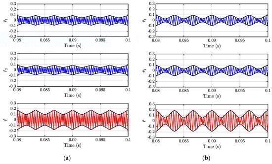
Figure 6.
Normalized capacitors switching voltage ripple ( and ) (blue traces), dc-link switching voltage ripple () (red trace) and calculated envelopes (black traces) over a fundamental period for m = 0.4 (a) and m = 0.5 (b) in case of φ = 0° and balanced load.
Since the positive and negative envelopes of normalized voltage ripple, depicted in Figure 6, are symmetric along the zero value, to calculate the peak-to-peak value of those quantities, one could simply multiply Equation (22) by 2, eventually obtaining the distribution of the normalized peak-to-peak dc-link voltage ripple. Figure 7 depicts its profile for the phase range ϑ = [0, π/3].
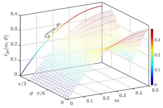
Figure 7.
Normalized peak-to-peak dc-link switching voltage ripple () as a function of the modulation index (m) and the phase angle (ϑ) over the period [0, π/3] and at φ = 0°. Maximum normalized peak-to-peak dc-link switching voltage ripple () as a function of the modulation index (m) in the left-hand plane.
Based on Figure 7 and Equation (22), the maximum peak–peak voltage ripple can be analytically determined by setting ϑ equal to 0 (with periodicity of π/3) as
4.1.2. Unbalanced Load—Two-Phase Load (Phases a and b)
Figure 8 shows profiles of the instantaneous input dc current and capacitor voltage ripple in one switching period, operating with an unbalanced load. The latter was emulated by setting one phase current to zero (in this case, the phase current c is zero), while the remaining phases works normally.
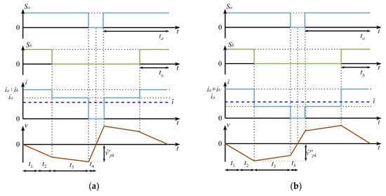
Figure 8.
Input current and voltage ripple in one switching period in case of an unbalanced load (only two phases). (a) ia ≥ ī (b) ia < ī.
According to Figure 8, and considering application intervals t4 and t3 + t4, the peaks in the dc-link voltage ripple can be mathematically described based on Equation (15) as
By introducing Equations (10) and (17) into Equation (24) and eventually normalizing by I/(fswCdc), the normalized peaks of the total dc-link voltage ripple in case of Ia = Ib and zero phase angle become
It should be noted that Equation (25) is valid within the phase angle range [4π/3, 7π/3] and ic = 0, as depicted in Figure 8. Similar expressions can be derived for other combinations of the phases. The normalized voltage ripple for both capacitors, as well as for the total dc-link, are shown in Figure 9. The initial parameters considered in the simulations are fsw = 2.4 kHz and load with unity power factor. Subfigures labeled as “(a)” are plotted for m = 0.4 and those with “(b)” for m = 0.5.
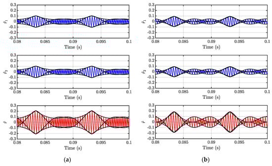
Figure 9.
Normalized capacitors switching voltage ripple ( and ) (blue traces), dc-link switching voltage ripple () (red trace) and calculated envelopes (black traces) over a fundamental period for m = 0.4 (a) and m = 0.5 (b) in case of φ = 0° and unbalanced load (two-phase load).
The normalized peak-to-peak dc-link voltage ripple calculated by Equation (25) is shown in Figure 10 within the phase range ϑ = [4π/3, 7π/3].
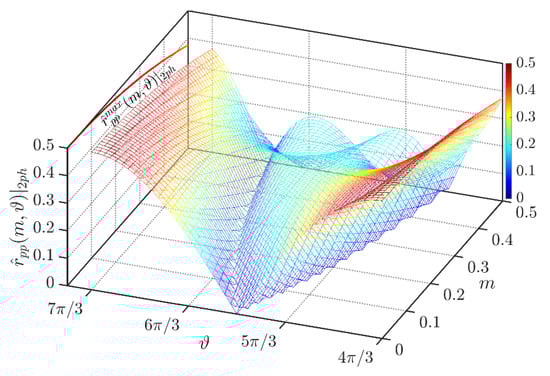
Figure 10.
Normalized peak-to-peak dc-link switching voltage ripple () as a function of the modulation index (m) and the phase angle (ϑ) over the period [4π/3, 7π/3] in case of φ = 0°. Maximum normalized peak-to-peak dc-link switching voltage ripple () as a function of the modulation index (m) in the left-hand plane.
Based on the profile of the ripple in Figure 10, the normalized maximum peak-to-peak dc-link voltage ripple in case of I = Ia = Ib can be analytically determined by setting in Equation (25) ϑ equal to 4π/3 (or 7π/3), leading to
4.1.3. Unbalanced Load—Single-Phase Load (Only Phase a)
The input dc current and dc-link voltage ripple, within one switching period, in the case of a single-phase unbalanced load, are depicted in Figure 11.
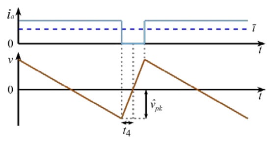
Figure 11.
Input current and voltage ripple in one switching period in case of a single-phase unbalanced load (only phase a).
In this section, a single-phase unbalance is considered: two phases are disconnected, and the three-phase inverter supplies the power via the only remaining phase. In this context, and according to Figure 11, the peak in the dc-link voltage ripple can be computed based on Equation (15) as
Replacing Equations (11) and (17) into Equation (27) and normalizing by I/(fswCdc), the normalized dc-link voltage ripple (peak) at unity power factor is
For validating analytical developments, the normalized ripple voltage for both capacitors and the total dc-link are depicted in Figure 12 for two modulation indices m = 0.4 and m = 0.5 in the case of fsw = 2.4 kHz and unity power factor. As can be seen, the envelopes wrap up the instantaneous ripples perfectly.
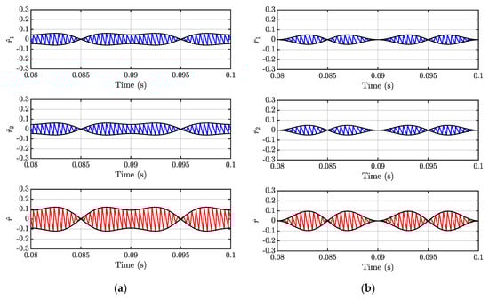
Figure 12.
Normalized capacitors switching voltage ripple ( and ) (blue traces), dc-link switching voltage ripple () (red trace) and calculated envelopes (black traces) over a fundamental period for m = 0.4 (a) and m = 0.5 (b) in case of φ = 0° and unbalanced load (single-phase load).
Figure 13 depicts the normalized peak-to-peak dc-link voltage ripple amplitude in the phase range ϑ = [−π/2, π/2].
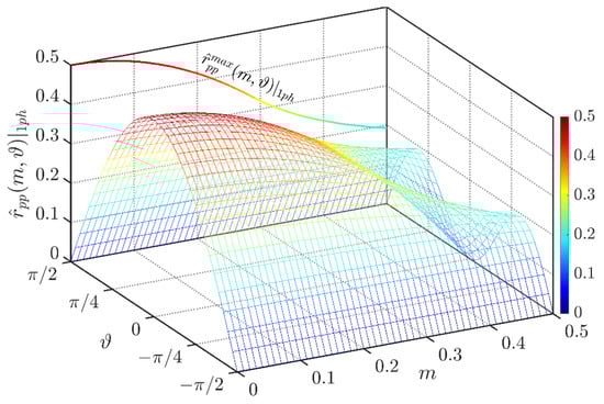
Figure 13.
Normalized peak-to-peak dc-link switching voltage ripple () as a function of the modulation index (m) and the phase angle (ϑ) over the period [−π/2, π/2] and φ = 0°. Maximum normalized peak-to-peak dc-link switching voltage ripple () as a function of the modulation index (m) in the left-hand plane.
In this occasion, the maximum of the normalized peak-to-peak dc-link voltage ripple has been determined numerically (colored trace on the 2D plane of the 3D plot in Figure 13), due to the fact that at higher modulation indices m > 0.3 there is no unique phase angle that corresponds to the maximum ripple function.
4.2. Rms of the Total dc-Link Voltage Ripple
As is visible in Figure 5, Figure 8 and Figure 11, the switching ripple profile does not always present a triangular-like waveform. Therefore, only knowing the ripple envelopes is not enough for the rms calculation.
Noticing that the voltage ripple waveform can be considered as a linear piecewise function, the rms can be computed by studying each interval k by itself. Each k-th portion is the composition of dc (offset) and ac (sawtooth-like profile) components over each time interval. Thanks to the orthogonality of their spectra, it is possible to compute the rms value in each interval, composing the rms of the two components as
Subsequently, the rms within each switching period can be calculated, employing results available from Equation (29) as
Finally, the actual rms voltage ripple is obtained as
This approach has been used in the following subsections.
4.2.1. Balanced Loads
Considering the voltage profiles visible in Figure 5, and its timing in Equation (17), it is possible to compute the rms in case of balanced load in both cases ia ≥ Idc and ia < Idc. Knowing that √3 is the sawtooth crest factor, Equation (29) can be explicitly rewritten as
For the odd symmetry of the voltage ripple, the rms over the whole switching period Tsw can be calculated by composing the individual rms over the four k intervals of Equation (32) as
Finally, taking advantage of the voltage ripple symmetry (in balanced case only) and assuming unity power factor, the rms of the total dc-link voltage ripple is obtained as
The analysis is limited to one-sixth of the fundamental period (T/6) thanks to the resulting symmetry of the input current, as shown in Figure 2. Consequently, the voltage ripple is symmetrical as well and the domain of integration is reduced from [0, 2π] to [0, π/3]. Equation (34) can be normalized as
Equation (35) is has been depicted in Figure 14 under the label “3ph”.
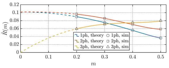
Figure 14.
Normalized dc-link switching voltage ripple rms () as a function of the modulation index (m) for studied cases: balanced load (3ph), two-phase load (2ph), and single-phase load (1ph).
4.2.2. Unbalanced Loads—Only Two Phases (Phases a and b)
Considering the voltage profile visible in Figure 8 and taking advantage of the pulse timings of Equation (17) rewritten as
it is possible to compute the rms in both cases, ia ≥ ī, and ia < ī. Knowing that √3 is the sawtooth crest factor, Equation (29) can be explicitly rewritten as
For the odd symmetry of the voltage ripple, the rms over the whole switching period Tsw can be calculated by composing the individual rms over the three k intervals of Equations (37) as
Finally, integrating over the phase range ϑ = [4π/3, 7π/3]
Equation (39) can be normalized as
Equation (40) is depicted in Figure 14 under the label “2ph”.
4.2.3. Unbalanced Loads—A Single-Phase Load (Only Phase a)
As shown in Figure 11, the voltage ripple profile is much simpler compared to the one that is visible in Figure 5. Taking advantage of the triangle like waveform, the rms in the whole switching period can be straightforwardly calculated, without considering time slots, as
Finally, taking advantage of the voltage ripple symmetry, the rms voltage ripple is obtained as
Equation (42) can be normalized as
Equation (43) is depicted in Figure 14 under the label “1ph”.
It should be mentioned that by replacing Cdc/2 with Cdc, one can obtain the capacitor voltage ripple rms rather than only the rms of the total dc-link voltage.
As is visible in Figure 14, “1ph” voltage ripple rms outperforms both the “2ph” and the “3ph” voltage ripple rms in case of m ≥ 0.3. For low values of m, “3ph” presents the best rms performance. Conversely, for high values of m, “3ph” shows the worst performance among the studied three cases.
5. Experimental Results
To validate the analytical developments, some experimental tests on a three-phase, four-wire, split capacitor inverter (shown in Figure 1) were performed. As discussed before, an RLC load able to simulate a unity power factor grid connection was employed. An insulated gate bipolar transistor (IGBT) three-phase module constitutes the experimental setup of Figure 15a (PS22A76, 1200V, 25A, Mitsubishi Electric Corporation, Tokyo, Japan) connected to a split capacitor dc-link made out of two film capacitors connected via decoupling inductance to a dc voltage supply (GEN100-33, 100V, 33A, TDK-Lambda Corporation, Tokyo, Japan). On the ac side, an induction machine (2.2 kW [26]) represents the RL series circuit. Meanwhile, the RC parallel circuit is obtained by the parallel connection of ac capacitors and a resistor for each phase (Figure 15b). Sensing of the ac phase currents, the ac phase voltages, and the dc bus voltage were done with help of current sensors (LA 55-P, 55A, LEM Europe GmbH, Fribourg, Switzerland), isolated voltage probes (PICO TS057, Tyler, TX, USA), and digital oscilloscope (DS1054Z, Rigol, Beijing, China) respectively. Employing decoupling optical fibers, a digital signal processor (DSP) board (TMS320F28379D, Texas Instruments, Dallas, TX, USA) drives the voltage source inverter. Data were acquired using three digital oscilloscopes (sampling frequency 5 MHz, without pre-filtering) and later plotted via MATLAB platform (MathWorks, Natick, MA, USA). All the circuital parameters are summarized in Table 1.
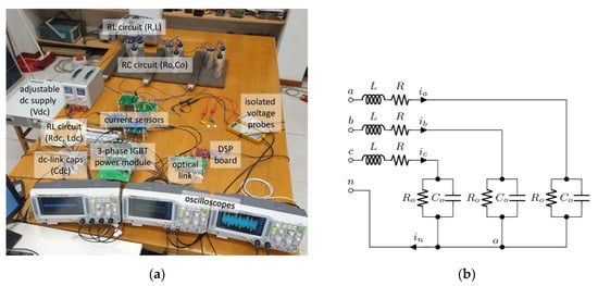
Figure 15.
(a) Experimental laboratory test bench; (b) Unity power factor load.

Table 1.
Experimental setup parameters.
Since this paper refers to the switching voltage ripple, it is important to deal with an ac output current that is as clean as possible from the corresponding ac current ripple. To minimize this current ripple, an induction motor was chosen as a load for its high inherent inductive component. However, as shown in [26] and reported in Table 1, inductance at the switching frequency is lower in comparison to its corresponding value at the fundamental frequency. Since, in this paper, the main focus is drawn to the grid-connected applications, only high values of the modulating index range were tested (m ≥ 0.2). In this section, only the total dc-link voltage Vdc in a balanced modulation scheme is presented.
Moreover, as is visible in Figure 15b and from the parameters of Table 1, a load with unity power factor has been employed. This choice introduces direct proportionality between the amplitude of the ac current I and the modulation index m, according to
where Zeq is the unity power factor load impedance with reference to Table 1, Zeq ≅ 18.8 Ω.
In Figure 16, the dc-link voltage ripple was depicted. It can be seen that, in both cases (m = 0.4 and m = 0.5), the experimental results reasonably match the analytical envelopes calculated by Equation (21), taking into account the scaling factor of the load discussed in Equation (44). The residual ac current ripple causes a small degradation of the voltage ripple profile, noticeable in the upper part of the voltage displayed in Figure 16.
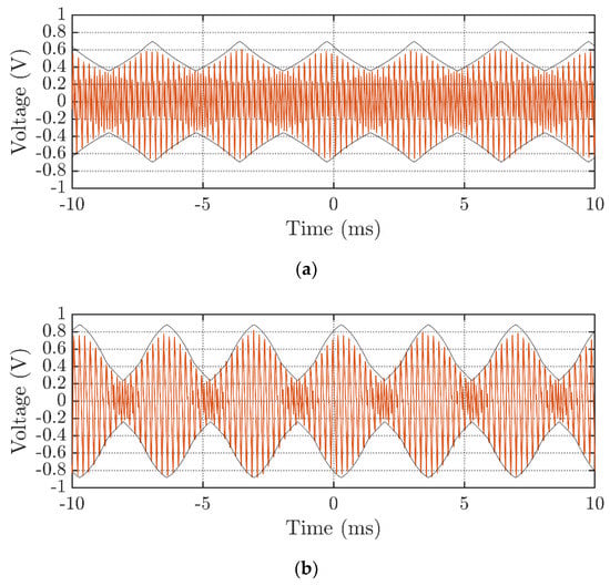
Figure 16.
Dc link voltage switching ripple at: (a) m = 0.4; (b) m = 0.5.
A good correlation between the experimental voltage ripple profile and the envelopes (analytically derived) is validated by the voltage ripple rms measurement presented in Figure 17. It can be readily seen that the voltage ripple rms in the case of three balanced currents (3ph) of Figure 14 strongly differ from the one visible in Figure 17. This difference is due to the different testing conditions, as discussed above. Updating the rms function of Equation (34) by taking into consideration Equation (44), one could obtain the following.
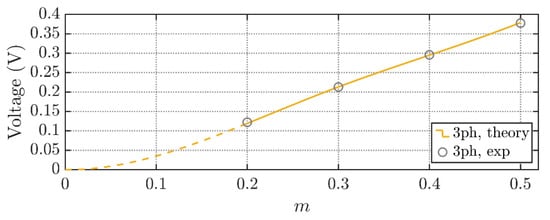
Figure 17.
Dc link voltage switching ripple rms for high values of modulation index.
The latter expression is depicted in Figure 17. The test points perfectly follow the analytical profile given by Equation (45).
For the sake of completeness, the output current and voltage are depicted in Figure 18. As visible in Figure 18a, a set of balanced sinusoidal phase currents was obtained with a small residual current ripple. To verify the harmonic content of the phase currents, Figure 18b is depicted. As can be noted, the harmonic at switching frequency stays within 3% of the fundamental current phase component and the total THD of a phase current is 4.16%. On the other hand, Figure 18c shows the two-level phase voltage typical for this kind of converter, along with its fundamental component at 50 Hz and the corresponding phase current. The latter plot confirms operating conditions at unity power factor.
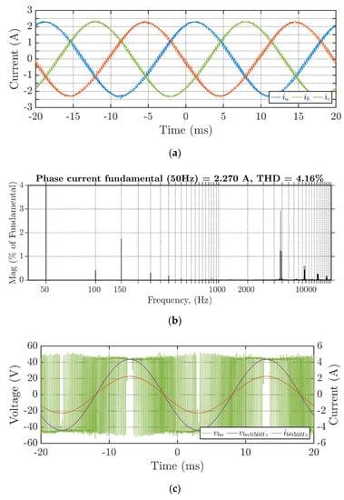
Figure 18.
(a) Balanced phase currents (@ m = 0.5); (b) Harmonic spectrum of a phase current (phase b, @ m = 0.5); (c) Phase output voltage (phase b) and its fundamental component in comparison with phase current (@ m = 0.5).
The overall experimental results validate the analytical findings and reasonably match with the numerical results, ensuring the accuracy of the proposed analysis.
6. Conclusions
This paper deals with the analysis of input current and voltage ripple in three-phase, four-wire, split-capacitor PWM inverters. Reference is made to the sinusoidal PWM modulation and sinusoidal three-phase load currents with an almost unity power factor, representing a typical grid-connected application. Firstly, the input current and voltage ripple components were analytically determined for both the capacitors’ and total dc-link. Secondly, analytical formulations of the peak-to-peak values of the voltage ripples were determined in the case of balanced three-phase and unbalanced (two-phase and single-phase) output ac currents. These three study cases were selected as extreme operating conditions, while the other, intermediate modes can be easily derived from the presented cases. Finally, the rms functions of the voltage ripple were calculated in the aforementioned cases for both capacitor voltage and total dc-link voltage. It is worth mentioning that the obtained results can help in designing the whole ac/dc conversion system and sizing the dc-link capacitors. Numerical simulations were carried out to prove the effectiveness of the analytical developments for peak-to-peak and rms. A balanced three-phase load was considered to experimentally verify all findings by a laboratory prototype.
Author Contributions
Conceptualization, M.H., R.M., A.V., M.R., and G.G.; methodology, M.H., R.M., A.V., M.R., and G.G.; software, M.H., A.V., and R.M.; validation, M.H., R.M., and A.V.; formal analysis, M.H., R.M., A.V., and G.G.; investigation, M.H., A.V., and R.M.; resources, M.H., A.V., and R.M.; data curation, M.H., A.V., and R.M.; writing—original draft preparation, M.H., A.V., and R.M.; writing—review and editing, M.H., R.M., A.V., M.R., and G.G.; visualization, M.H., A.V., and R.M.; supervision, M.R. and G.G. All authors have read and agreed to the published version of the manuscript.
Funding
This research received no external funding.
Conflicts of Interest
The authors declare no conflict of interest.
References
- Nascimento, C.F.; Diene, O.; Watanabe, E.H. Analytical Model of Three-Phase Four-Wire VSC Operating as Grid Forming Power Converter under Unbalanced Load Conditions. In Proceedings of the 2017 IEEE 12th International Conference on Power Electronics and Drive Systems (PEDS), Honolulu, HI, USA, 12–15 December 2017; pp. 1219–1224. [Google Scholar]
- Li, A.; Jiang, D.; Kong, W.; Qu, R. Four-Leg Converter for Reluctance Machine With DC-Biased Sinusoidal Winding Current. IEEE Trans. Power Electron. 2019, 34, 4569–4580. [Google Scholar] [CrossRef]
- Ghosh, R.; Narayanan, G. Control of Three-Phase, Four-Wire PWM Rectifier. IEEE Trans. Power Electron. 2008, 23, 96–106. [Google Scholar] [CrossRef]
- Aredes, M.; Hafner, J.; Heumann, K. Three-Phase Four-Wire Shunt Active Filter Control Strategies. IEEE Trans. Power Electron. 1997, 12, 311–318. [Google Scholar] [CrossRef]
- Viatkin, A.; Hammami, M.; Grandi, G.; Ricco, M. Analysis of a Three-Phase Four-Leg Front-End Converter for EV Chargers with Balanced and Unbalanced Grid Currents. In Proceedings of the IECON 2019—45th Annual Conference of the IEEE Industrial Electronics Society, Lisbon, Portugal, 14–17 October 2019; pp. 3442–3449. [Google Scholar]
- Hintz, A.; Prasanna, R.; Rajashekara, K. Comparative Study of Three-phase Grid Connected Inverter Sharing Unbalanced Three-phase and/or Single-phase systems. In Proceedings of the 2015 IEEE Energy Conversion Congress and Exposition (ECCE), Montreal, QC, Canada, 20–24 September 2015; pp. 6491–6496. [Google Scholar]
- Kim, J.-H.; Sul, S.-K. A Carrier-Based PWM Method for Three-Phase Four-Leg Voltage Source Converters. IEEE Trans. Power Electron. 2004, 19, 66–75. [Google Scholar] [CrossRef]
- Viatkin, A.; Mandrioli, R.; Hammami, M.; Ricco, M.; Grandi, G. Theoretical Analysis of the AC Current Ripple in Three-Phase Four-Leg Sinusoidal PWM Inverters. In Proceedings of the 2020 IEEE 29th International Symposium on Industrial Electronics (ISIE), Delft, The Netherlands, 17–19 June 2020; pp. 796–801. [Google Scholar]
- Mandrioli, R.; Viatkin, A.; Hammami, M.; Ricco, M.; Grandi, G. A Comprehensive AC Current Ripple Analysis and Performance Enhancement via Discontinuous PWM in Three-Phase Four-Leg Grid-Connected Inverters. Energies 2020, 13, 4352. [Google Scholar] [CrossRef]
- Zhao, W.; Ruan, X.; Yang, D.; Chen, X.; Jia, L. Neutral Point Voltage Ripple Suppression for a Three-Phase Four-Wire Inverter With an Independently Controlled Neutral Module. IEEE Trans. Ind. Electron. 2017, 64, 2608–2619. [Google Scholar] [CrossRef]
- Lin, Z.; Ruan, X.; Jia, L.; Zhao, W.; Liu, H.; Rao, P. Optimized Design of the Neutral Inductor and Filter Inductors in Three-Phase Four-Wire Inverter With Split DC-Link Capacitors. IEEE Trans. Power Electron. 2019, 34, 247–262. [Google Scholar] [CrossRef]
- Grandi, G.; Loncarski, J. Evaluation of current ripple amplitude in three-phase PWM voltage source inverters. In Proceedings of the 2013 International Conference-Workshop Compatibility in Power Electronics, Ljubljana, Slovenia, 5–7 June 2013; pp. 156–161. [Google Scholar]
- Vujacic, M.; Hammami, M.; Srndovic, M.; Grandi, G. Theoretical and experimental investigation of switching ripple in the DC-link voltage of single-phase H-bridge PWM inverters. Energies 2017, 10, 1189. [Google Scholar] [CrossRef]
- Chen, T.; Li, S.; Fahimi, B. Analysis of DC-Link Voltage Ripple in Voltage Source Inverters without Electrolytic Capacitor. In Proceedings of the IECON 2018—44th Annual Conference of the IEEE Industrial Electronics Society, Washington, DC, USA, 21–23 October 2018; pp. 1041–1048. [Google Scholar]
- Chowdhury, S.; Gurpinar, E.; Ozpineci, B. High-Energy Density Capacitors for Electric Vehicle Traction Inverters. In Proceedings of the 2020 IEEE Transportation Electrification Conference & Expo (ITEC), Chicago, IL, USA, 23–26 June 2020; pp. 644–650. [Google Scholar]
- Lee, J.-H.; Lee, K.-B. Optimal phase shifted method to reduce current ripples for parallel grid-connected voltage source inverter under unequal DC-link voltages. In Proceedings of the 2017 IEEE Energy Conversion Congress and Exposition (ECCE), Cincinnati, OH, USA, 1–5 October 2017; pp. 4589–4594. [Google Scholar]
- Hammami, M.; Vujacic, M.; Grandi, G. Dc-link current and voltage ripple harmonics in three-phase three-level flying capacitor inverters with sinusoidal carrier-based PWM. In Proceedings of the 2018 IEEE International Conference on Industrial Technology (ICIT), Lyon, France, 20–22 February 2018; pp. 664–669. [Google Scholar]
- Kai, L.; Mengshu, L.; Zhengfeng, L.; Zhenghua, D.; Shaoju, T. Analytical closed-form expressions of DC current ripple for three-level neutral point clamped inverters with space-vector pulse-width modulation. IET Power Electron. 2016, 9, 930–937. [Google Scholar] [CrossRef]
- Gopalakrishnan, K.S.; Das, S. Analytical Expression for RMS DC Link Capacitor Current in a Three-Level Inverter. In Proceedings of the Centenary Conference Electrical Engineering, Indian Institute of Science, Bangalore, India, 15–17 December 2011; pp. 1–6. [Google Scholar]
- Vujacic, M.; Hammami, M.; Srndovic, M.; Grandi, G. Analysis of dc-link voltage switching ripple in three-phase PWM inverters. Energies 2018, 11, 471. [Google Scholar] [CrossRef]
- Escobar, G.; Valdez, A.A.; Torres-Olguin, R.E.; Martinez-Montejano, M.F. A Model-Based Controller for A Three-Phase Four-Wire Shunt Active Filter With Compensation of the Neutral Line Current. IEEE Trans. Power Electron. 2007, 22, 2261–2270. [Google Scholar] [CrossRef]
- Fabricio, E.L.L.; Junior, S.C.S.; Jacobina, C.B.; de Rossiter Correa, M.B. Analysis of Main Topologies of Shunt Active Power Filters Applied to Four-Wire Systems. IEEE Trans. Power Electron. 2018, 33, 2100–2112. [Google Scholar] [CrossRef]
- Khadkikar, V.; Chandra, A.; Singh, B. Digital signal processor implementation and performance evaluation of split capacitor, four-leg and three H-bridge-based three-phase four-wire shunt active filters. IET Power Electron. 2011, 4, 463–470. [Google Scholar] [CrossRef]
- Fraser, M.E.; Manning, C.D.; Wells, B.M. Transformerless four-wire PWM rectifier and its application in AC-DC-AC converters. IEE Proc.-Electr. Power Appl. 1995, 142, 410–416. [Google Scholar] [CrossRef]
- Tayebi, S.M.; Batarseh, I. Mitigation of Current Distortion in a Three-Phase Microinverter With Phase Skipping Using a Synchronous Sampling DC-Link Voltage Control. IEEE Trans. Ind. Electron. 2018, 65, 3910–3920. [Google Scholar] [CrossRef]
- Grandi, G.; Loncarski, J.; Srndovic, M. Analysis and minimization of output current ripple for discontinuous pulse-width modulation techniques in three-phase inverters. Energies 2016, 9, 380. [Google Scholar] [CrossRef]
© 2020 by the authors. Licensee MDPI, Basel, Switzerland. This article is an open access article distributed under the terms and conditions of the Creative Commons Attribution (CC BY) license (http://creativecommons.org/licenses/by/4.0/).