Abstract
The development and the validation of an averaged-value mathematical model of an asymmetrical hybrid multi-level rectifier is presented in this work. Such a rectifier is composed of a three-level T-type unidirectional rectifier and of a two-level inverter connected to an open-end winding electrical machine. The T-type rectifier, which supplies the load, operates at quite a low switching frequency in order to minimize inverter power losses. The two-level inverter is instead driven by a standard sinusoidal pulse width modulation (SPWM) technique to suitably shape the input current. The two-level inverter also plays a key role in actively balancing the voltage across the DC bus capacitors of the T-type rectifier, making unnecessary additional circuits. Such an asymmetrical structure achieves a higher efficiency compared to conventional PWM multilevel rectifiers, even considering extra power losses due to the auxiliary inverter. In spite of its advantageous features, the asymmetrical hybrid multi-level rectifier topology is a quite complex system, which requires suitable mathematical tools for control and optimization purposes. This paper intends to be a step in this direction by deriving an averaged-value mathematical model of the whole system, which is validated through comparison with other modeling approaches and experimental results. The paper is mainly focused on applications in the field of electrical power generation; however, the converter structure can be also exploited in a variety of grid-connected applications by replacing the generator with a transformer featuring an open-end secondary winding arrangement.
1. Introduction
Multi-level converters have proved in the last decades to be a viable alternative to conventional topologies in medium-voltage, high-power, industrial applications, but today, their field of applications is rapidly spreading toward low-power and low-voltage ranges. Main advantages of multi-level converters are basically those of an improved harmonic content of AC voltages and currents and of a reduction of power switch voltage ratings [1,2], the main drawback being a greater complexity. Open-winding (OW) configurations, consisting of an AC machine fed by two power converters [3,4,5,6], can be deemed as a special kind of multi-level converter [7]. Different configurations, control schemes, and modulation techniques dealing with OW systems have been discussed in the literature [8,9,10]. Some OW configurations embedding multi-level converters have also been recently developed [11,12,13]. Among them, a high efficiency asymmetrical hybrid multilevel inverter for motor drives has been presented and analyzed in [12] featuring a particular asymmetrical structure where two different kinds of converters are connected at the two sides of an OW AC machine with different functions. Specifically, a main multilevel converter supplies the load, and an auxiliary two-level inverter acts as an active power filter. Such an approach has also been used in [13] to realize an asymmetrical hybrid unidirectional T-type rectifier (AHUTR) for gen-set applications, tailored around an open-end winding permanent magnet synchronous generator (PMSG), as shown in Figure 1. According to the AHUTR topology, the open-end winding PMSG on one side supplies the electrical load through the main converter, a T-type rectifier (TTR), also commonly known as a Vienna rectifier, and on the other side, it is connected to an auxiliary two-level inverter (TLI). The main converter processes the whole power delivered to the load, and thus, it is operated at the fundamental frequency in order to minimize the switching power losses. The TLI is instead driven by a high switching frequency PWM technique to suitably shape the phase currents. Therefore, a stable output DC voltage and almost sinusoidal input currents are obtained, achieving a higher efficiency than comparable conventional PWM rectifiers [12]. The AHUTR structure is also of general applicability, being exploitable in grid-connected applications by replacing the generator with a transformer featuring an open-end secondary winding, as shown in Figure 1, but it is more complex than conventional rectifiers, requiring suitable mathematical tools for control and optimization purposes. The aim of this work is thus to provide an essential tool for the design of the control system of an AHUTR by developing an averaged-value model (AVM) of the system. In general, averaged-value techniques approximate the model of a switching converter to a continuous system by considering the values taken by the variables along a switching period as constant. They are useful when designing and testing control algorithms, as well as to develop efficiency optimization techniques, because a high frequency dynamic analysis is not required, differently than power circuits and filters design. Specifically, an AHUTR AVM has been developed with the aim to support the design of effective solutions to maximize system efficiency, to provide a stable DC output voltage, to cancel low-order undesired harmonics from the phase currents, to equalize the Vienna rectifier DC bus capacitor voltages, and to control the TLI DC bus voltage. Furthermore, the developed model is valuable in tuning voltage and current regulators.
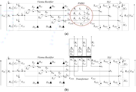
Figure 1.
AHUTR for electrical power generation (a) and grid-connected (b) applications.
2. Asymmetrical Hybrid Unidirectional T-Type Rectifier
According to Figure 1, an AHUTR supplies the load through a Vienna rectifier switching at fundamental frequency. In electricity generation applications, this rectifier is connected to one end of an open winding electrical generator, very often a PMSG. For grid-connected applications, the electrical generator is replaced by a transformer with an open-end secondary winding. While remarkably reducing the switching power losses, low switching frequency operations would, however, produce highly distorted phase currents. This is prevented by an active power filter based on a conventional TLI, which is connected to the other end of the electrical machine winding. Such an inverter features a lower DC bus voltage compared to the Vienna rectifier and exploits a floating capacitor to reduce the complexity of the system and to prevent the occurrence of zero sequence currents [11,12,13]. The efficiency of the Vienna rectifier can be increased by using low on-state voltage drop power devices, thus optimizing the design of this converter for low conduction power losses. On the other hand, the design of the TLI can be optimized for high switching frequency operation, by using fast power devices with lower voltage ratings. A key feature of the AHUTR topology is that the voltages of the two Vienna rectifier DC bus capacitors can be independently regulated through the TLI, thus making unnecessary additional power converters or special PWM strategies.
In the AHUTR topology, three bidirectional switches Sij, (i = a, b, c and j = 1, 2) are connected between the midpoint n′ of the Vienna rectifier and the rectifier poles [14]. The generic i-phase voltage ViTTR between the rectifier input terminal iM and the mid-point n″ of the Vienna rectifier DC bus is given by
where VDC′ is the DC bus voltage. Hence, three different levels can be taken by the Vienna rectifier input voltage, namely: −VDC′/2, VDC′/2, and 0, according to the rectifier i-pole state li′.
On the TLI side, the voltage between the TLI i-phase output terminal iT and the mid-point n′ of the TLI DC bus is given by:
providing two voltage levels, namely, −VDC″/2 and VDC″/2, according to the inverter i-pole state li″.
The voltage across a phase winding is given by
where VDC′ and VDC″ are the DC bus voltages of the Vienna rectifier and the TLI, respectively, and Vn′n″ is the voltage between the mid points n′ and n″ of the two DC buses, which can be expressed as
According to (2) and (3), the OW structure of Figure 1, featuring twelve power switches, is equivalent to a six-level neutral point clamped (NPC) or flying capacitor (FC) converter, which would, however, encompass thirty power switches [12]. As shown in Figure 2, the AHUTR requires a complex control system to suitably coordinate the operations of the two converters in order to regulate the DC output voltage, to cancel low-order harmonics from phase currents, to equalize the Vienna rectifier DC bus capacitor voltages, and to control the TLI DC bus voltage [14,15].
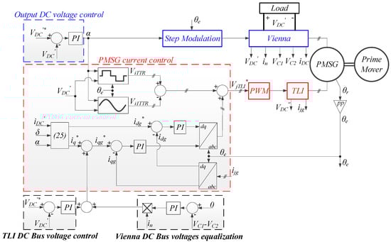
Figure 2.
Block diagram of the control system of the AHUTR for electrical power generation applications.
3. Averaged-value Model of the System
The averaged-value mathematical model of the system includes three sub-models: of the electrical machine, of the Vienna rectifier, and of the TLI.
3.1. Open-Winding PMSG Model
It is assumed that the stator windings produce sinusoidal magnetomotive forces; moreover, effects of the saturation of the magnetic core are neglected. Under these assumptions, the surface-mounted PMSG model in an orthogonal qd reference frame synchronous to the rotor flux is given by the following sets of Equations:
where iqs, ids, Vqs, Vds, λqs, and λds are the components of stator current, voltage, and flux in the qd axis; Ls is the stator inductance; λpm is the linkage flux of permanent magnets; Te is the electromagnetic torque; J is the total mechanical inertia; F is the rotor friction; ωre = ppωr is the rotor speed; and pp is the amount of pole pairs. The rotational terms ωreλds and ωreλqs account for the qd axis back-emf Eq and Ed, respectively.
The averaged-value PMSG phase voltage Vig is obtained as the difference between the fundamental harmonic of the Vienna rectifier input voltage and the fundamental harmonic of the TLI output voltage. The voltage Vn′n″ between the mid points of the two DC buses can be neglected for averaged-value analysis, since it only includes high frequency harmonics [13].
PMSG phase voltages can be expressed in a qd synchronous reference frame to the back-EMF vector as a function of qd components of voltages and by:
A block scheme of the PMSG model is shown in Figure 3.
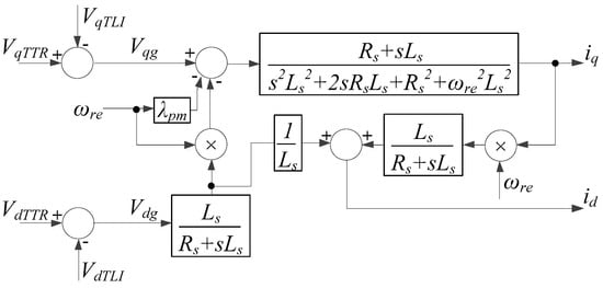
Figure 3.
Block scheme of the permanent magnet synchronous generator (PMSG) model.
Similarly, a three-phase open secondary winding transformer (OSWT) can be modeled in an orthogonal qd reference frame synchronous to the primary voltage vector according to:
where iq1, id1, iq2, and id2 are the q- and d-axis components of the primary and secondary winding currents, while Vq1, Vd1, Vq2, Vd2 and λq1, λd1, λq2, λd2, are the q- and d-axis components of the primary and secondary winding voltages and fluxes. Ls1 and Ls2 are the self-inductances and Lm is the magnetization inductance. The angular frequency of the grid voltage is indicated as ωe. The secondary windings are connected to the TTR and TLI, and thus, the phase winding voltages are given by:
3.2. Vienna Rectifier Model
The Vienna rectifier switches at the fundamental frequency, according to Table 1, where θe is the angular displacement of the fundamental harmonic of the winding phase voltage and α is the switching angle of Sij, (i = a, b, c and j = 1, 2).

Table 1.
Vienna rectifier switching table.
Assuming the output voltage VDC′ is constant, actual values of Vienna rectifier input phase voltages ViTTR are thus given by:
To avoid improper operations leading to extra power losses and voltage distortion, the angular displacement φTTR between the fundamental harmonics of voltage ViTTR and current must be set lower than . Dealing with an electrical power generation application, a vector diagram of AC variables is shown in Figure 4a, where φ is the phase displacement between the PMSG back-EMF and the current . δ represents the angle between the voltage and the q axis, and is set to allow a reactive power flow between the Vienna rectifier and PMSG, associated to the inductive elements of the electrical machine.
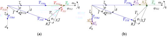
Figure 4.
Vector diagram of AC variables: (a) considering VTLI, (b) neglecting VTLI.
Neglecting, for simplicity, the voltage VTLI generated by the auxiliary inverter, which is an independent variable and whose amplitude is significantly lower than Vi1TTR, the amplitude of the fundamental harmonic of the TTR input voltage Vi1TTR is obtained as a function of the switching angle α and DC bus voltage VDC′ as follows:
where mTTR is the modulation index of the Vienna rectifier. According to the vector diagram of Figure 4b, qd components of the voltage can be written as:
while the active and reactive powers are given by:
where PTTR and QTTR are the active and reactive power, respectively, processed by the Vienna rectifier, PR and QX are the active power wasted in the stator resistance R and the reactive power due to the PMSG synchronous reactance Xs, respectively, while Pg and Qg are the active and reactive power delivered by the PMSG, respectively.
Neglecting the rectifier power losses, the AC power generated by the PMSG is equal to the sum of the power dissipated in the DC bus capacitor resistances RC1 and RC2 and the power delivered to the load RL. In the Laplace domain, VDC′ and the capacitor voltages VC1 and VC2 are thus given by
where in is mainly given by the difference between the currents flowing through the two DC bus capacitors and it can be also computed as the sum of the currents flowing through the three branches of the Vienna rectifier:
The averaged-value of in during a switching period T is given by
where dij = TONij/T are the duty cycles of the bidirectional switches Sij, according to Table 2. Figure 5 shows some simulations dealing with balanced and unbalanced DC bus voltages operations, while a block diagram of the Vienna rectifier mathematical model is shown in Figure 6.
Table 2.
daj, dbj and dcj.
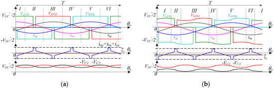
Figure 5.
Averaged-value in, iabcg, Vc1, Vc2, and ViTTR. (a) Balanced DC bus voltages, and (b) unbalanced DC bus voltages.
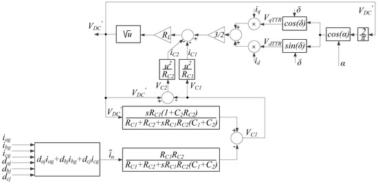
Figure 6.
Block diagram of the Vienna rectifier model.
A non-null average leads to unbalanced DC bus voltages [16,17,18]; moreover, the mean value of fundamental voltages Va1TTR becomes negative if VC1 < VC2 or positive if VC2 < VC1. This is included in the TTR model by adding the term ΔVDC′ = VC1 − VC2:
According to Table 2, by replacing (21) into (20), is given by
3.3. TLI Model
A key task of the TLI present in the AHUTR topology is to compensate all low-order voltage harmonics generated by the step-modulated Vienna rectifier [12]. For this reason, the TLI reference phase voltage is equal to the difference between the AC side input voltage ViTTR and its fundamental component Vi1TTR, as shown in Figure 7.
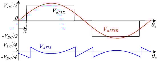
Figure 7.
Two-level inverter (TLI) reference voltage for active power filtering.
Phase voltages ViTTR encompass some zero sequence components, such as the 3rd, 9th, 27th, and 81st, that will not result in corresponding currents in the PMSG because the considered open-end winding topology is composed by two isolated converters. Hence, these harmonics can be neglected in the TLI reference voltages ViTLI*. This leads to a reduction of TLI DC bus voltage and, accordingly, to a positive impact on TLI losses. TLI reference voltages VabcTLI* are thus given by
Figure 8 shows the VaTLI* waveform when considering a different set of zero sequence components. For each case, the minimum VDC″/VDC′ requirement has been computed as shown in Figure 9, while current and voltage THDs are provided in Figure 10. At medium-high values of the modulation index mTTR, a proper suppression of the effects of the low-order voltage harmonics produced by the Vienna rectifier is simply achieved by compensating the 5th and 7th harmonics. However, at low mTTR, additional harmonics must be considered to keep the THDs suitably low.
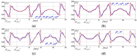
Figure 8.
TLI reference voltage approximation. (a) 3rd, 5th, 7th, 9th, 11th, 13th. (b) 5th, 7th, 11th, 13th. (c) 5th, 7th, 11th. (d) 5th, 7th.
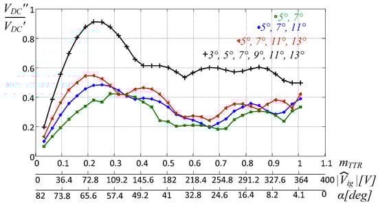
Figure 9.
Minimum VDC″/VDC′ requirement vs. peak amplitude of PMSG phase voltage, mTTR, and α.
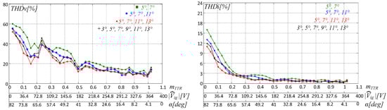
Figure 10.
THDv and THDi vs. the peak amplitude of PMSG phase voltage.
As shown in Figure 2, a closed loop input current control system is added to the predictive filter in order to cope with unmodeled non-linearities and improve the input current waveform as well as the system dynamic response. By equaling the active power generated by the PMSG to the output DC power, the reference q-axis current iq* is computed from actual values of α, δ and the output DC current iDC as:
The d-axis reference current id* can be simply set to zero or suitably determined in case of interior permanent magnet structures in order to operate the PMSG according to a maximum power per ampere strategy.
Another key function of the TLI is to balance the voltage across the DC bus capacitors of the Vienna rectifier, making unnecessary additional circuits. As shown in Figure 2, this goal is obtained by acting on the q-axis component of the TLI reference current in order to control the amplitude of in, which is given by the difference between the currents flowing through the two DC bus capacitors.
The DC side of the TLI is modeled by balancing the AC and DC side power, neglecting the power switches losses (Equation (26)). The TLI DC-link includes the resistance RCT representing the floating capacitor losses, while VqTLI and VdTLI are the voltage components of TLI VjTLI in the qd axis, as shown in Figure 11.
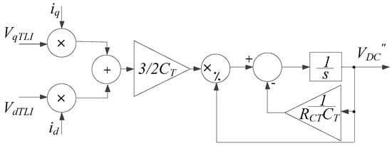
Figure 11.
Block diagram of TLI model.
4. Model Validation
An electric power generation application has been considered for validating the value-averaged model. Specifically, the proposed model represented with the blocks scheme of Figure 12 has been implemented in a Simulink environment and compared to a detailed model of the system developed in the same environment exploiting the SimPower System Toolbox, which is a circuit-based modeling platform widely used for the simulation of power electronic converters, electromechanical systems, and their control systems. The last model includes both converter topologies. The control scheme used on both models is shown in Figure 2, including low-order harmonic compensation and DC bus capacitor voltages balancing [14]. Simulation settings are summarized in Table 3, where kPα and kIα are the proportional and integral gains of the output DC voltage controller, while kPiq, kIiq, kPid, and kIid are the proportional and integral gains of qd PMSG current regulators; kPin and kIin are the proportional and integral gains of the Vienna rectifier DC bus voltage equalization system; and kPTLI and kITLI are the proportional and integral gains of the TLI DC Bus voltage controller. Figure 13 and Figure 14 show simulation results obtained with the SimPower System model and the averaged-value model, showing a purposely generated Vienna rectifier DC bus voltage unbalance with the balance system not activated. Specifically, capacitor voltages VC1 and VC2, which at the beginning are equal because RC1 and RC2 are both set to 1000 Ω, diverge after t = 3 s because RC2 is changed to 600Ω in order to generate the voltage unbalance. The in current is zero when capacitor voltages are balanced and greater than zero after t = 3 s, while DC bus voltages VDC′ and VDC″ do not vary. A zoomed-in view of the balanced and unbalanced steady-state operations of Figure 13 and Figure 14 are shown in Figure 15 and Figure 16, confirming a good matching between the results obtained with the two models. Figure 15d and Figure 16d show the instantaneous Vienna rectifier power losses PTTR, TLI power losses PTLI, and PMSG power losses PLg during balanced DC bus capacitors. A one-time variation of the references of the output voltage and the TLI DC bus voltage is considered in Figure 17 and Figure 18, while a load variation is shown in Figure 19 and Figure 20. The results achieved with the two models are very close, but using the averaged-value model, the simulation time is roughly one third. In particular, all simulations have been accomplished on an Intel® CoreTM i7 CPU with 2.60 GHz and 16 GB RAM running a 64-bit Windows 10 operating system. Simulation results shown in Figure 13, Figure 14, Figure 15, Figure 16, Figure 17, Figure 18, Figure 19 and Figure 20 required three minutes computing time using the SimPower System model with a 10−6 s time step. A 10−5 s time step can be used with the averaged-value model, because high frequency voltage and current harmonics are neglected, leading to only ten seconds to accomplish the same simulation.
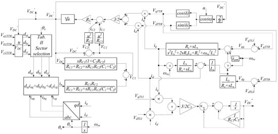
Figure 12.
Block diagram of the developed averaged-value model.
Table 3.
System parameters.
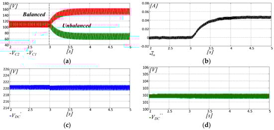
Figure 13.
SimPower System model. (a) DC bus capacitor voltages VC1 and VC2. (b) in= iC1 − iC2. (c) output voltage VDC′. (d) TLI DC bus voltage VDC″.
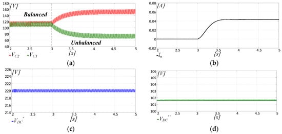
Figure 14.
Averaged-value model. (a) DC bus capacitor voltages VC1 and VC2. (b) in= iC1 − iC2. (c) output voltage VDC′. (d) TLI DC bus voltage VDC″.
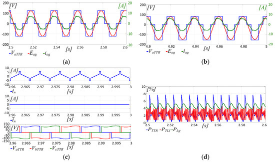
Figure 15.
SimPower System model. (a) Balanced DC bus capacitor voltage operations, VaTTR, Eag, and iag. (b) Unbalanced DC bus capacitor voltage operations. (c) Current in, average value , and AC input Vienna voltages ViTTR. (d) TRR power losses PTTR, TLI power losses PTLI, and PMSG power losses PLg.
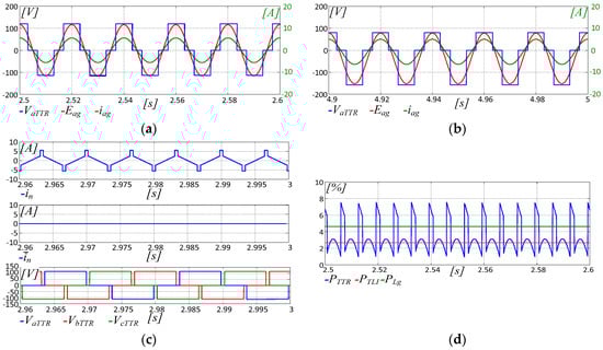
Figure 16.
Averaged-value model. (a) Balanced DC bus capacitor voltage operations, VaTTR, Eag, and iag. (b) Unbalanced DC bus capacitor voltage operations. (c) Current in, average value , and AC input Vienna voltages ViTTR. (d) TRR power losses PTTR, TLI power losses PTLI, and PMSG power losses PLg.
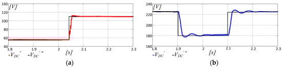
Figure 17.
SimPower System model. One-time variation of VDC′ and VDC″ references. (a) TLI DC bus voltage VDC″. (b) Output voltage VDC′.
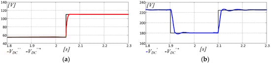
Figure 18.
Averaged-value model. One-time variation of VDC′ and VDC″ references. (a) TLI DC bus voltage VDC″. (b) Output voltage VDC′.
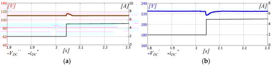
Figure 19.
SimPower System model. Load variation iDC*. (a) TLI DC bus voltage VDC″. (b) Output voltage VDC′.
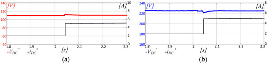
Figure 20.
Averaged-value model. Load variation iDC*. (a) TLI DC bus voltage VDC″. (b) Output voltage VDC′.
Figure 21 displays the maximum errors between the quantities carried out by the two models, confirming a good accuracy of the proposed average model in a wide range of load conditions.
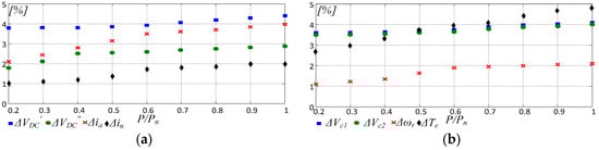
Figure 21.
Percentage error between SymPower System and averaged model vs. the power expressed in per unit P/Pn. (a) Errors of VDC′, VDC″, ia, and in. (b) Errors of Vc1, Vc2, ωr and Te. Note: ωr = 200 rad/s, VDC′ = 400 V, and VDC″ = 100 V.
5. Experimental Assessment
The accuracy of the AHUTR analytical model has also been verified comparing the results from the model with those from an experimental test rig consisting of 1kW AHUTR supplying an open-end-winding PMSG, mechanically coupled to a 2.6 kW PM synchronous motor drive used as a prime mover. Technical specifications of the PMSG are given in Table 4. This AHUTR supplied DC loads at 400V through the Vienna rectifier equipped with insulated gate bipolar transistors (IGBTs) whose technical data are listed in Table 5. The TLI was realized with low-voltage power metal-oxide-semiconductor field-effect transistor (MOSFETs) and operated at 40 kHz, VDC″ = 100 V. Technical data of the power MOSFETs are reported in Table 6. The TLI floating capacitor and both capacitors C1, C2 were equal to 470µF. The DC load was modified using a variable power resistor. A single dSPACE DS1103 control board was used to control the Vienna rectifier and the TLI, while a 2048 ppr encoder was used to measure the rotor position θr of the PMSG. The experimental setup is shown in Figure 22. The currents and voltages were measured by using a dedicated sensing board equipped with the current transducer LEM LA 55-P and voltage transducer LEM LV 25-P.
Table 4.
PMSG technical data.
Table 5.
Technical specifications of STGW30NC60KD IGBT.
Table 6.
Technical specifications of IRFB5615PBF MOSFET.
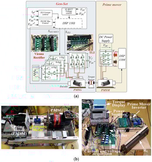
Figure 22.
Experimental test bench. (a) Block scheme. (b) Experimental setup.
The experimental results shown in Figure 23 were obtained by imposing a transient voltage to VDC′ from 400 V to 320 V by keeping a constant resistor value RL = 80 Ω and with the PMSG spinning at ωr = 200 rad/s. Note a satisfying accuracy in the mechanical and electrical quantities estimated by the model. The voltage VDC″ was properly modified by the control algorithm in order to keep the optimal ratio between the DC bus voltages VDC′ and VDC″. A different test is displayed in Figure 24 in which a speed transient was forced by acting on the prime mover. More specifically, the rotational speed ωr was changed from 200 rad/s to 260 rad/s while the resistive load was still kept constant. Even in this case, the model accurately predicted the behavior of the drive, both at steady-state and transient. The DC bus voltages were both affected by the speed variation, but the feedback control loops restored the reference values. A step load variation was imposed in the test of Figure 25, where the DC load was purposely doubled by switching from TL = 2 Nm to TL = 4 Nm. In this case, a more remarkable difference was observed between the model and the experimental results. Finally, the effectiveness of the model to predict the balancing of the voltages across the DC bus capacitors is shown in Figure 26. Initially, the balancing algorithm described in the previous sections was inactive, and thus, the voltages at the terminals of C1 and C2 were significantly different. At the instant t*, the voltage-balancing approach was activated, nullifying VC1 − VC2. The results of Figure 26 confirm the capability of the model to accurately simulate even this critical issue of the AHUTR. Maximum percentage errors between the outputs of the SimPower System and the averaged-value model are summarized in Table 7, where the quantities with the suffix Δ are the errors in estimating VDC′, ωr, Te, VDC’’, in, Vc1, and Vc2.
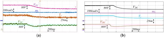
Figure 23.
Voltage transient of VDC′ from 400 V to 320 V under a constant resistor value RL = 80 Ω. Output voltage VDC′, TLI DC bus voltage VDC″, rotor speed ωr, electromagnetic torque Te. (a) Experimental results. (b) Simulation results.
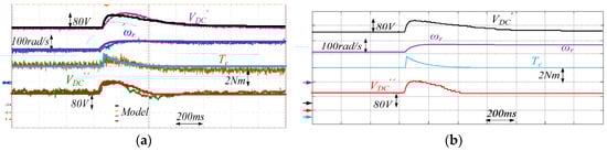
Figure 24.
Speed transient from ωr = 200 rad/s to ωr = 260 rad/s under a constant resistor value RL = 80 Ω and VDC′ = 400 V, VDC″= 100 V. Output voltage VDC′, TLI DC bus voltage VDC″, rotor speed ωr, electromagnetic torque Te. (a) Experimental results. (b) Simulation results.
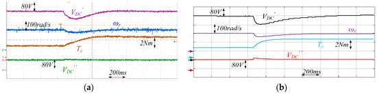
Figure 25.
Load transient from TL = 2 Nm to TL = 4 Nm at ωr = 200 rad/s and VDC′ = 400 V, VDC″ = 100 V. Output voltage VDC′, TLI DC bus voltage VDC″, rotor speed ωr, electromagnetic torque Te. (a) Experimental results. (b) Simulation results.
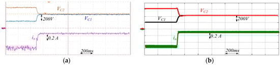
Figure 26.
DC bus voltage balancing: TL = 4 Nm, ωr = 200 rad/s and VDC′= 400 V, VDC″ = 100 V. Vc1, Vc2 and in. (a) Experimental results. (b) Simulation results.
Table 7.
Errors between experimental results and those obtained with the averaged-value model.
6. Conclusions
The asymmetrical hybrid unidirectional T-type rectifier is more efficient than a conventional PWM rectifier, mainly due to line frequency operation of the main converter, a T-type rectifier. However, it features a more complex structure composed of three main components, namely a TTR, a TLI, and an open winding electric machine, all interacting. The development of an accurate averaged-value mathematical model of the AHUTR topology aimed to optimally design control and management algorithms has been faced in the paper. Simulations and experimental results show that the proposed model is able to reproduce the static and dynamic behavior of the AHUTR with good accuracy. Furthermore, the obtained mathematical representation made a fast analysis of the system during TTR DC bus voltage unbalance operations possible. This has been exploited to design an active balancing system acting on the TLI side—a task which would be time-consuming with circuit-oriented simulator models. Furthermore, the averaged-value model has been used to define the entire AHTUR control and management system tasked to deal with efficiency maximization, input power factor control, TTR DC bus capacitor voltage balance, and the control of TLI floating DC bus voltage.
Author Contributions
This work was carried out in collaboration between all authors. S.F., G.S. and A.T. designed the study, wrote the manuscript and analyzed simulations and experimental results. A.S. undertook all of the experimental measurements.
Conflicts of Interest
The authors declare no conflict of interest.
References
- Kaarthik, R.S.; Gopakumar, K.; Mathey, J.; Underland, T. Medium Voltage Drive for Induction Machine with Multilevel Dodecagon Voltage Space Vectors with Symmetric Triangles. IEEE Trans. Ind. Electron. 2015, 62, 79–87. [Google Scholar] [CrossRef]
- Kouro, S.; Malinowski, M.; Gopakumar, K.; Pou, J.; Franquelo, L.G.; Wu, B.; Rodriguez, J.; Perez, M.A.; Leon, J.I. Recent Advances and Industrial Applications of Multilevel Converters. IEEE Trans. Ind. Electron. 2010, 57, 2553–2580. [Google Scholar] [CrossRef]
- De Caro, S.; Foti, S.; Scimone, T.; Testa, A.; Cacciato, M.; Scarcella, G.; Scelba, G. THD and efficiency improvement in multi-level inverters through an open end winding configuration. In Proceedings of the IEEE 2016 Energy Conversion Congress and Expo, Milwaukee, WI, USA, 18–22 September 2016; pp. 1–7. [Google Scholar]
- Edpuganti, A.; Rathore, A. A Survey of Low Switching Frequency Modulation Techniques for Medium-Voltage Multilevel Converters. IEEE Trans. Ind. Appl. 2015, 51, 4212–4228. [Google Scholar] [CrossRef]
- Mondal, G.; Sivakumar, K.; Ramchand, R.; Gopakumar, K.; Levi, E. A Dual Seven-Level Inverter Supply for an Open-End Winding Induction Motor Drive. IEEE Trans. Ind. Electron. 2009, 56, 1665–1673. [Google Scholar] [CrossRef]
- Wang, Y.; Panda, D.; Lipo, T.A.; Pan, D. Open-Winding Power Conversion Systems Fed by Half-Controlled Converters. IEEE Trans. on Power Electron. 2013, 28, 2427–2436. [Google Scholar] [CrossRef]
- Mohapatra, K.K.; Gopakumar, K.; Somasekhar, V.T.; Umanand, L. A Harmonic Elimination and Suppression Scheme for an Open-End Winding Induction Motor Drive. IEEE Trans. Ind. Electron. 2003, 50, 1187–1198. [Google Scholar] [CrossRef]
- Kawabata, Y.; Nasu, M.; Nomoto, T.; Ejiogu, E.C.; Kawabata, T. High-efficiency and low acoustic noise drive system using open-winding AC motor and two space-vector-modulated inverters. IEEE Trans. Ind. Electron. 2002, 49, 783–789. [Google Scholar] [CrossRef]
- Sivakumar, K.; Das, A.; Ramchand, R.; Patel, C.; Gopakumar, K. A hybrid multilevel inverter topology for an open-end winding induction-motor drive using two-level inverters in series with a capacitor-fed H- bridge cell. IEEE Trans. Ind. Electron. 2010, 57, 3707–3714. [Google Scholar] [CrossRef]
- Somasekhar, V.T.; Gopakumar, K.; Bajiu, M.R.; Mohapatra, K.K.; Umanand, L. A multilevel inverter system for an inductor motor with open-end windings. IEEE Trans. Ind. Electron. 2015, 52, 824–836. [Google Scholar] [CrossRef]
- Edpuganti, A.; Rathore, A.K. Optimal Pulsewidth Modulation for Common-Mode Voltage Elimination Scheme of Medium-Voltage Modular Multilevel Converter-Fed Open-End Stator Winding Induction Motor Drives. IEEE Trans. Ind. Electron. 2017, 64, 848–856. [Google Scholar] [CrossRef]
- Foti, S.; Testa, A.; Scelba, G.; De Caro, S.; Cacciato, M.; Scarcella, G.; Scimone, T. An Open-End Winding Motor Approach to Mitigate the Phase Voltage Distortion on Multilevel Inverters. IEEE Trans. Power Electron. 2018, 33, 2404–2416. [Google Scholar] [CrossRef]
- Foti, S.; Testa, A.; Scelba, G.; Sabatini, V.; Lidozzi, A.; Solero, L. A symmetrical hybrid unidirectional T-type rectifier for high-speed gen-set applications. In Proceedings of the IEEE Energy Conversion Congress and Expo, Cincinnati, OH, USA, 1–5 October 2017; pp. 4887–4893. [Google Scholar]
- Foti, S.; De Caro, S.; Scelba, G.; Scimone, T.; Testa, A.; Cacciato, M.; Scarcella, G. An Optimal Current Control Strategy for Asymmetrical Hybrid Multilevel Inverters. IEEE Trans. Ind. Appl. 2018, 54, 4425–4436. [Google Scholar] [CrossRef]
- Mengoni, M.; Amerise, A.; Zarri, L.; Tani, A.; Serra, G.; Casadei, D. Control Scheme for Open-Ended Induction Motor Drives with a Floating Capacitor Bridge Over a Wide Speed Range. Trans. Ind. Applications 2017, 53, 4504–4514. [Google Scholar] [CrossRef]
- Pan, Z.; Peng, F.Z.; Corzine, K.A.; Stefanovic, V.R.; Leuthen, J.M.; Gataric, S. Voltage balancing control of diode-clamped multilevel rectifier/inverter systems. IEEE Trans. Ind. Applications 2005, 41, 1698–1706. [Google Scholar] [CrossRef]
- Yan, G.; Duan, S.; Zhao, S.; Li, G.; Wu, W.; Li, H. Research on the mechanism of neutral-point voltage fluctuation and capacitor voltage balancing control strategy of three-phase three-level T-type inverter. J. Electr. Eng. Technol. 2017, 12, 2227–2236. [Google Scholar]
- Zhang, Y.; Li, J.; Li, X.; Cao, Y.; Sumner, M.; Xia, C. A Method for the Suppression of Fluctuations in the Neutral-Point Potential of a Three-Level NPC Inverter with a Capacitor-Voltage Loop. IEEE Trans. Power Electron. 2017, 32, 825–836. [Google Scholar] [CrossRef]
© 2019 by the authors. Licensee MDPI, Basel, Switzerland. This article is an open access article distributed under the terms and conditions of the Creative Commons Attribution (CC BY) license (http://creativecommons.org/licenses/by/4.0/).