Thin Film on CMOS Active Pixel Sensor for Space Applications

Abstract
:
1. Introduction
2. Results and Discussion
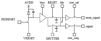
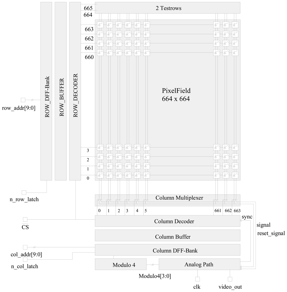
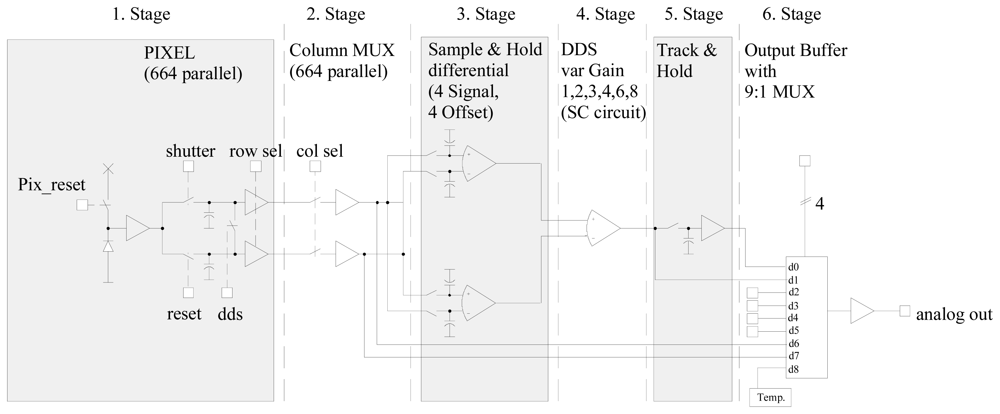
2.1. CMOS circuit architecture
2.2. Thin Film on CMOS (TFC) Technology
3. Results
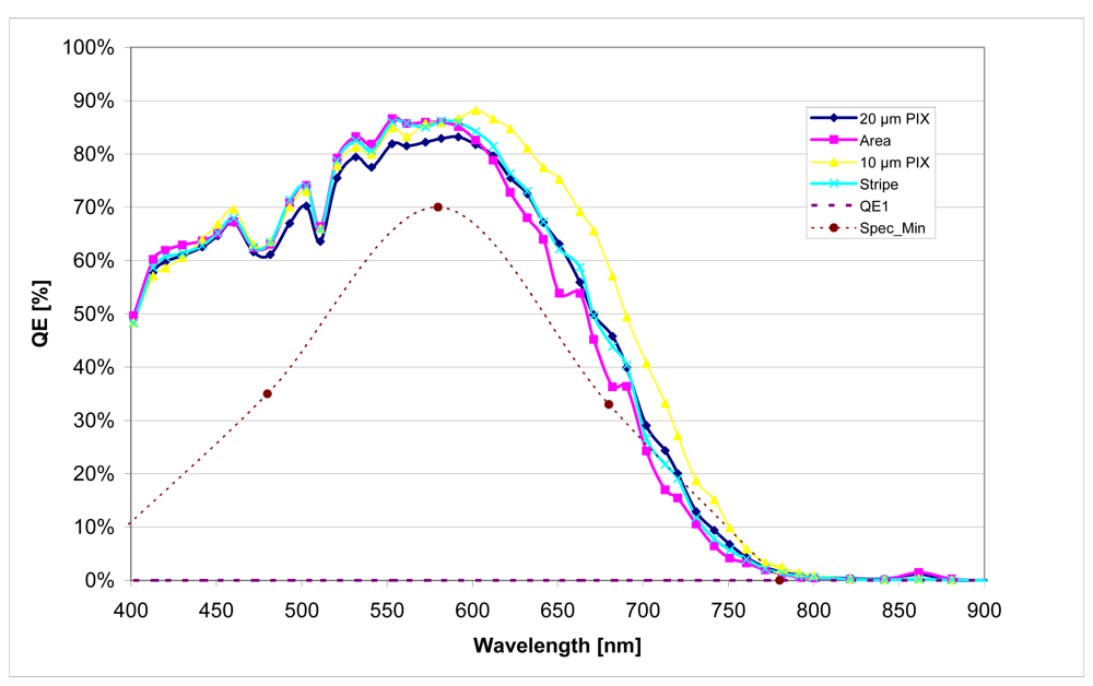
3.1. Characterization of the CMOS circuitry without TFC layer
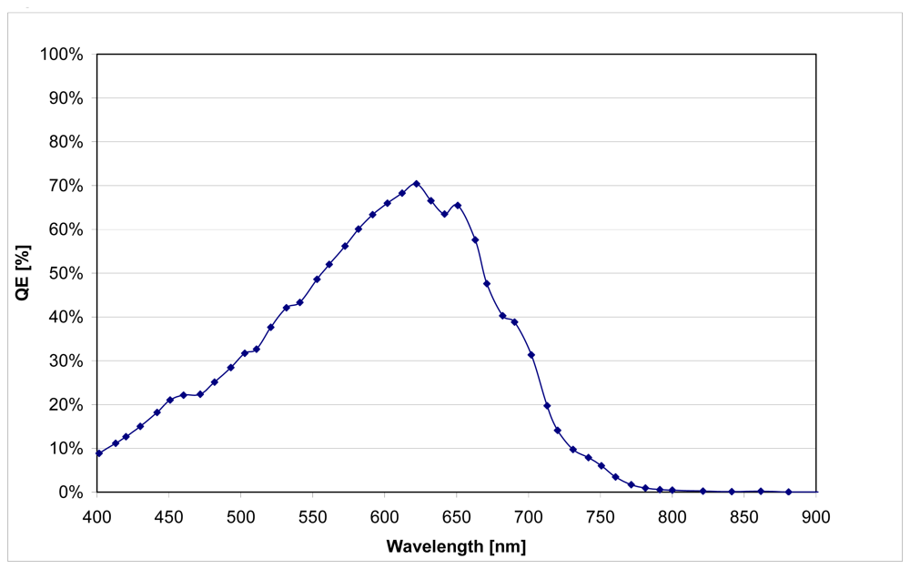
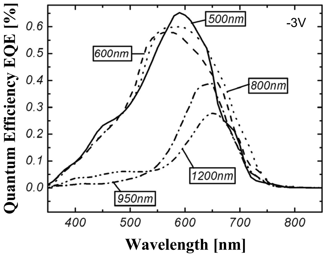
3.2. Measurements of the TFC layer
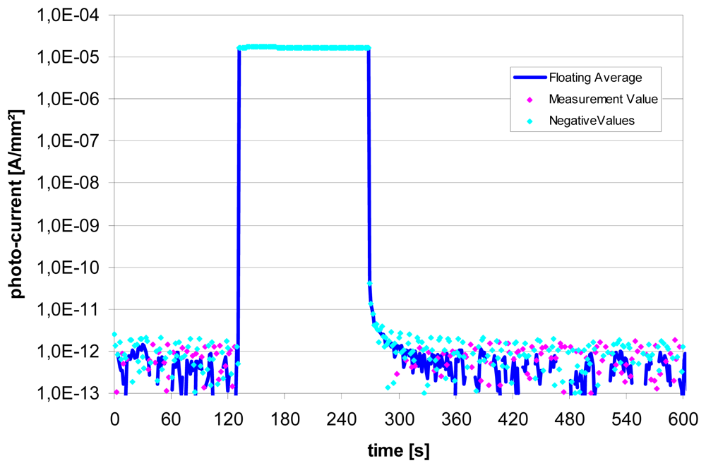
3.3. Irradiation tests
4. Conclusions
Acknowledgments
References
- Bogaerts, J.; Dierickx, B.; Meynants, G.; Uwaerts, D. Total dose and displacement damage effects in a radiation-hardened CMOS APS. IEEE Trans. Nucl. Sci. 2002, 49, 1513–1521. [Google Scholar]
- Cypress Semiconductor Corperation. STAR1000 1M Pixel Radiation Hard CMOS Image Sensor. Datasheet STAR1000 2006, 38-05714(*B), 1–21. [Google Scholar]
- Kataoka, S. Three-Dimensional Integrated Sensors. Proc. IEDM ′86 1986, 361–364. [Google Scholar]
- Schneider, B.; Fischer, H.; Benthien, S.; Keller, H.; Lulé, T.; Rieve, P.; Sommer, M.; Schulte, J.; Böhm, M. TFA Image Sensors: From the One Transistor Cell to a locally adaptive High Dynamic Range Sensor. Proc. IEDM 1997, 209–212. [Google Scholar]
- Harendt, C.; Graf, H.G.; Schubert, M.B. Logarithmic HDRC Image Sensors with Thin-Film-on-CMOS Technology. 1st Fraunhofer Workshop on CMOS-Imaging, From Technology to Application, Duisburg, Germany, May 2002.
- Moussy, N.; Gidon, P.; Carrière, N.; Rabaud, W.; Giffard, B.; Glück, B.; Thomas, D.; Prima, J.; Roy, F.; Casanova, N.; Regolini, J.; Chevrier, J.B.; Collet, F.; Ozanne-Gomilla, A.S.; Salasca, O. A highly reliable amorphous photosensor for above IC CMOS image sensors. Proc. IEDM 2006, 209–212. [Google Scholar]
- White, M.W.; Lampe, D.R.; Blaha, F.C.; Mack, I.A. Characterization of surface channel CCD image arrays at low light level. IEEE JSSC 1974, 9, 1–13. [Google Scholar]
- Weste, N.H.E.; Eshraghian, K. Principles of CMOS VLSI Design: A Perspective., 1st Ed. ed; Addison Wesley: Boston, USA, 1985; pp. 58–60. [Google Scholar]
- Hastings, A. The Art of Analog Layout., 1st Ed. ed; Prentice Hall: New Jersey, USA, 2001; pp. 375–376. [Google Scholar]
- Neidlinger, T.; Harendt, C.; Glöckner, J.; Schubert, M.B. Novel device concept for voltage-bias controlled color detection in amorphous silicon based CMOS cameras. Mat. Res. Soc. Symp Proc. 1999, 558, 285. [Google Scholar]
- Neidlinger, T.; Schubert, M.B.; Schmid, G.; Brummack, H. Fast Color Detection with Two- Terminal P-I-I-N Devices. Mat. Res. Soc. Symp. Proc. 1996, 420, 147. [Google Scholar]
- Pieters, B.E.; Krc, J.; Zeman, Z. Advanced numerical simulation tool for solar cells-ASA5. Conference Record of the 2006 IEEE 4th World Conference on Photovoltaic Energy Conversion; 2006; Volume 2, pp. 1513–1516. [Google Scholar]


| TFC Layer Thickness [μm] | Star Magnitude 1 | Star Magnitude 6 | Saturation Charge [e-] | Capacitance Linearity [%] | ||||
|---|---|---|---|---|---|---|---|---|
| Signal @ 0.1s integr. [e-] | Noise @ 0.1s integr. [e-] | S/N at 10 bit A/D [dB] | Signal @ 0.1s integr. [e-] | Noise @ 0.1s integr. [e-] | S/N at 10 bit A/D [dB] | |||
| 0.5 | 121200 | 498 | 47 | 1882 | 358 | 10 | 500000 | 99.2 |
| 1.0 | 143960 | 426 | 50 | 1610 | 199 | 13 | 272232 | 98.6 |
| 1.5 | 155220 | 418 | 50 | 1713 | 147 | 19 | 197109 | 98.1 |
| 1.8 | 159950 | 418 | 50 | 1759 | 130 | 19 | 172018 | 97.8 |
| 2.0 | 162400 | 419 | 50 | 1784 | 122 | 19 | 159575 | 97.6 |
| 2.2 | 164550 | 420 | 50 | 1807 | 115 | 19 | 149254 | 97.5 |
| N° | Characteristics | Limits | Unit | ||||||
|---|---|---|---|---|---|---|---|---|---|
| Min | Typ | Max | |||||||
| 1. | Signal Generation | integrating | - | ||||||
| 2. | Shutter | full field synchronous | - | ||||||
| 3. | Pixel Access | XY random pixel access | - | ||||||
| 4. | Pixel Signal Read-Out | multiple non-destructive | - | ||||||
| 5. | Power Supply | single voltage supply (+5V) | - | ||||||
| 6. | Array Size | 640 × 640 | pixel | ||||||
| 7. | Pixel Pitch | 20 × 20 | μm | ||||||
| 8. | Fill Factor | 85 | 100 | % | |||||
| 9. | Full Well Capacity | 112000 | 140000 | e- | |||||
| 10. | Sensitivity | 10 (dynamic: 1:1000) | |||||||
| 11. | Exposure Time | 0.1 | 1000 | ms | |||||
| 12. | Non Linearity up to Full Well | 5 | 10 | % | |||||
| 13. | Dark Signal @ 293°K | 80 | pA/cm2 | ||||||
| 14. | DSNU (1σ Full Well ) | 5 * | % | ||||||
| 15. | PRNU (1σ 90% Full Well ) | 9 * | % | ||||||
| 16. | Power Consumption | 850 | mW | ||||||
| 17. | Signal Frequency | 5 | 10 | MHz | |||||
| * With CDS and DDS | |||||||||
© 2008 by the authors; licensee Molecular Diversity Preservation International, Basel, Switzerland. This article is an open-access article distributed under the terms and conditions of the Creative Commons Attribution license (http://creativecommons.org/licenses/by/3.0/).
Share and Cite
Schulze Spuentrup, J.D.; Burghartz, J.N.; Graf, H.-G.; Harendt, C.; Hutter, F.; Nicke, M.; Schmidt, U.; Schubert, M.; Sterzel, J. Thin Film on CMOS Active Pixel Sensor for Space Applications. Sensors 2008, 8, 6340-6354. https://doi.org/10.3390/s8106340
Schulze Spuentrup JD, Burghartz JN, Graf H-G, Harendt C, Hutter F, Nicke M, Schmidt U, Schubert M, Sterzel J. Thin Film on CMOS Active Pixel Sensor for Space Applications. Sensors. 2008; 8(10):6340-6354. https://doi.org/10.3390/s8106340
Chicago/Turabian StyleSchulze Spuentrup, Jan Dirk, Joachim N. Burghartz, Heinz-Gerd Graf, Christine Harendt, Franz Hutter, Markus Nicke, Uwe Schmidt, Markus Schubert, and Juergen Sterzel. 2008. "Thin Film on CMOS Active Pixel Sensor for Space Applications" Sensors 8, no. 10: 6340-6354. https://doi.org/10.3390/s8106340
APA StyleSchulze Spuentrup, J. D., Burghartz, J. N., Graf, H.-G., Harendt, C., Hutter, F., Nicke, M., Schmidt, U., Schubert, M., & Sterzel, J. (2008). Thin Film on CMOS Active Pixel Sensor for Space Applications. Sensors, 8(10), 6340-6354. https://doi.org/10.3390/s8106340