1. Introduction
Chemical gas sensors usually utilize an electrical or optical response by adsorption of gas molecules on surface of an active layer. Among them metal-oxide gas sensors [
1-
3] are a representative example. The metal-oxide gas sensors consist of SnO
2, ZnO or TiO
2, as active layer, where the adsorption of gas molecules leads to a large change in its electrical resistivity. They have merits of low cost, good sensitivity, and convenient form of response (a simple change in resistance). But in order to achieve enhanced chemical reactivity between gas molecules and active layer, the sensors need to drive at high temperature of 200-500°C which causes problems of high power consumption and pre-heating time. Otherwise, some gas sensors which enable to operate even at room temperature have ever been developed with no metal-oxide like porous silicon [
4-
5]. However, all gas-adsorptive types of sensors have still potential difficulties in detecting gases with low adsorption energy or low electronegativity toward the active layer, among other limitations.
By the way, ionization sensors [
6-
8] which can detect gas molecules, regardless of the magnitude of the gas adsorption energy, have been deployed for a variety of applications such as environmental monitoring, sensing in chemical processing plants, and gas detection for counter-terrorism. They work by fingerprinting ionization characteristics of distinct gases. Generally the hot-cathode type of ionization sensors has been more prevailed due to easy thermionic emission of electrons from a cathode than the cold-cathode type by field emission, but the thermionic emission has some weak points; as pressure is very sensitive to temperature, the heat from filament must be blocked, and as chemical reaction by heated filament leads to additional contribution to the concentration, it must be restricted. Besides, all of the ionization sensors are limited by their huge and bulky architecture, high power consumption and risky high-voltage operation as they can be little fabricated by typical semiconductor process. If standard batch processing, as in the IC industry, is applicable to manufacturing sensors, a lot of identical sensors will be produced in one run, thus substantially improving their performance/cost ratio. Additionally, the miniaturization of sensors will not only contribute to their potentially low cost, but also allow them to be integrated with microelectronic circuits; thus, further enhancing their performance.
Here we propose a sensor differentiated from past ionization sensors [
6-
8] by its small size and by processes used in its manufacture. Recently, carbon nanotube(CNT)-based sensors which may be classified into chemical and physical types for convenience have been developed for gas detection. Early chemical types of CNT sensors were reported in some journals [
9-
12]. They usually figured out the data with the changes of conductivity and permittivity in CNTs by gas adsorption, and have shown merits such as good electrical response even at room temperature as well as a small size.
On the other hand, physical types of CNT gas sensors [
13-
14] were later introduced which utilized ionization of neutral gas by collisions with electrons under highly applied voltage. In general, physical gas sensors should be strong to high-voltage application. CNTs have relatively low electron escaping work and very sharp tip curvatures, and remain structurally stable under high electric fields [
15], so the CNTs have been known to be the best field emitters over conventional field emitting metals such as Mo and W. Further, it has been known that vertically aligned CNT array covering a cathode is more compatible to produce a consistent nanometer-scale surface topology than conventional planar electrodes or micro-machined electron emitters. Therefore the CNT array is expected as a good cathode for electron emission, leading to dark discharge current more effectively.
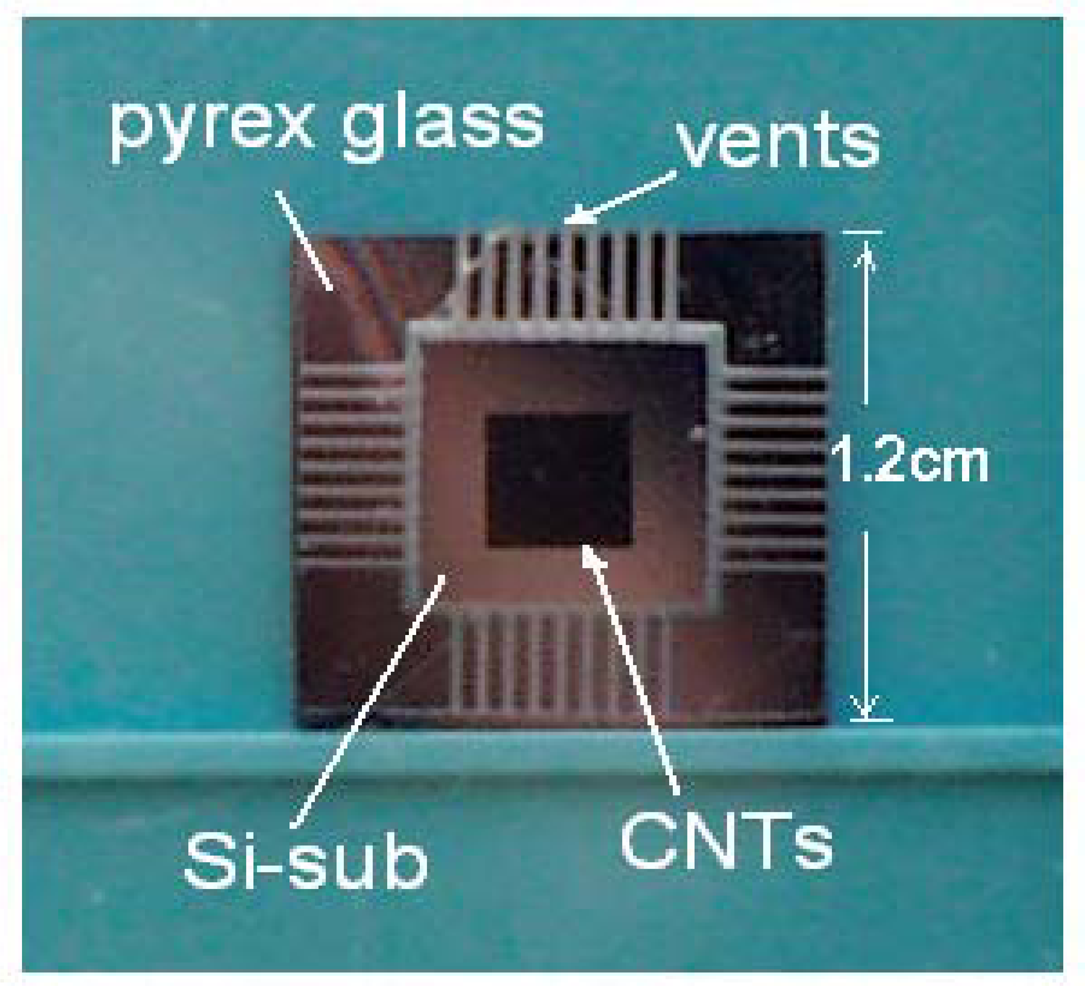
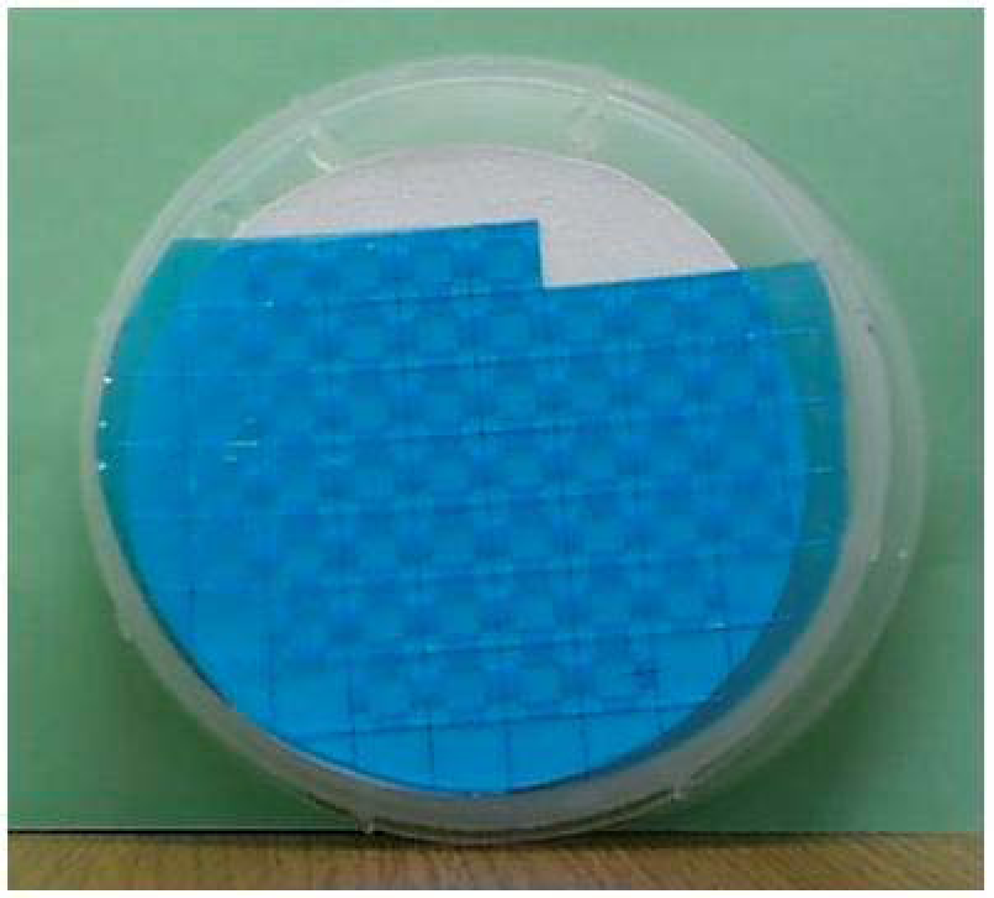
In this paper, we introduced efficient process for fabricating CNT sensors with simplicity and compactness in the structure and reliability in process, inspected I-V properties in the dark discharge region with the sensors, and discussed the results with well-known Paschen's curves.
3. Results and Discussion
Even though most gases in a chamber remain predominantly neutral in electricity, they can produce spontaneously a small number of electrons and ions by cosmic rays and natural radioactivity. Once these generated electrons and ions will move if a static voltage is applied; that is, electrons will migrate to an anode, ions to a cathode, and a small current will flow between two electrodes. But this current has no visible effects, and can be detected and measured only with difficulty because of small quantity in electrical charges.
By the electrical discharge theory in ideal gas, the typical discharge I-V curve is shaped as shown in
Figure 5. When the applied voltage between an anode and a cathode is given as V= V
o- IR where V
o is the voltage supplied from the power supply, the I-V curve is divided to three parts and the operating point on the curve is determined by a load line according to values of the resistance,
R. If operating point A is placed in a dark discharge region as shown in the figure, the current is no more than hundreds microampere, and is not self-sustained. If the applied voltage is increased or the resistance is reduced further, operating point A will move up the curve until the sparking voltage,
Vs, is reached. And then the voltage applied to the sensor is sharply reduced, the operating point is transited to a glow discharge region, and the discharge is now self-sustained. If the resistance,
R, is changed to a much smaller value in the glow discharge region, cathode heating may be enough to increase the electron supply and lower the discharge voltage, and the operating point will be transited to an arc region. Therefore, the transit of the operating point to other region on the discharge I-V curve is possible by controlling the applied voltage or the resistance.
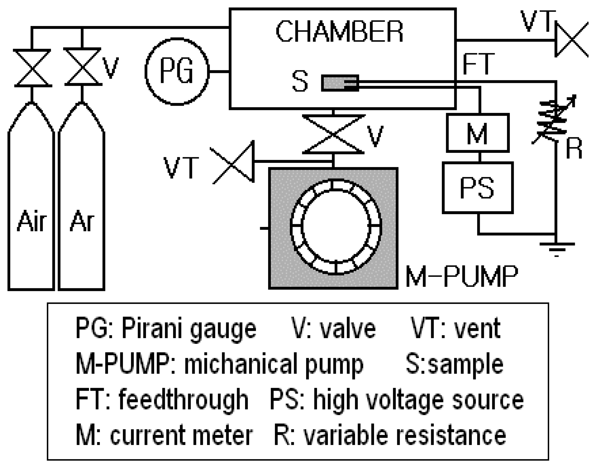
In this work, the operating point of the sensor is limited only within the dark discharge region by connecting in series with a current-limiting resistance and by restricting the maximum applied voltage to 1kV.
We assume that the medium in the chamber is an ideal gas and that electrons are emitted from the micro tips of the vertically aligned CNT array under high applied voltage. Once electrons are emitted from the CNT array, they are accelerated towards the anode by electrical field, collide with gas molecules, and lead to the ionization of these neural molecules. Therefore, I-V characteristics in the dark discharge region depend both on the amount of electrons and positive ions generated through collisions and on the drift velocity of the electrons.
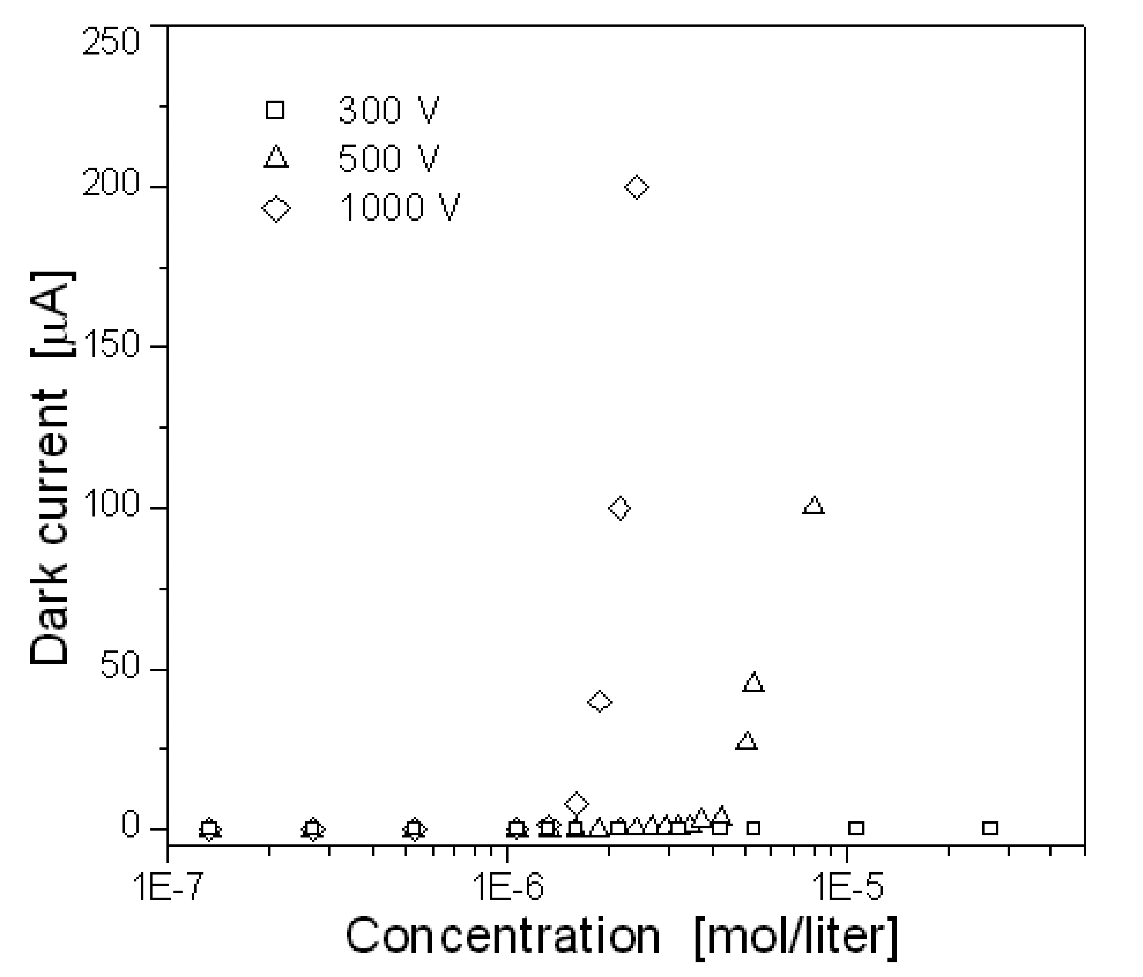
Figure 6 shows the dependence of the dark current on air concentration in the chamber under the applied voltages of 300, 500 and 1000V, where the concentration is defined as the unit of mol/liter and the distance between the electrodes is constant about 500μm. As shown in the figure, the current increased with the applied voltage by the increase of the drift velocity, and it was found that the current increased abruptly over some critical concentrations on the voltages of 500 and 1000V, while any abruption in the current did not occur regardless of the concentration below the low applied voltage like 300V. That is, there existed a minimum voltage to cause a cascading of secondary electrons, since the electron energy gain is proportional to electrical field.
In summary, the dark current increased with the air concentration because more charges could be generated by collision, and the abruptions in current were shifted to the lower concentration as the static voltage increased higher. At 500V the current abruption occurred at 5×10⁻⁶ mol/liter, while at 1000V it occurred at 1.5×10⁻⁶ mol/liter.
In this work, we explain a detection process of the gas concentration and identity by ionization theoretically with Paschen's law. Paschen's law reflects a dark discharge mechanism, that is, a cascading of secondary electrons emitted by collisions in a gap, where the initial sparking breakdown voltage,
Vs, is decided by a function of the product of the gas pressure,
p, and the distance between two electrodes,
d, and is expressed as
In this experiment, the breakdown voltage depends only on the pressure because the distance between the anode and the cathode is constant.
Paschen's law can be visualized graphically, where the curves show the lowest breakdown voltage to be roughly an order of magnitude larger than the ionization voltage. Starting from low pressure, the breakdown voltage at first decreases with increasing pressure because more molecules can be ionized, but at higher pressure the breakdown voltage increases with pressure because the mean free path decreases and electrons have difficulty reaching ionization energy.
By the way, the conversion from pressure to concentration can be derived by the state equation for ideal gas;
where p is the pressure, n the concentration expressed as the number of moles of gas per unit volume, R the ideal gas constant, and T the absolute temperature.
An electron can ionize neutral atoms by collision with the energy required to free the least bound electron from an atom being the ionization energy. If the gas concentration changes, other parameters remaining constant, production of electron-ion pairs will change correspondingly.
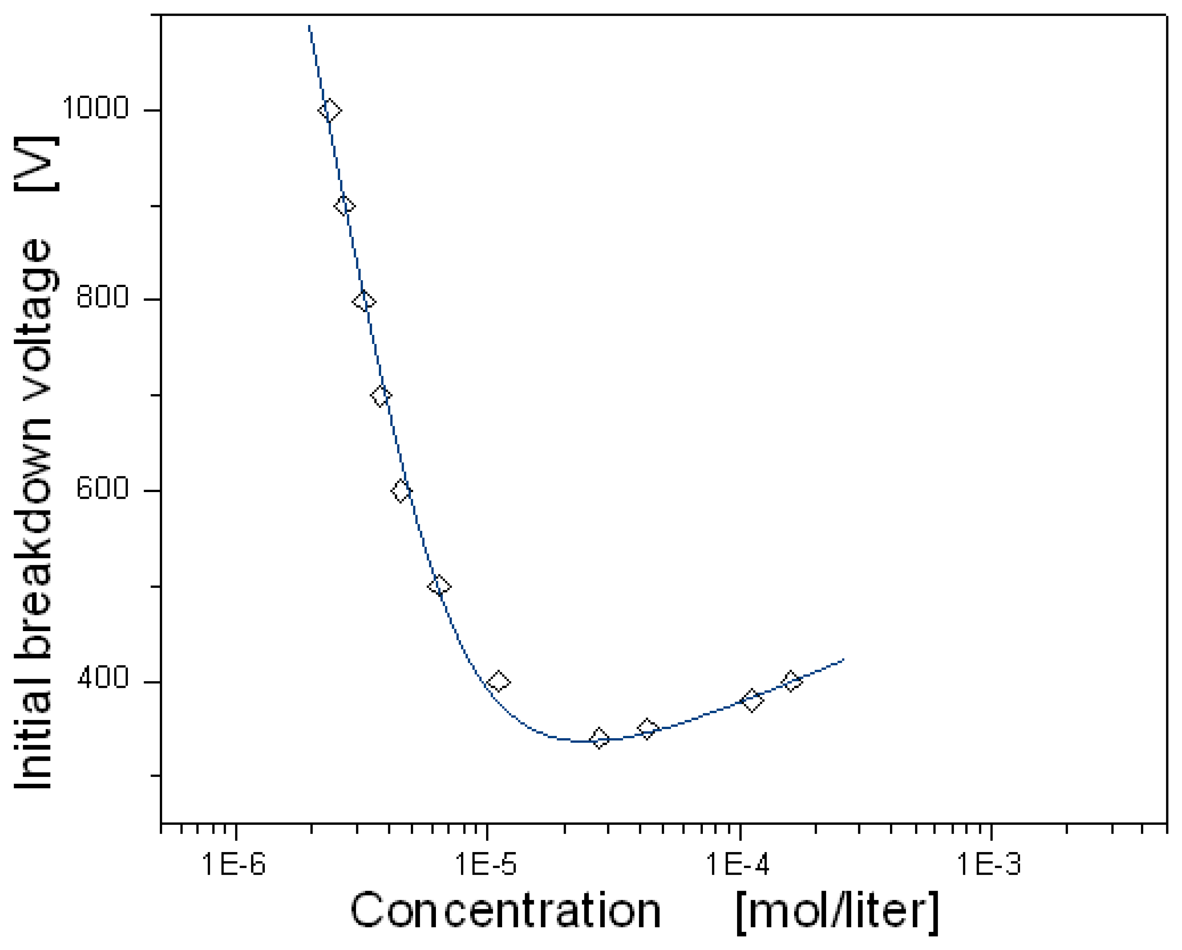
Figure 7 shows the dependence of the initial breakdown voltage on air concentration in the chamber. For simplification, the initial breakdown voltage was defined as the voltage necessary for 0.1mA current. On the left side of the curve indicating the lower concentration, the initial breakdown voltage was fast increased with the reduction of the concentration because the dark discharge current depends on the amount of neutral molecules in the chamber which can provide electron-ion pairs generated by collisions. However, on the right side of the curve, the initial breakdown voltage was slowly increased with the increase of the concentration. In this region, the ionization rate is predominantly determined by the length of the mean free path rather than the amount of neutral molecules. The electron energy gain between two collisions is proportional to electrical field and is inversely proportional to concentration; thus if the gas concentration is higher, the mean free path will be shorter, and then the kinetic energy of the electron is not enough to ionize the neutral molecules. Therefore, as the ionization rate by collision is reduced with the concentration, the initial breakdown voltage increases with it. For air the minimum breakdown voltage was observed to be around 340V under the condition that the distance between the electrodes was fixed to 500μm.
The ionization rate of neutral molecules depends strongly on the concentration and the ionization energy of neutral molecules. Therefore the breakdown characteristics differ according to gases, and it is possible to detect the identity and the concentration of unknown gas species.
Figure 8 shows the dependence of the breakdown voltage on Ar concentration. Over the whole range of the concentration the breakdown voltage in argon was lower than air because of relatively low electronegativity, even though the ionization energy of Ar gas (15.7eV) is somewhat larger than that of nitrogen (15.5eV) or oxygen (12.6eV) gases. In general, high electronegative gases such as SF
6, Freon, oxygen, and nitrogen including air can reattach electrons after ionization easily and then turn to be neutral. Consequently, the discharge current in air is relatively reduced by the recombination, and the breakdown voltage in air becomes higher than that of Ar. The minimum breakdown voltage in Ar ambience was observed to be around 230V less than that of air.


