1. Introduction
Due to their potential optical utilization, materials such as silica (SiO
2), titania (TiO
2), and silica–titania (SiO
2-TiO
2) developed via the sol–gel method have been widely studied [
1]. They have been exploited to make planar, rib, and ridge waveguides for optical connection with good optical features and low optical transmission losses [
2,
3,
4]. The sol–gel method is straightforward and low-cost [
5]. It can be deposited in large areas and does not need to be processed at high temperatures. It permits the creation of thin films with outstanding thermal and mechanical stability as well as great optical performance. An appropriate refractive index contrast between the substrate and the guiding layer is required for a working waveguide. With the proper adjustment of the set-off precursors and solvents, in addition to the molar ratio of the compounds and the thermal treatment temperature, it is possible to fine-tune the refractive index and thickness of the films produced by the sol–gel process. These waveguides may be doped with rare-earth elements, laser dyes, and other organic compounds, allowing SiO
2 and TiO
2 materials made by the sol–gel process to be employed in optical amplifiers, laser-active media, and sensing applications [
6]. Several research groups have demonstrated optical waveguides based on the SiO
2-TiO
2 platform for a variety of eye-catching applications in recent years [
7,
8,
9,
10].
Subwavelength gratings (SWGs) have been a critical component in the fabrication of viable, high-performance integrated silicon photonics devices, for instance, low-loss fiber-to-chip couplers [
11], selective filters [
12], modulators, sensors [
13,
14], and ultra-broadband waveguide couplers [
15]. The cross-section of an SWG waveguide is equivalent to that of a ridge waveguide, but it features periodic refractive index modulation along the propagation direction of light. Specific wavelength bands can be directed as a Bloch waveguide mode due to the periodicity of the subwavelength grating. SWG waveguide with a certain grating period or duty cycle (hereafter represented as
DC) may be well-organized for each given wavelength band to be transmitted. The SWG waveguides are appealing because they allow the modification of the guided mode’s effective index and dispersion properties [
16]. SWG waveguides are composed of periodic silicon segments that are smaller than the propagation wavelength, removing diffraction effects and acting like a typical waveguide made up of complementary birefringent material [
17]. The lithographic manipulation of the material refractive index and dispersion is possible thanks to the etched structural geometry.
EM-wave propagation in periodic media is defined by the Bloch–Floquet principle [
18]. A mode’s propagation may be divided into three wavelength areas when designed for a certain grating period (
ᴧ): (i) The wavelength regime (λ
Bragg) when the Bloch wave is leaky, and the waveguide scatters a portion of the mode power. (ii) In the wavelength range comparable to the photonic bandgap (PBG) when the frequency bands are below the diffraction zone, Bragg reflections occur. Furthermore, the propagation light cannot be phase-matched to the radiation modes effectively. Instead of a sequential grating structure, reflections constructively add together, producing powerful Bragg reflection [
19]. As a result, the incoming light is gradually attenuated and reflected to the input port. (iii) The sub-wavelength regime, in which the wavelength-to-period ratio is equal to (λ/Λ) > 2n
eff. It is identical to the spectral area above λ
Bragg where the waveguide operation is the same as a typical waveguide. As the effects of diffraction and reflection are minimal, the mode is lossless at Λ << λ. It is comparable to how electrons are distributed in periodic potentials in semiconductor materials. SWG waveguides are gaining a lot of interest because the geometric characteristics of the SWG waveguide core may be changed to modify the mode propagation [
20,
21].
In this work, we have developed a low-cost and flexible technique based on the sol–gel dip-coating method for the deposition of high-quality and low-loss SiO
2-TiO
2 thin films. This optical system is highly attractive as it works from visible to near-infrared (NIR) ranges and can be employed in several interesting applications. As a proof of concept, a broadband NIR-filter and FP-sensor established on the SWG waveguide are numerically simulated which offers encouraging results. With the development of nanoimprint lithography in near future, integrated photonic devices based on this platform will be straightforwardly mass-produced at a high-resolution, low-cost, and single fabrication step.
Table 1 compares the properties of the three main waveguide platforms to the SiO
2-TiO
2 thin-film technology, demonstrating their neck-and-neck competitiveness. When this technology matures, we believe the SiO
2-TiO
2 platform will be able to outperform the present costly and difficult-to-manage waveguide technologies in the long term [
1].
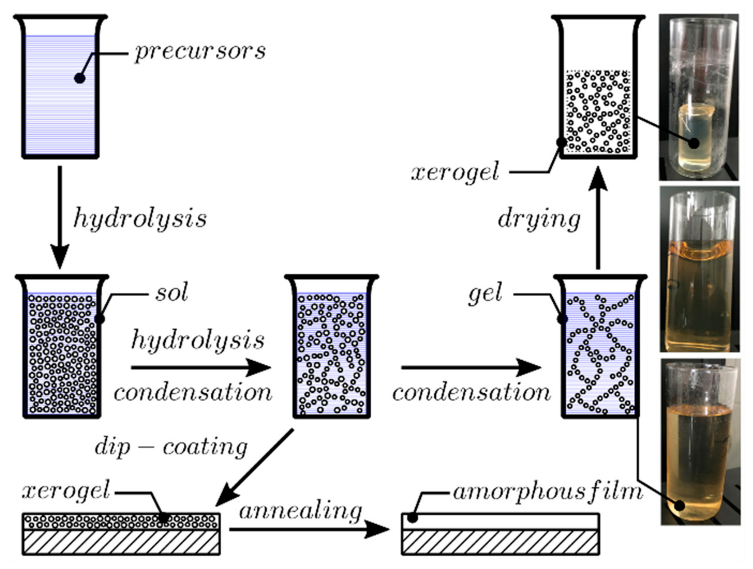
2. Advancement of Low-Cost SiO2-TiO2 Platform
The sol–gel method in combination with the dip-coating technique allows the fabrication of waveguide films in single or multiple coating regimes. This section covers the fabrication process and results of the characterization of single and double-coated SiO
2-TiO
2 waveguides on BK7 glass substrates. This process is schematically presented in
Figure 1.
Tetraethoxysilane (TEOS) and titanium (IV) ethoxide (TET) were used as the precursors to SiO2 and TiO2, respectively. These two reagents were purchased from Sigma-Aldrich. The other reagents used in sol synthesis were deionized water, anhydrous ethanol (EtOH), and hydrochloric acid (HCl). The latter was used as the catalyst for concurrently running reactions of hydrolysis and condensation. The process of preparing the SiO2-TiO2 sol was carried out in two stages. In the first stage, the hydrolysis of each precursor was carried out separately. Then, the solutions were mixed in the appropriate proportion and the process was continued. A sol fabricated this way was aged in tightly closed vessels at the temperature of 180 °C. The films were deposited on BK7 glasses slides with the dimensions of 76 × 26 × 1 mm3.
To determine the fundamental technological characteristic that shows the relationship between both thickness
d and refractive index
n of waveguide films, concerning substrate withdrawal speed from sol
v, the number of films were deposited on glass substrates, each at a different speed
v. After deposition, the films were annealed at the temperature of 500 °C for 60 min. Finally, the thickness and refractive index of those films were measured using the monochromatic, multiangle ellipsometer Sentech SE 400 adv operating at the wavelength of 632.8 nm. The resulting characteristics are presented in
Figure 2.
Both characteristics:
d(
v) and
n(
v) are very well approximated by linear functions:
d(
v) =
Ad v +
Bd and
n(
v) =
An v +
Bn. The coefficient of these functions is presented in
Table 2. Linear regression confidence bands for statistical significance level
αs = 0.05 are shown in
Figure 1.
One can see from the characteristics presented in
Figure 2 that in the presented range of
v, a maximum thickness that can be obtained in a single coating process is about 230 nm. Fabrication of thicker films is possible with the multiple coating process, which is significant in that after each coating the sample must be annealed. For this paper, we have fabricated the set of ten SiO
2-TiO
2 waveguides in the single coating process, which has enabled the determination of the characteristics presented in
Figure 2, and a few extra films in the double coating process. Apart from the monochromatic ellipsometry, waveguide films were characterized using transmission and reflection spectroscopy, atomic force microscopy (AFM), and optical transmission losses were measured using the streak method. In the paper, the results are presented for two waveguides that are marked with symbols: Wg1 and Wg2. The first one was fabricated in a single coating process for the withdrawal speed of
v = 5.4 cm/min. The second waveguide, fabricated in the double coating process, was withdrawn at speed of
v = 5.1 cm/min. The main reason for selecting only two waveguides was dictated by a willingness to compare single and double-coated waveguides for which the length of streaks of the scattered light, from which optical transmission losses were determined, are comparable and if possible. The refractive index and thickness values of the waveguide Wg2 measured using the SE400 ellipsometer and calculated from linear equations whose coefficients are given in
Table 2 are presented in
Table 3.
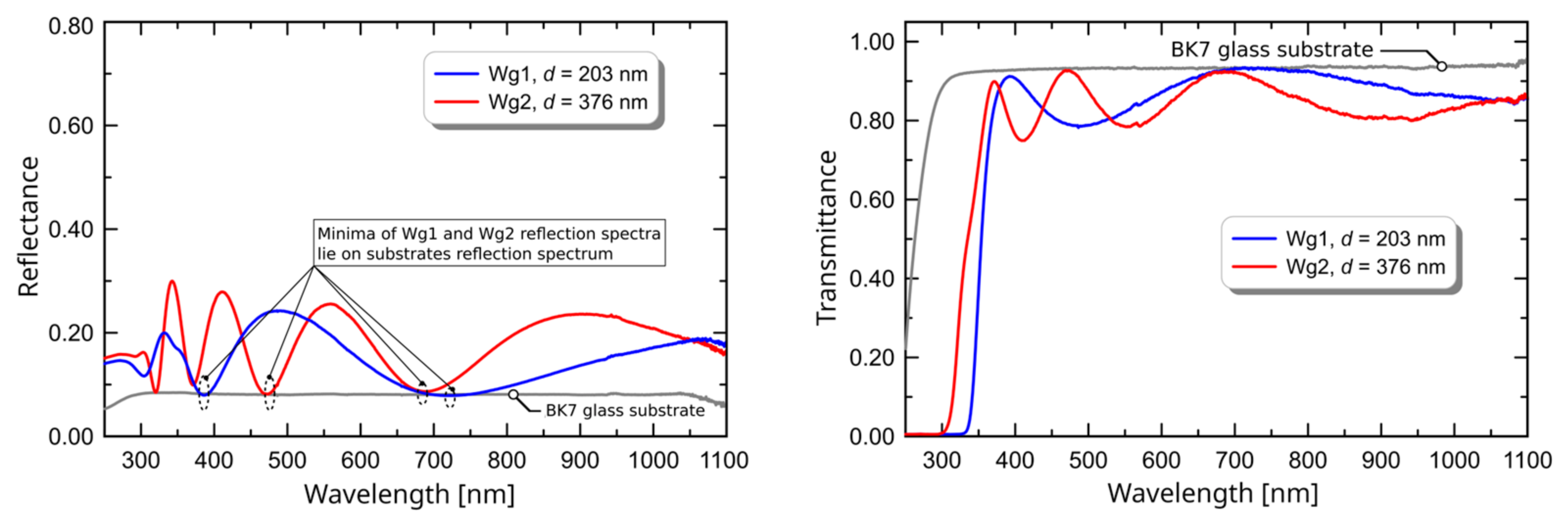
Measured values of refractive index and thickness belong to confidence intervals presented in
Figure 2. Considering the application of planar waveguides for the design of optical sensors which use the evanescent wave spectroscopy technique [
22], it is worth remembering that step-index waveguides with high refractive index contrast are the best selection for this kind of application. That is because they have maximum homogeneous or surface sensitivities [
23,
24]. Analysis of transmission of reflectance spectra allows relatively easy to conclude whether a dielectric film is homogeneous or not. However, the film must have a thickness in a range allowing for observation of interference minima and maxima. As it was shown in [
4], when maxima of transmission spectra and minima of reflectance spectra that are far from an absorption edge lay on a transmission and reflectance spectrum of the substrate, then the film is optically homogeneous—it has a uniform (step-index) distribution of refractive index in a direction perpendicular to its surface. The transmission and reflectance spectrum of Wg1 and Wg2 are presented in
Figure 3. One can observe that the maxima of transmission spectra for wavelengths greater than 450 nm lie on a spectrum of the BK7 glass substrate, as well as the minima of reflectance spectra for wavelengths greater than 400 nm. This confirms that considering the distribution of the refractive index in the direction perpendicular to the surface, investigated SiO
2-TiO
2 films are homogeneous.
The uniformity of waveguide film thickness on scales comparable to dimensions of the substrate is important for application development. The left-hand-side picture in
Figure 4 presents the waveguide film illuminated with white light. Its color, resulting from interference, is uniform, excluding areas near the edges of the sample. It bespeaks for uniformity of the waveguide film thickness. The right-hand side picture in
Figure 4 presents silica–titania waveguide film fabricated on the BK7 glass substrate in which a TM
0 mode, excited by using a prism coupler, is propagating. The experiment was conducted more than 10 years after the fabrication of that waveguide. As a result, we can witness the chemical stability of the manufactured thin films. One can observe that the streak is uniform down to the edge of the waveguide film.
The surface morphology of the silica–titania waveguide films was analyzed using the AFM method. From the central part of both investigated waveguides, rectangular samples of width 27 mm and length 20 mm were cut. The picture of the Wg2 in the AFM holder is presented in
Figure 4 (left) and the picture of the Wg2 in the prism coupler is shown in
Figure 4 (right).
Measurements were carried out using a system N_TEGRA Spectra (NT-MDT). The HA_NC (NT-MDT) silicon cantilever operated in semi-contact mode at the frequency of 220.07 kHz. The nominal curvature radius of a tip is 10 nm. Images were obtained from scans having areas of size 5 × 5 μm
2. For each sample, three scans were performed at different spots. The NOVA 1.0.26.1644 (NT-MTD) software was applied to correct the tilt of the sample and calculate the average surface roughness σ. The surface topology of Wg1 and Wg2 are shown in
Figure 5 and
Figure 6, respectively.
Fabrication of waveguide films having as small as possible surface roughness is particularly desired if those films are to have low transmission optical losses. That is because the scattering of a light wave guided in a waveguide is the main source of optical losses if material absorption is negligible. That last condition is fulfilled for silica–titania SiO
2-TiO
2. According to the model elaborated by Lacey and Payen [
25], optical losses are linearly increasing with the squared surface roughness σ on both waveguide film interfaces to a substrate and a cover. The roughness of the substrate is generally higher and depends on the quality of glass substrates. The roughness of the interface to cover depends mainly on the quality of the sol. The roughness of SiO
2-TiO
2 films is very low. The average values of σ and their maximum absolute deviations determined from three points on the Wg1 and Wg2 are σ
Wg1 = 0.58 ± 0.29 [nm] and σ
Wg2 = 0.63 ± 0.33 [nm]. One can see that the average surface roughness of the film fabricated in a double coating process is only slightly higher. To validate whether the surface roughness is increasing because of repetition of the coating process, or the result reported here is a mere accident, requires further systematic study.
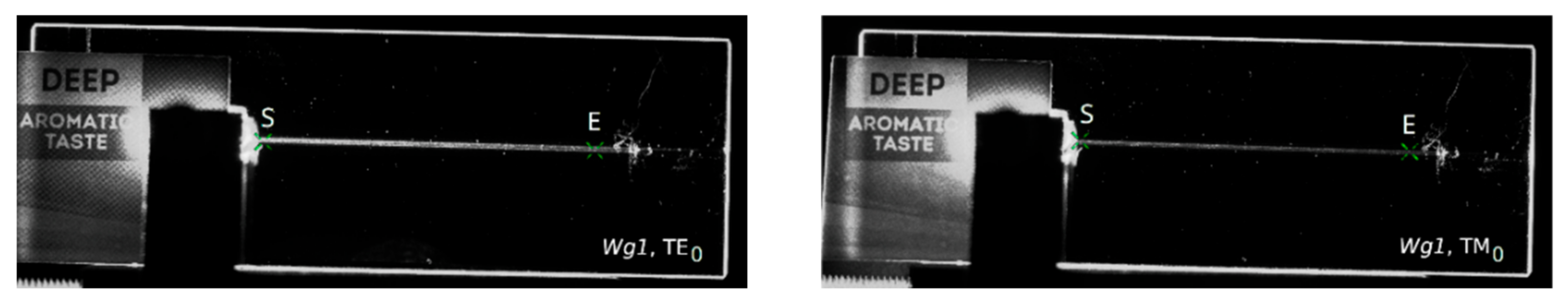
Finally, fabricated waveguides were verified by coupling light into them using a prism coupler and observing streaks of scattered light accompanying the propagation of fundamental waveguide modes: TE
0 and TM
0. The picture of the Wg
2 in the prism coupler holder is presented on the right in
Figure 4. A laser diode operating at the wavelength
λ = 677 nm was used as a light source. Optical transmission losses of guided modes can be determined assuming that the distribution of light intensity in such a streak is directly proportional to the distribution of light intensity of the guided mode. Assuming that the light intensity is exponentially decaying
, the attenuation coefficient, which is equal to
, can be calculated by fitting a linear function to the distribution of the natural logarithm of normalized light intensity
In. The latter was obtained for each linear scan selected from captured images of light streaks by dividing intensity values by the maximum value in the given streak. The images are shown in
Figure 7 and
Figure 8. The lines’ endpoints (S and E) are marked by a green cross. The linearized distributions of normalized light intensity are presented in
Figure 9 and
Figure 10. Streaks of scattered light were registered using a scientific grade, monochromatic camera Thorlabs 1501 equipped with a lens MVL35M23—35 mm EFL. The camera produces grayscale pictures with a resolution of 1392 × 1040 pixels and 14-bit depth. The light intensity
I expressed in arbitrary units changes from 0 to 16,383.
Determined values of optical transmission losses α and their deviations uα for both investigated waveguides and both polarizations are presented in
Table 4. One can observe that optical losses for the Wg2 waveguide are smaller. That is because this waveguide is thicker than Wg1. Fundamental modes are better confined to the Wg2. The results show the density of optical power on the interface to the cover is smaller and in consequence, optical transmission losses are smaller. This experiment proves that fabricated SiO
2-TiO
2 waveguide films, both single-coated and double-coated, have very good transmission properties.
3. Device Design and Numerical Model
In this section, the potential filtering and sensing applications based on the SiO
2-TiO
2 platform have been numerically demonstrated.
Figure 11a,b depict the SWG waveguide NIR-filter and SWG waveguide FP-sensor architecture, respectively. SWG waveguides have enticed a significant amount of interest as they allow for customized EM-wave propagation by adjusting period (
ᴧ), which is the sum of
L and
d, where
L is the length of the waveguide segment and d is the distance between two segments. The total length of the waveguide is considered as ((
ᴧ ×
N) −
d), where
N is the total number of periods as shown in
Figure 11. The height and width of the waveguide segments are represented as
H and
W, respectively. The refractive index of the silica substrate is taken at 1.45 for the operational wavelength of 980 nm. Whereas, the refractive index of the SiO
2-TiO
2 thin film is selected from the real part of the effective refractive index, which is dependent on the dimension of the waveguide core. The E-field distribution in the SWG waveguide at different points along the propagation direction is shown in
Figure 11c.
The SWG waveguides were modeled using a 2D finite element method (FEM) based on COMSOL Multiphysics 5.5. As a physics interface, the EM-wave frequency domain was utilized. The FEM reduced large elements into smaller components identified as finite elements. This may have been accomplished by performing a space discretization in the space dimensions, which was carried out by generating an object mesh. The detailed meshing was determined by the accuracy of the solution and the computer’s processing power. For the whole waveguide model, we utilized a mesh size of λ/30. Based on our system’s processing speed, this meshing produced accurate simulation results. A domain with an open computation domain was used for wave propagation systems because it allows the EM-wave to flow without back reflections. The open geometry was allotted by using the scattering boundary condition (SBC) at the simulation windows outside borders. At the waveguide’s input port, an x-oriented plane wave was excited. Furthermore, the “parametric sweep” function is utilized to simulate various geometric aspects of the waveguide concerning a certain wavelength range.
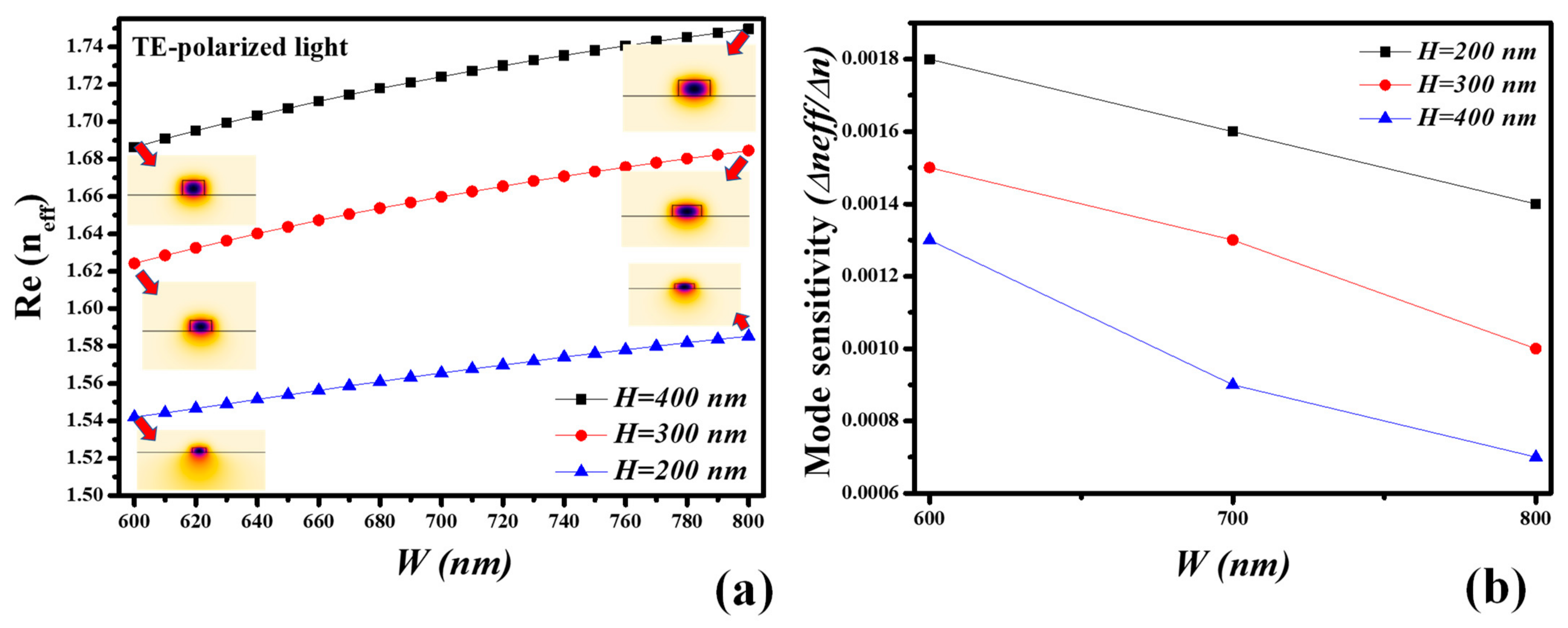
The real part of the effective refractive index (n
eff) of the transverse electric (TE) mode is intended for the operation wavelength of 980 nm by varying the dimensions of the ridge waveguide. This examination is imperative to find the waveguide geometry for the best sensing performance. The height (
H) of the SiO
2-TiO
2 waveguide core is considered as 200 nm, 300 nm, and 400 nm which is practically realizable via single and multiple dip-coating methods. The width (
W) of the waveguide core is varied between 600 nm and 800 nm. From
Figure 12a, it can be seen that the Re (n
eff) surges as the
W and
H of the waveguide core increase which indicates the better mode confinement in the core. Consequently, the contact of the evanescent field with the ambient medium is less which results in low sensitivity. Therefore, we must choose the waveguide core dimensions near the cut-off wavelength where the maximum evanescent field is present. In
Figure 12b, the mode sensitivity analysis is executed by changing the ambient refractive index (ARI) from 1.33 to 1.34, resulting in the shift in the effective index of the TE-mode. The sensitivity is calculated as ∆
neff/∆
n. The mode sensitivity of the waveguide core with smaller dimensions is higher than the sensitivity offered by bigger waveguide cores. This indicates the maximum sensitivity of 0.0018 ∆
neff/∆
n is attained at the waveguide core of
H = 200 nm and
W = 600 nm.
4. NIR Filtering Application
The optical band-rejection filters are implemented using a variety of methods. A few of these are described here, for example: In [
26], an optical band-rejection filter was established on a multistage μ-ring add-drop filter with an extinction ratio (
ER) > 50 dB, and bandwidth (BW) of 32 GHz has been proposed. An experimental demonstration of a wide optical band-rejection filter with a modest footprint established on two parallel rows of an anti-symmetric one-dimensional Photonic crystal with a defect in a multimode waveguide is presented in [
27]. It has an
ER of 25 dB and a stopband of 200 nm. Another method for constructing an optical band-rejection filter is to use a cladding modulated anti-symmetric long-period grating in a two-mode silicon waveguide. It has a BW of 4.3 nm and an
ER of more than 15 dB by adopting a 1040 μm long cladding modulated long-period grating [
28]. There are other efforts to develop broadband adjustable optical band-rejection filters established on a multimode 1D Photonic crystal waveguide with an 84 nm BW. The device has a 40 × 1 m
2 footprint [
29]. The device performance of the SWG waveguide NIR filter is discussed in terms of
ER and BW.
ER is calculated as
where
Pout and
Pin are the output and input power, respectively. Additionally, the 3 dB BW is obtained from the transmission spectrum where the power level of the signal declines by 3 dB from its maximum value.
The transmission spectrum of the SWG waveguide NIR-filter versus the
DC is plotted in
Figure 13a. The geometric parameters such as
W,
H,
L, and
N are fixed at 800 nm, 400 nm, 400 nm, and 10, respectively, as the device is designed for filtering applications. Therefore, the choice of
W = 800 nm and
H = 400 nm is based on our previous analysis where we determined the low mode sensitivity of the structure. Whereas, the
DC varies between 66.7% and 80%, resulting in the enhancement in the
ER and the 3-dB BW of the filter. Thus, it is determined that the stopband region can be adjusted by choosing the proper
DC. Furthermore, the influence of
N on the transmission spectrum is analyzed in
Figure 13b.
N plays a momentous role in augmenting the
ER of the stopband region without altering the BW and the region of the stopband. The summary of the
ER and 3 dB BW dependent on the
DC and
N is presented in
Table 5. The E-field distribution of the SWG waveguide filter in the stopband (indicated by red dots in
Figure 13b) and above the λ
Bragg (indicated by red dots in
Figure 13b) is presented in
Figure 13c (left) and
Figure 13c (right), respectively.
DC plays an imperative role in enhancing the
ER and 3dB-BW of the SWG waveguide stopband filter. From
Table 5, it can be seen that, as the
DC varies from 80% to 66.7%, the
ER increases from ~19 dB to ~41.9 dB.
ER can also be modified by adjusting the
N at a constant
DC. The 3 dB BW of the filter upsurges from 79 nm to 110 nm as the
DC changes from 80% to 66.7%.
5. Sensing Application
A cavity of size 2
L is inserted in the center of the SWG waveguide to create an FP-sensor structure as shown in
Figure 11b. The geometry of the SWG waveguide-FP structure needs to be optimized for the best sensing performance. The
DC,
N, and
W are important parameters that should be carefully handled while designing such devices. At first, the FP-wavelength occurring in the stopband region is determined concerning the
DC of the device structure which is varied between 66.7% and 80%, while keeping
W,
H,
L, and
N constant at 800 nm, 400 nm, 400 nm, and 10, respectively. The surrounding medium is air (
n = 1.0). As shown in
Figure 14a, the FP-wavelength shows a blueshift as the
DC increases from 66.7% to 80%, which signifies that the desired spectral properties can be obtained by varying the
DC of the device.
In the second step, the influence of
N on the spectral properties of the SWG waveguide-FP structure is determined as shown in
Figure 14b. The remaining geometric parameters such as
W,
H, and
DC are fixed at 800 nm, 400 nm, and 80%, respectively. It can be seen that, as
N increases from 6 to 14, the
ER of the stopband significantly increases from ~17 dB to ~30 dB with a reduction in the full width at half maximum (FWHM) of the FP-wavelength. Therefore, a precise selection of
N is important, however, a bigger
N can lead to a bigger device footprint.
For sensing applications, a large overlap of an evanescent field with the ambient medium is required for enhanced sensing devices. Therefore,
W plays an important role in increasing the sensitivity and if the device is designed close to the cut-off dimensions of the waveguide, then maximum sensitivity can be obtained. The transmission spectrum of the SWG waveguide-FP structure is plotted for
W varying in the range of 600 nm and 800 nm, as shown in
Figure 14c. The remaining geometric parameters such as
H,
DC, and
N are fixed at 400 nm, 80%, and 10, respectively. The FP-wavelength performs a blueshift as
W decreases from 800 nm to 600 nm. From
Figure 14a,c, we can see that
DC and
W have direct control over tuning the FP-wavelength.
The E-field distribution in the SWG waveguide NIR-filter structure at Bragg wavelength (λ = 748 nm), FP wavelength (λ = 777 nm), and above Bragg wavelength (λ = 816 nm) is shown in
Figure 15 (left),
Figure 15 (middle), and
Figure 15 (right), respectively. This indicates the behavior of EM wave in the stopband, FP-cavity, and the passband.
To demonstrate the sensing performance of the FP-structure, the wavelength interrogation method has been used. Sensitivity (
S) is the ratio between the change in the FP-wavelength and the change in the ARI, which is expressed as:
where ∆
λ and ∆
n are the change in FP-wavelength and the change in ARI, respectively. The ambient index varies between 1.33 and 1.37 with a step size of 0.005. The FP-wavelength and sensitivity of the device having different dimensions concerning the changing ARI are shown in
Figure 16a,b, respectively. The
S of the FP-structure varies between 80 nm/RIU and 120 nm/RIU at
H = 400 nm by reducing the
W from 800 nm to 600 nm. Additionally, this sensitivity can be further enhanced to 20–30% by reducing
H from 400 nm to 200 nm. The sensitivity characteristics of the SWG waveguide FP-structure are summarized in
Table 6. In [
30], Fard et al. used 90 nm SOI strip waveguide height to enhance bulk sensitivity.


 ,
, 


