


Nanomaterials 2026, 16(6), 351; https://doi.org/10.3390/nano16060351 - 12 Mar 2026
Viewed by 721
Abstract
►
Show Figures
Metasurface is a kind of artificial structure which can efficiently control the amplitude, phase, frequency, and polarization of the light field. Metasurface polarization holographic encryption is a holographic encryption technology with the polarization state as a key, which has been widely concerned in
[...] Read more.
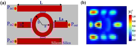
Metasurface is a kind of artificial structure which can efficiently control the amplitude, phase, frequency, and polarization of the light field. Metasurface polarization holographic encryption is a holographic encryption technology with the polarization state as a key, which has been widely concerned in recent years with advantages such as sub-wavelength pixels, precision adjustment, and high security factor. In this paper, the design and optimization of the unit structure of metasurface have been carried out, and the clear double-channel holographic image reproduction and good encryption effects have been realized afterwards. The results show that the relatively good polarization holographic encryption can be achieved by employing the designed Si nanorods with the length of 148 nm and width of 55 nm, respectively, which have been beforehand grown on SiO2 substrates. Note that the periodic angle deflection around the Z axis was adopted by using the dual-channel optical rotation incidence with the wavelength of 632.8 nm. It has been theoretically demonstrated that information transmittance loss should be less and the image restoration effect should be satisfactory. A novel encryption method has also been proposed for the optical information processing and optical encryption, and the huge application potential of our theme has been revealed as the next-generation optical control platform in the near future.
Full article

Figure 1


