1. Introduction
Electromagnetic interference (EMI) has become a critical limitation in modern high-speed digital systems, particularly as CMOS technologies continue to scale toward nanoscale dimensions. The reduction in supply voltage, combined with increased circuit density and reduced noise margins, has significantly increased susceptibility to external disturbances. Under such conditions, even low-power RF interference can induce measurable perturbations in signal amplitude and degrade system performance.
Eye diagrams are widely used as a compact and intuitive tool for evaluating signal integrity in digital systems. By superimposing multiple bit periods, eye diagrams provide direct insight into noise amplitude, timing jitter, and inter-symbol interference, enabling rapid assessment of signal quality [
1]. Early efforts to extract quantitative information from eye diagrams included image-based and statistical processing approaches [
2]. In addition, circuit-level studies have examined the effect of deterministic noise sources on jitter behavior in CMOS inverters, highlighting the sensitivity of digital waveforms to externally induced disturbances [
3]. Fast computational approaches for eye diagram analysis in CMOS circuits have also been reported for high-speed applications [
4]. More general discussions of eye diagram interpretation have further established the eye diagram as a standard diagnostic tool in high-speed electronics [
5].
Analytical and statistical techniques for eye diagram evaluation have been widely studied in optical and electrical signaling systems. Accurate calculation of eye diagrams and bit error rates has been reported using linearization-based methods [
6], while experimental eye diagram and bit error rate (BER) measurement techniques based on asynchronous sampling have also been demonstrated [
7]. More recently, transmitter and dispersion eye closure metrics have been investigated in PAM4 waveform analysis [
8], and robust algorithmic approaches for eye diagram analysis have been developed for measurement applications [
9]. Polynomial-based estimation techniques have also been proposed to predict eye diagram behavior for pseudo-random bit sequence (PRBS)- based bit streams in high-speed signaling environments [
10]. In parallel, phase-noise and timing-fluctuation modeling studies have provided a broader foundation for understanding waveform uncertainty in electronic circuits [
11].
Despite these advances, most existing studies are either simulation-driven or focused on channel-induced impairments rather than experimentally controlled EMI coupling at the circuit level. In practical systems, EMI coupling through the power distribution network represents a major pathway for signal degradation, where RF disturbances injected at the supply node can propagate through the circuit and directly influence output signal amplitude, particularly in CMOS logic stages. However, there is a lack of systematic experimental characterization on how controlled levels of RF injection affect the signal quality as measured by eye diagrams. The mechanism by which EMI coupling closes the eye diagram remains unclear, with debate over whether amplitude variation or time jitter is the dominant effect, and existing literature does not provide a clear answer. Several studies have employed Direct Power Injection (DPI) and related RF-injection techniques to evaluate the electromagnetic susceptibility of integrated circuits [
12]. These approaches are primarily intended for immunity characterization and compliance assessment. In contrast, the present work focuses on the physical manifestation of EMI at the waveform level through eye-diagram analysis.
Our previous work has investigated EMI effects in electronic systems from both system-level [
13] and device-level [
14] perspectives. These studies demonstrate the strong coupling between externally injected RF interference and circuit behavior, motivating the need for a direct investigation of EMI-induced signal degradation at the waveform level using eye diagram analysis.
Motivated by these considerations, this work experimentally characterizes the impact of RF interference on digital signal integrity using eye diagram analysis. CMOS inverter test structures fabricated in 65 nm, 130 nm, and 180 nm technologies are employed as a controlled platform for studying EMI-induced degradation. The CMOS inverter test chips were designed at the University of New Mexico and were sent to the MOSIS Very Large Scale Integration Circuit Fabrication at the University of Southern California for fabrication. These technology nodes span multiple generations of CMOS scaling and provide different supply voltages, device dimensions, parasitic characteristics, and noise margins, enabling comparison of EMI susceptibility across distinct device generations. In addition, mature CMOS nodes remain relevant in mixed-signal, RF, automotive, aerospace, and radiation-tolerant electronic systems, where robustness and long-term reliability are critical.
RF interference is injected at the supply node, and the resulting signal behavior is analyzed using time-domain measurements and corresponding eye diagrams. The primary objective is to identify the dominant degradation mechanism and establish a quantitative relationship between interference amplitude and signal-integrity metrics.
The main contributions of this work are summarized as follows:
A systematic experimental characterization of EMI-induced signal degradation under controlled RF injection at the circuit level
Identification of amplitude modulation in the logic-high state as the dominant mechanism responsible for eye diagram degradation
Development of a compact analytical model relating eye height reduction to the amplitude of injected RF interference
Experimental validation of the proposed model across multiple CMOS technology nodes (65 nm, 130 nm, and 180 nm).
This framework provides a practical basis for predicting EMI susceptibility and guiding the design of robust high-speed digital systems.
2. Experimental Setup and Results
The experimental investigation was conducted using CMOS inverter test structures fabricated in TSMC (Taiwan Semiconductor Manufacturing Company, TSMC, Phoenix, AZ, USA) 65 nm, 130 nm, and 180 nm technology nodes. A 10x CMOS inverter (10×INV) was used as the device under test (DUT), providing sufficient signal propagation depth to amplify the impact of small perturbations. This structure was selected due to its fundamental role in digital systems and its sensitivity to supply-induced disturbances, making it well suited for evaluating EMI-induced signal degradation.
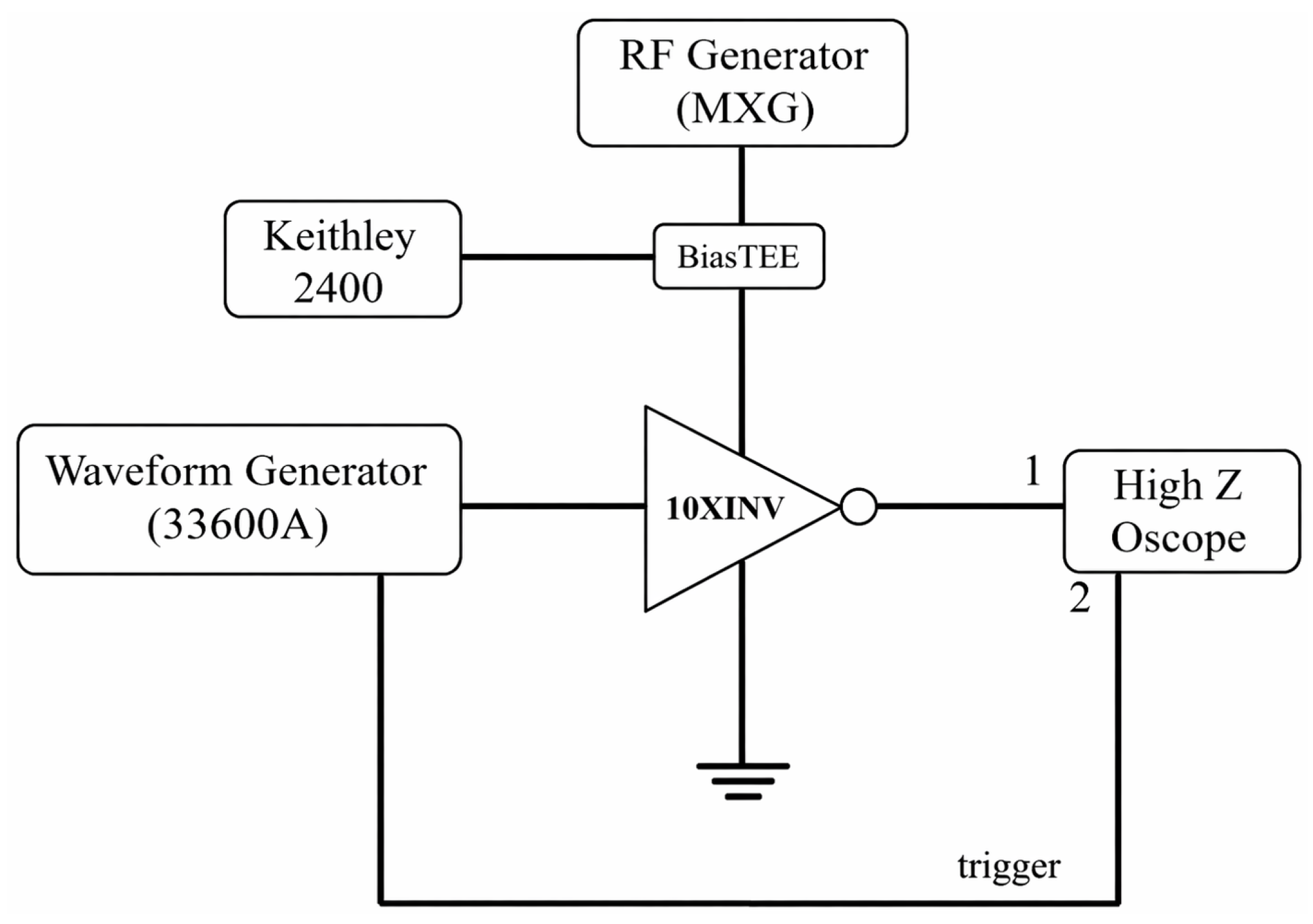
The measurement setup is illustrated in
Figure 1. A pseudo-random bit sequence (PRBS) was generated using an arbitrary waveform generator and applied to the input of the inverter as a non-return-to-zero (NRZ) signal. The bit rate was set to 4 Mbps to ensure stable time-domain observation while maintaining sufficient temporal resolution for eye diagram formation. The signal amplitude was matched to the nominal supply voltage of each technology node.
Controlled RF interference was injected at the node using an RF signal generator (Keysight Technologies, Santa Rosa, CA, USA). A bias-tee was employed to combine the RF signal with the DC supply voltage provided by a source meter, ensuring simultaneous biasing and perturbation of the DUT. The RF carrier frequency was fixed at approximately 10 MHz, and the injection power () was varied from dBm to dBm. The current results reflect supply-coupled EMI only, and the relative dominance of this coupling path in realistic environments with multiple simultaneous coupling mechanisms remains to be verified. All measurements were performed under identical room-temperature laboratory conditions. For each technology node, a baseline waveform was first recorded without RF injection, followed by measurements at each RF power level while maintaining the same supply voltage, input waveform, probing configuration, and acquisition settings. The output waveform was captured using a high-impedance oscilloscope with sufficient bandwidth to preserve waveform fidelity.
The baseline measurements established reference eye diagrams for each technology node. Under these conditions, the eye diagrams exhibited wide openings with clearly separated logic levels, indicating minimal amplitude noise and negligible distortion. As RF injection was introduced, progressive degradation in the eye diagram was observed.
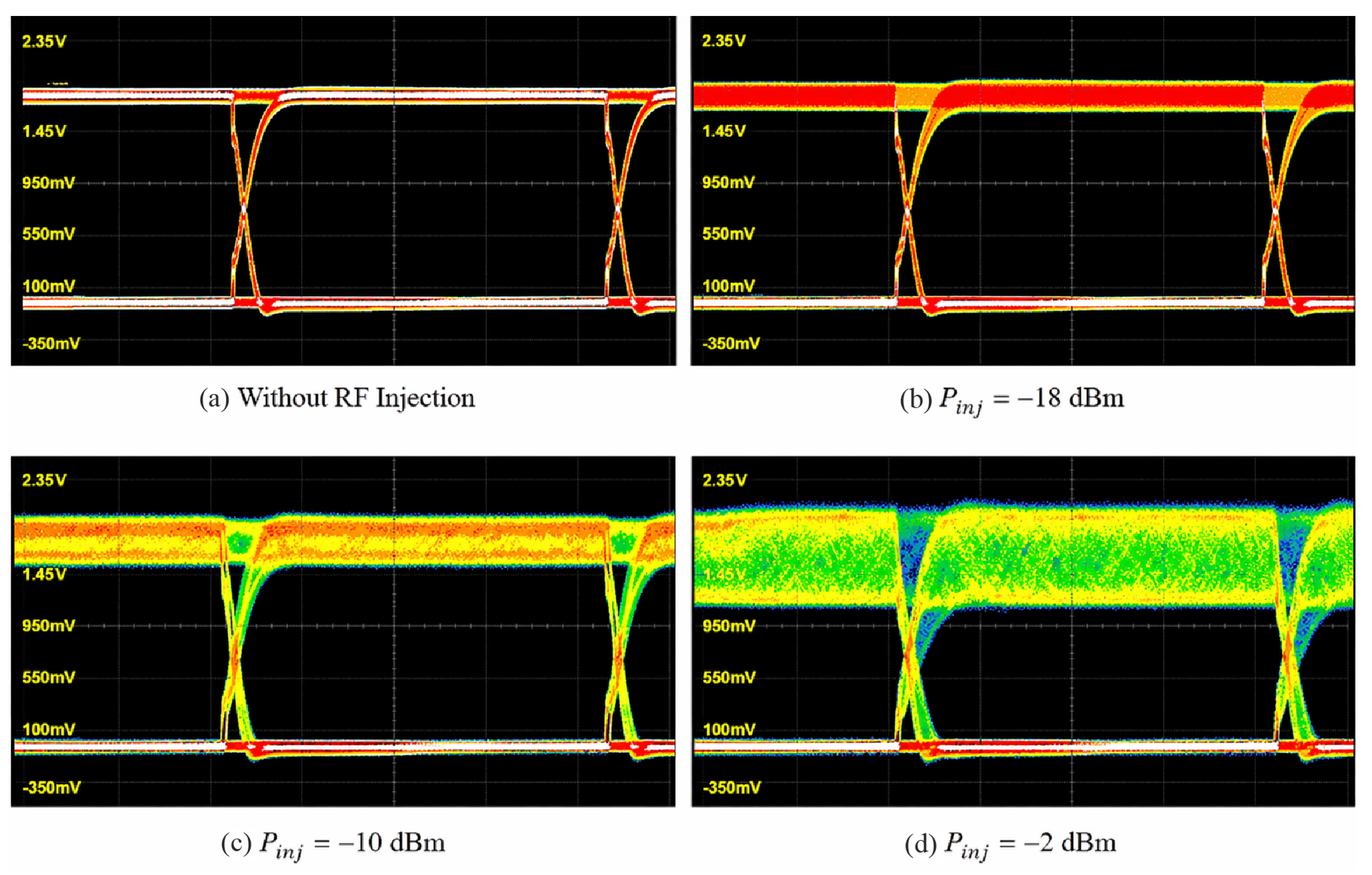
Figure 2 shows representative eye diagrams for increasing levels of RF injection power. At low injection levels (e.g.,
dBm), small amplitude fluctuations begin to appear in the logic-high region. As the injection power increases, these fluctuations become more pronounced, leading to a widening of the distribution associated with the logical ‘1’ level. At higher injection levels (e.g.,
dBm), the spread becomes sufficiently large that the eye opening is significantly reduced, indicating degraded signal integrity.
A key observation is that the degradation is strongly asymmetric. The logic-high level exhibits significant amplitude variation, whereas the logic-low level remains relatively stable. This behavior can be explained by considering the operating states of the CMOS inverter. During the logic-high output state, the PMOS transistor actively drives the output node, making it susceptible to perturbations coupled through the supply voltage. In contrast, during the logic-low state, the NMOS transistor provides a low-impedance path to ground, effectively suppressing the influence of RF disturbances. As a result, EMI-induced degradation primarily manifests as amplitude modulation in the logic-high state.
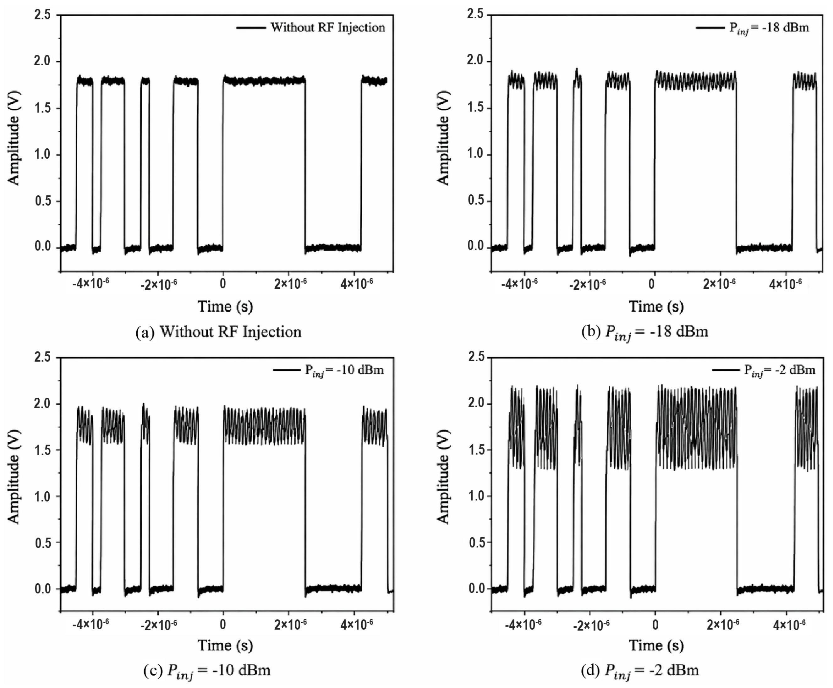
This effect is further illustrated in the time-domain waveforms shown in
Figure 3. With increasing RF injection power, the output signal exhibits clear amplitude modulation, primarily at the logic-high level, while the logic-low level remains comparatively less affected. Because the RF interference is not synchronized with the input data pattern, the high-level voltage varies from bit to bit when observed over multiple bit periods. When these waveforms are folded over repeated unit intervals to form the eye diagram, this variation appears as increased vertical spreading of the traces, reducing the eye height and contributing to eye closure.
To quantify the degradation, the eye height was extracted from the measured eye diagrams for each RF injection level. The eye height was defined as the vertical separation between the mean logic-high and logic-low levels, accounting for the spread of the voltage distribution.
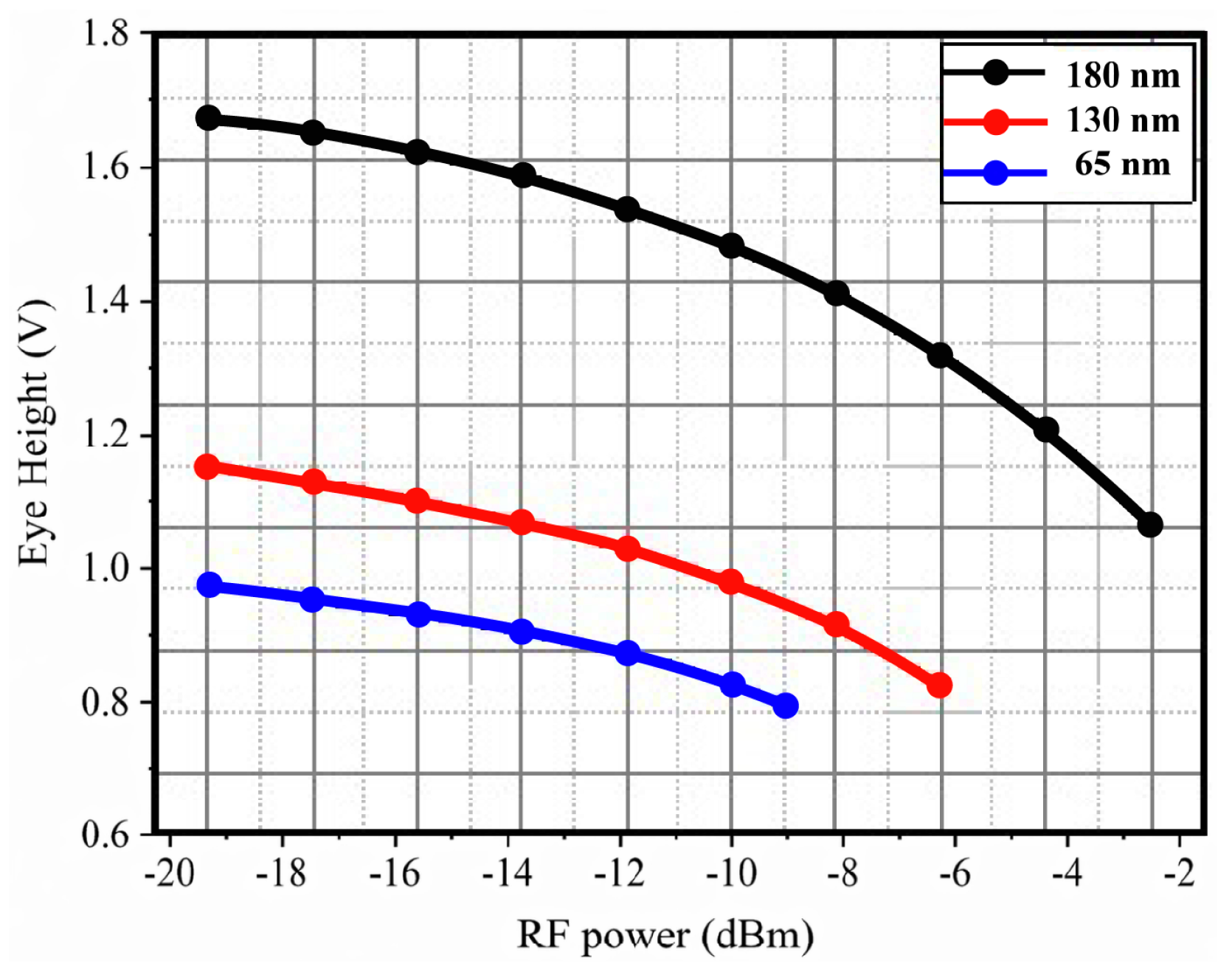
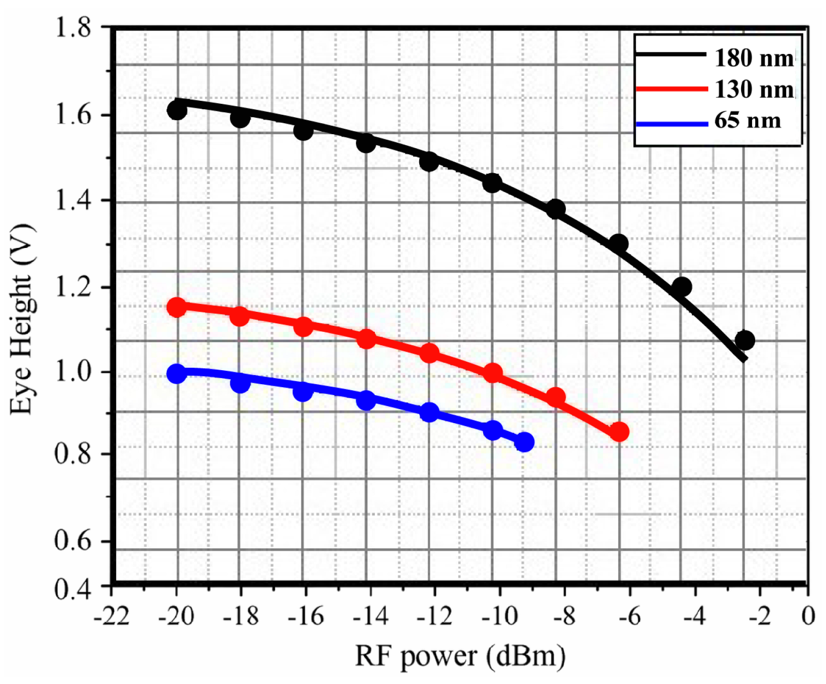
Figure 4 shows the measured eye height as a function of RF injection power for the three technology nodes. A monotonic decrease in eye height is observed as the injection power increases, indicating progressive loss of signal margin.
Among the tested devices, the 180 nm technology exhibits the most pronounced degradation, followed by the 130 nm and 65 nm nodes. This trend suggests that larger-geometry technologies are more susceptible to externally injected disturbances, likely due to increased parasitic capacitances and reduced effectiveness of intrinsic noise suppression mechanisms. Although this explanation is qualitative, it is consistent with the observed experimental behavior.
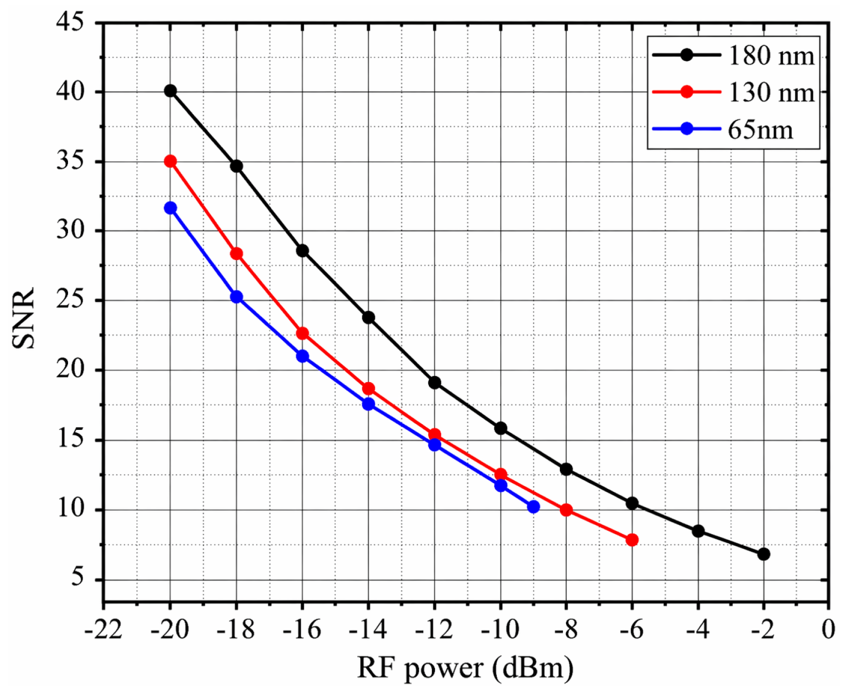
In addition to eye height, the signal-to-noise ratio (SNR) was evaluated as a complementary metric.
Figure 5 shows the measured SNR as a function of RF injection power. A consistent reduction in SNR is observed with increasing interference level, confirming that the injected RF signal introduces significant amplitude noise into the system. The relationship between signal degradation and SNR is consistent with established signal-quality metrics commonly used in communication-system analysis [
15]. The trends observed in SNR closely follow those of the eye height, reinforcing the interpretation that amplitude fluctuations are the dominant degradation mechanism.
These results demonstrate that EMI-induced signal degradation in CMOS inverter is primarily governed by amplitude modulation of the logic-high level. The monotonic reduction in both eye height and SNR with increasing RF injection power provides a clear and consistent characterization of this behavior across multiple technology nodes. These observations form the basis for the analytical model developed in the following section and are consistent with established signal-integrity behavior in high-speed digital systems [
16].
3. Predictive Model for Eye Diagram Under EMI and Model Validation
To complement the experimental observations, a compact analytical model is developed to predict eye diagram degradation in the presence of EMI. While prior studies have investigated eye diagram behavior using analytical, statistical, and computational approaches [
6,
8,
9,
10,
17], these efforts are primarily focused on channel-induced impairments or simulation-based frameworks. In contrast, the present work aims to establish a direct relationship between externally injected RF interference and measurable signal degradation at the circuit level.
The injected EMI is modeled as a sinusoidal perturbation superimposed on the nominal digital signal. This representation reflects a practical scenario in which the RF interference is not synchronized with the digital switching activity. The injected signal can therefore be expressed as
where
is the amplitude of the injected RF signal and
f is its frequency.
Since the RF perturbation is asynchronous with respect to the digital signal, its instantaneous effect varies across different bit periods. When observed over many cycles, this deterministic sinusoidal disturbance manifests as an effective amplitude fluctuation in the logic-high level. This behavior justifies a statistical characterization of the voltage variation associated with the logical ‘1’ state.
The CMOS inverter is primarily sensitive to supply-induced perturbations during the logic-high output state, where the PMOS device actively drives the output node. Therefore, the analysis is restricted to the voltage distribution corresponding to the logic-high level. The effective amplitude variation introduced by the RF signal can be approximated by an equivalent peak-to-peak perturbation , which accounts for the coupling of the injected RF signal into the output waveform.
Assuming a sinusoidal perturbation, the standard deviation of the induced amplitude variation can be approximated as
where
represents the effective standard deviation of the logic-high voltage distribution. The factor
arises from the relationship between the peak-to-peak voltage and the standard deviation of a sinusoidal signal. For a sinusoid with peak amplitude
A, the standard deviation is
, while the effective peak-to-peak voltage is
. Substituting
yields Equation (
2).
The effective perturbation
is related to the injected RF signal through a technology-dependent scaling factor
n, such that
where
is the peak-to-peak amplitude of the injected RF signal. The parameter
n is interpreted as an effective supply-to-output coupling coefficient that relates the injected RF disturbance at the supply node to the resulting voltage fluctuation observed at the inverter output. It is not a fundamental transistor parameter; rather, it compactly captures the combined effects of supply sensitivity, device gain, parasitic coupling, and technology-dependent circuit characteristics. In this work,
n is extracted from measured data, but in principle it could also be obtained from an independent small-signal supply-to-output transfer measurement. The factor
defines the statistical eye-closure criterion, whereas
n describes the physical coupling from the RF-injected supply disturbance to the output-voltage fluctuation; therefore, the two quantities serve different roles in the model.
Substituting into the expression for
, the standard deviation can be written as
The eye height
h is defined as the vertical separation between the logical ‘1’ and ‘0’ levels, accounting for voltage variations. Since the logic-low level is largely unaffected by RF injection (i.e.,
), the eye height can be expressed as
where
and
represent the nominal logic-high and logic-low voltages, respectively.
The factor
was selected to provide a conservative estimate of eye closure. Under a Gaussian-equivalent approximation, approximately 99.7% of voltage excursions are contained within
, whereas a
criterion would capture only approximately 95% of the distribution. Therefore, the use of
provides a more robust representation of worst-case signal degradation and is commonly adopted in statistical eye-diagram analysis and margin evaluation [
9,
16].
Substituting the expression for
, the final form of the predictive model is obtained as
This expression establishes a direct relationship between eye-height degradation and the amplitude of the injected RF interference. It indicates that, under the measurement conditions considered in this work, signal degradation is primarily governed by amplitude fluctuations in the logic-high state, which reduce the effective noise margin of the digital signal. The model, therefore, focuses on vertical eye closure caused by RF-induced amplitude modulation. Although limited horizontal spreading is visible in the measured waveforms, timing jitter is not included in the first-order analytical formulation. At higher data rates, higher RF interference frequencies, or under coupling mechanisms that directly perturb the input timing or switching threshold, timing jitter may become more significant and should be incorporated into an extended model.
The 4 Mbps bit rate used in this study was selected to isolate the fundamental supply-coupled EMI mechanism under controlled measurement conditions. At substantially higher data rates, the interaction between RF interference and digital switching may change, especially when the RF frequency becomes comparable to the bit rate or to the spectral content of the signal transitions. Lower RF frequencies are expected to produce slower amplitude modulation of the logic-high level, whereas higher RF frequencies may introduce additional effects, including increased timing jitter, transition distortion, and frequency-dependent coupling through parasitic capacitances. Therefore, extension of the present model to Gbps-rate systems requires further characterization over a wider range of data rates and RF interference frequencies.
The extracted values of the scaling parameter
n, the corresponding voltage swing
, and the average absolute prediction error for each technology node are summarized in
Table 1. The parameter
n reflects the sensitivity of each technology to supply-coupled EMI. Although the 180 nm technology exhibits a lower value of
n, it shows greater overall degradation due to its larger nominal voltage swing and increased susceptibility to amplitude perturbations, highlighting the combined influence of device characteristics and signal levels.
The predicted eye height as a function of RF injection power is evaluated and compared with experimental measurements in
Figure 6. The model captures the observed monotonic reduction in eye height with increasing RF power and shows strong agreement with measured data across all technology nodes. Both the trend and magnitude of degradation are accurately reproduced.
To quantify the model agreement, the prediction error was evaluated by comparing the analytically predicted eye height with the measured eye height at each RF injection level. The average absolute percentage error was calculated as
where
and
are the measured and predicted eye heights at the
ith RF injection level, respectively, and
N is the total number of measurement points.
The average absolute prediction error remains below 2% for all investigated technology nodes, providing quantitative evidence of the strong agreement between the analytical model and the experimental measurements. This agreement validates the underlying assumption that EMI-induced signal degradation is dominated by amplitude modulation of the logic-high level.
The proposed model provides a simple yet physically meaningful framework for predicting eye diagram degradation under EMI conditions. It enables rapid estimation of signal-integrity degradation based on measurable RF interference parameters, without requiring extensive numerical simulations or complex statistical analysis. This capability is particularly useful for EMC-aware design, signal-integrity assessment, reliability evaluation, and early-stage EMI susceptibility screening of high-speed digital systems.
4. Conclusions
This study presents an experimental and analytical investigation of electromagnetic interference (EMI) effects on eye diagram characteristics in CMOS inverter-based digital systems. Controlled RF injection at the supply node enabled systematic characterization of signal degradation across 65 nm, 130 nm, and 180 nm technology nodes.
Experimental results indicate that EMI-induced degradation is primarily governed by amplitude modulation of the logic-high level, whereas the logic-low level remains largely unaffected. This asymmetric behavior leads to a progressive reduction in eye height and signal-to-noise ratio (SNR) as RF injection power increases. Among the evaluated devices, larger-geometry technologies exhibit greater susceptibility to EMI, underscoring the influence of device characteristics on signal integrity.
A compact analytical model was developed to describe the relationship between eye-height degradation and the amplitude of the injected RF interference. The model incorporates an effective supply-to-output coupling coefficient that captures the susceptibility of the circuit to supply-coupled EMI. Comparison with experimental results showed strong agreement in both trend and magnitude across all investigated technology nodes, with an average absolute prediction error below 2%. These results confirm that the dominant degradation mechanism is accurately represented by the proposed formulation.
The proposed framework provides a practical approach for estimating EMI-induced signal degradation based on measurable interference parameters, without requiring complex simulations. These results establish eye height as a sensitive and reliable metric for evaluating EMI susceptibility in high-speed digital systems.
The present study focuses on supply-coupled EMI and a first-order amplitude-based description of eye closure. Future work will extend the approach to higher data rates, higher RF interference frequencies, additional coupling paths, and more complex digital systems. Incorporating timing jitter and multipath EMI coupling into the predictive framework will further improve its applicability to realistic high-speed electronic environments.