Article

Enhancing CMRR in Fully Differential Amplifiers via Power Supply Bootstrapping

by
Enrique M. Spinelli
*,
Valentín A. Catacora
,
Federico N. Guerrero
and
Marcelo A. Haberman
Instituto de Investigaciones en Electrónica, Control y Procesamiento de Señales LEICI (Universidad Nacional de La Plata UNLP, Comisión Nacional de Investigaciones Científicas y Técnicas CONICET), 48 y 116, La Plata B1900, Buenos Aires, Argentina
*
Author to whom correspondence should be addressed.
Chips 2025, 4(2), 27; https://doi.org/10.3390/chips4020027
Submission received: 7 May 2025 / Revised: 26 May 2025 / Accepted: 30 May 2025 / Published: 3 June 2025
(This article belongs to the Special Issue IC Design Techniques for Power/Energy-Constrained Applications)

Abstract

:
Fully differential amplifier circuits are well suited for instrumentation front ends and signal-conditioning applications. They offer high common-mode rejection ratios (CMRRs) regardless of the passive component tolerances but remain sensitive to imbalances in active devices. By using power supply bootstrapping (PSB), the CMRRs of these circuits can be improved, where they become independent of mismatches in both passive and active components. This technique works by forcing the power supply nodes to follow the common-mode input voltage, which significantly enhances the CMRR. However, this approach introduces stability issues that must be addressed through dedicated compensation strategies without degrading the overall performance. In this work, the theoretical background, a design methodology, and experimental validation are presented. The proposed technique was applied to a fully differential amplifier built with general purpose operational amplifiers. Prior to the PSB, the amplifier exhibited a CMRR of 90 dB at 1 kHz. A straightforward application of PSB led to instability in the common-mode behavior; however, with the proposed compensation method, the amplifier achieved stable operation and an improved CMRR of 130 dB.

1. Introduction

A differential-input circuit with a single-ended output inevitably has connections to ground and its common-mode rejection ratio (CMRR) depends on imbalances between its passive components [1]. In contrast, fully differential (FD) passive circuits without any connections to ground, such as that in Figure 1a, present an infinite CMRR regardless of the component imbalances [2]. Naturally, passive networks can solve only a limited type of analog signal processing problems; a wider range of solutions can be achieved by implementing FD active circuits, such as the one shown in Figure 1b [3]. However, the inclusion of active components implicitly reintroduces paths to ground through their power supplies, once again enabling mode transformations and limiting the CMRR. This degradation depends on mismatches in the parameters of the active devices themselves, such as the CMRR and open-loop gain ( A o l ) of the operational amplifiers (OAs) [4,5].
However, FD active circuits with an ideally infinite CMRR—regardless of any passive or active component imbalances—can be implemented if all their connections to ground, including the power supply nodes, are made through voltage sources that replicate the common-mode input voltage ( v i , c m ). This technique, known as power supply bootstrapping (PSB), was proposed as far back as the 1950s [6,7] to increase the CMRR of tube amplifiers by powering the plate resistors of the differential stage from a cathode follower, thereby providing a voltage that follows v i , c m . Subsequently, PSB circuits based on operational amplifiers (OAs) have been proposed to achieve high CMRRs [8], as well as to reduce input capacitances [9,10]. The idea, old but still relevant, has been proposed to improve the CMRRs of biopotential and instrumentation amplifiers [11,12].
Indeed, the CMRR of an FD active circuit can be significantly improved using PSB. However, this technique introduces two additional signal feedback paths through the power supply nodes, and the main issue becomes ensuring circuit stability. Positive feedback allows for the improvement of amplifier characteristics, such as the input and output impedance, gain, and common-mode rejection ratio (CMRR) [13,14,15,16,17]. However, it introduces stability issues that must be addressed. Although the PSB technique has been employed in many FD circuits, only a few recommendations for improving their stability have been proposed [10,12], and no detailed analysis or design procedures are available for this case. In this work, the CMRR improvement provided by PSB in FD circuits is analyzed within a general framework based on the transfer function relationships detailed by Säckinger and Guggenbühlin [18]. Additionally, a design procedure to ensure the stability of such circuits is proposed. Finally, the proposed approach was validated through experimental measurements on an FD amplifier built using general purpose OAs.

2. Materials and Methods

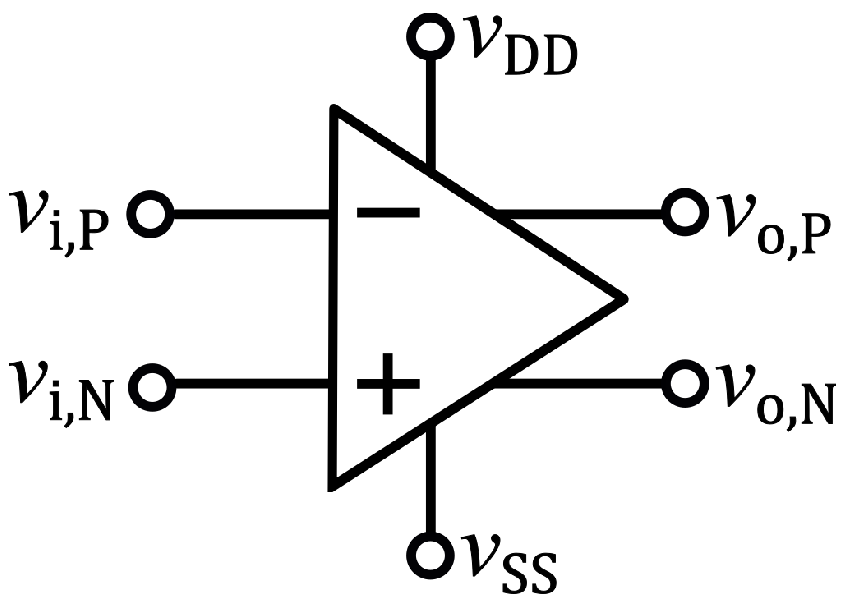
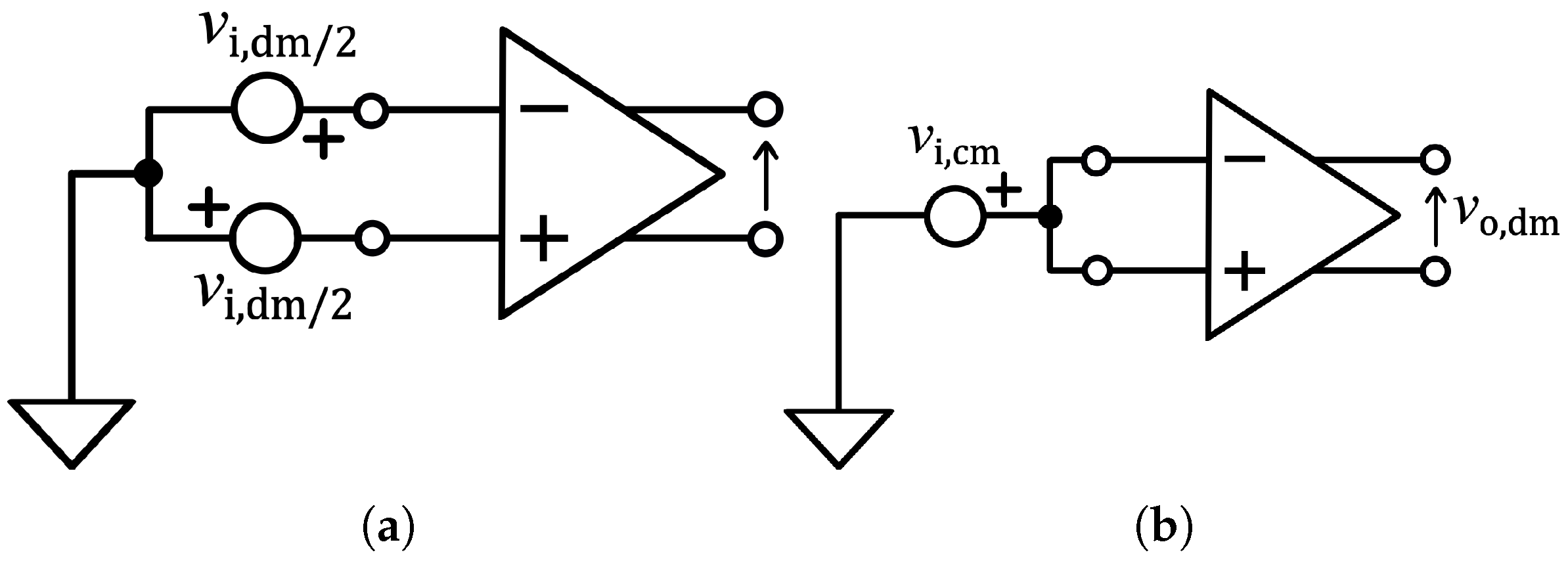
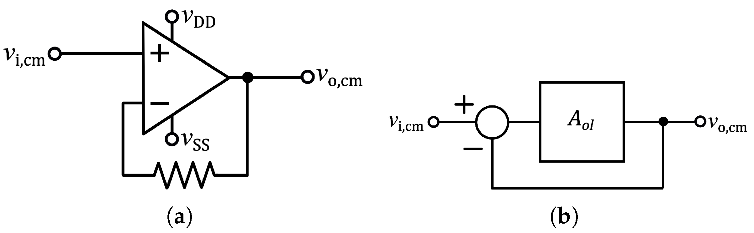
2.1. CMRR of a Fully Differential Active Circuit

As shown in Figure 2, an FD active circuit has four inputs—two for the signals ( v i , P and v i , N ) and two for the power supplies ( v D D and v S S )—as well as two signal outputs ( v o , P and v o , N ). Assuming an appropriate operating point, the small-signal inputs ( v i , p , v i , n , v d d , and v s s ) and outputs ( v o , p and v o , n ) can be defined. Additionally, the differential- and common-mode input voltages can be expressed as v i , d m = v i , p v i , n and v i , c m = ( v i , p + v i , n ) / 2 , respectively; similarly, the differential- and common-mode output voltages are defined as v o , d m = v o , p v o , n and v o , c m = ( v o , p + v o , n ) / 2 , respectively. Following the notation of Säckinger and Guggenbühlin [18], the relationship between the inputs and outputs can be expressed in the Laplace domain as
V o , d m ( s ) = A d m d m ( s ) V i , d m ( s ) + A c m d m ( s ) V i , c m ( s ) + A d d d m ( s ) V d d ( s ) + A s s d m ( s ) V s s ( s ) ,
V o , c m ( s ) = A c m c m ( s ) V i , c m ( s ) + A d m c m ( s ) V i , d m ( s ) + A d d c m ( s ) V d d ( s ) + A s s c m ( s ) V s s ( s ) .
where A n m denotes the transfer function from input n to output m. To simplify the equations, the dependence on the Laplace variable s will be omitted from all expressions hereafter.
Assuming that the power supply voltages are constant, they are considered zero in the small-signal analysis, i.e., v d d = v s s = 0 . Therefore, (1) can be simplified and rewritten as
V o , d m = A d m d m V i , d m + V i , c m C M R R ,
where the CMRR is defined as
C M R R = A d m d m A c m d m .
To calculate the CMRR, it is necessary to obtain both transfer functions. The differential-to-differential gain ( A d m d m ), which defines the function of the circuit (e.g., amplifier or filter), can be evaluated theoretically and experimentally using the scheme in Figure 3a since v i , c m is connected to ground and the only small-signal input is v i , d m . Conversely, the common-to-differential gain ( A c m d m ), which represents the undesired mode transformation that occurs inside the amplifier, can be evaluated using the scheme in Figure 3b, where v i , d m is short-circuited and the only small-signal input is v i , c m .

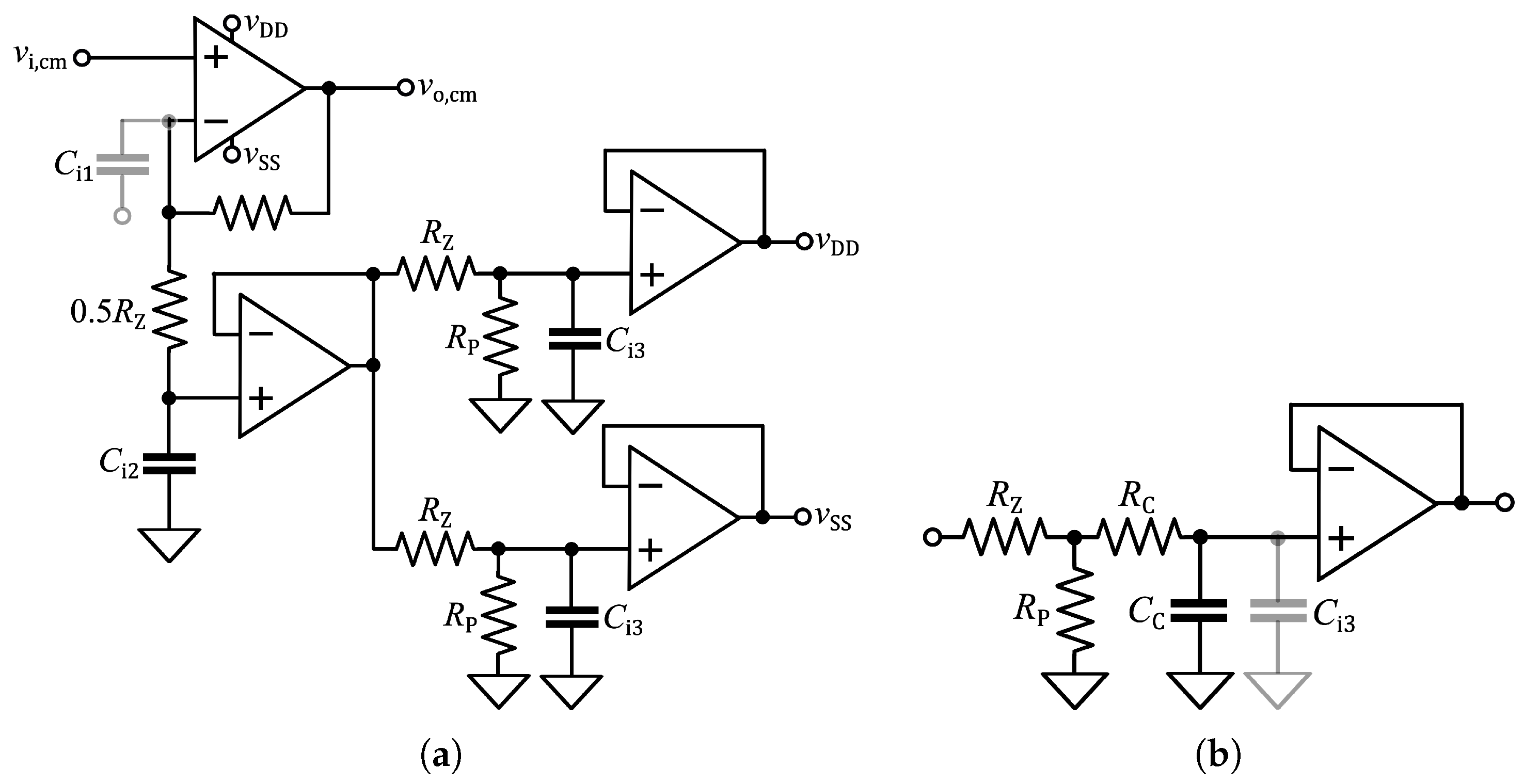
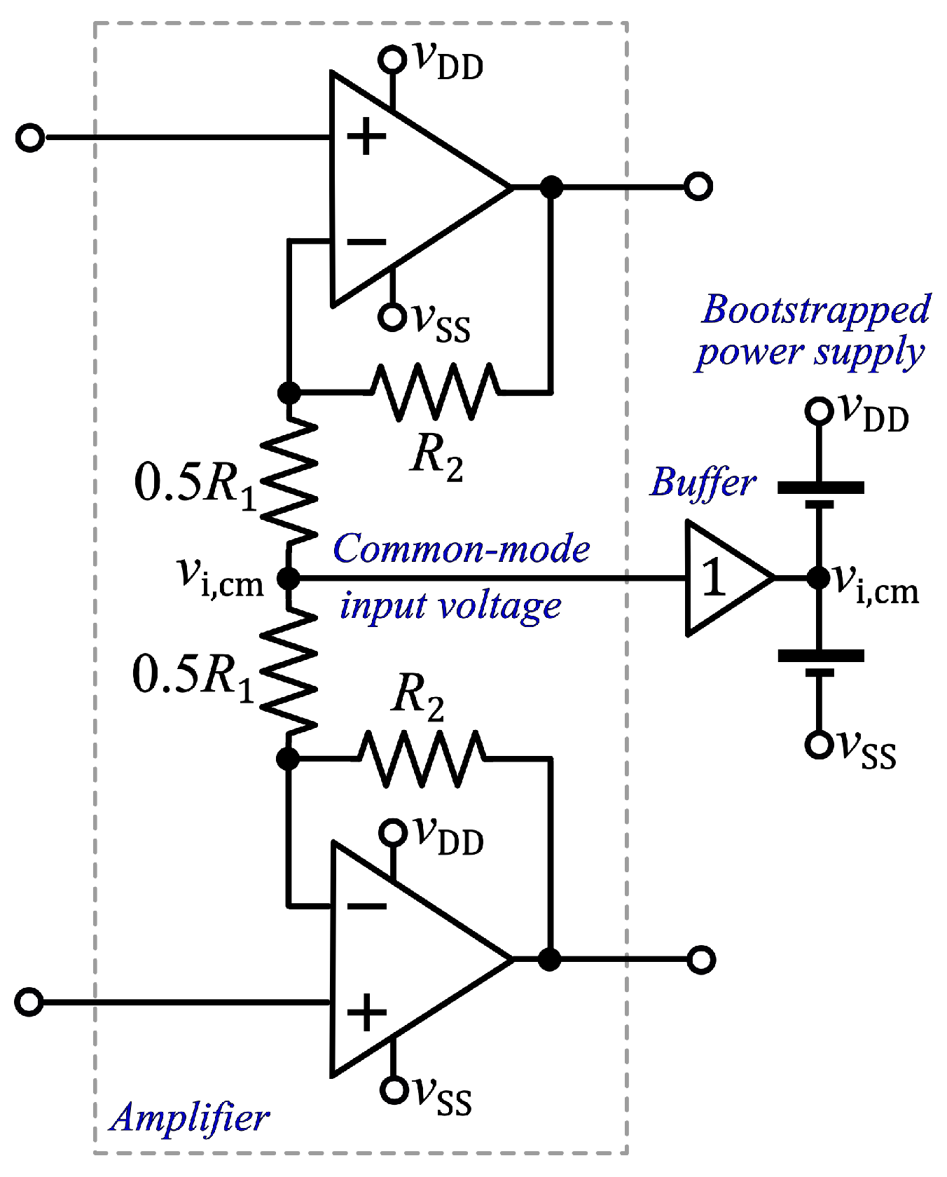
2.2. CMRR Enhancement by Power Supply Bootstrapping

To avoid CMRR degradation due to passive component imbalances, all explicit ground connections should be removed following the technique described by Spinelli et al. [4]. In this way, the CMRR depends only on mismatches in the parameters of the active components. For example, for the typical FD active amplifier shown in Figure 1b, the CMRR can be approximated as follows [3]:
C M R R 1 ( A o l 1 1 A o l 2 1 ) ( C M R R 1 1 C M R R 2 1 ) ,
where A o l 1 and C M R R 1 are the parameters of OA1, and A o l 2 and C M R R 2 are the parameters of OA2.
Despite this limitation, it is possible to increase the CMRR by using the PSB technique. If v i , c m is incrementally fed back to the power supply nodes, i.e., v d d = v s s = v i , c m , and v i , d m is short-circuited, (1) becomes
V o , d m = A c m d m + A d d d m + A s s d m V i , c m .
As demonstrated by Säckinger and Guggenbühlin [18], an FD active circuit without grounded passive components satisfies the following condition:
A c m d m + A d d d m + A s s d m = 0 ,
so that the differential output voltage given by (6) becomes zero. Therefore, when v i , c m is applied to the circuit, no mode transformation occurs: the CMRR becomes infinite. In practice, however, parasitic impedances—mainly capacitances—connect the circuit nodes to ground and the power-supply voltages do not exactly follow v i , c m . As a result, the CMRR is not infinite, but very high values can still be achieved.
Figure 4 shows a scheme for applying PSB to the typical FD amplifier shown in Figure 1b. In this case, v i , c m can be estimated from the circuit by splitting the gain resistor R 1 without degrading the input impedance and feeding it back to the midpoint of the dual DC supply voltages. A buffer can be used to avoid loading effects. Now, the CMRR depends only on the accuracy with which v d d and v s s follow v i , c m , which is limited by stability issues [19].

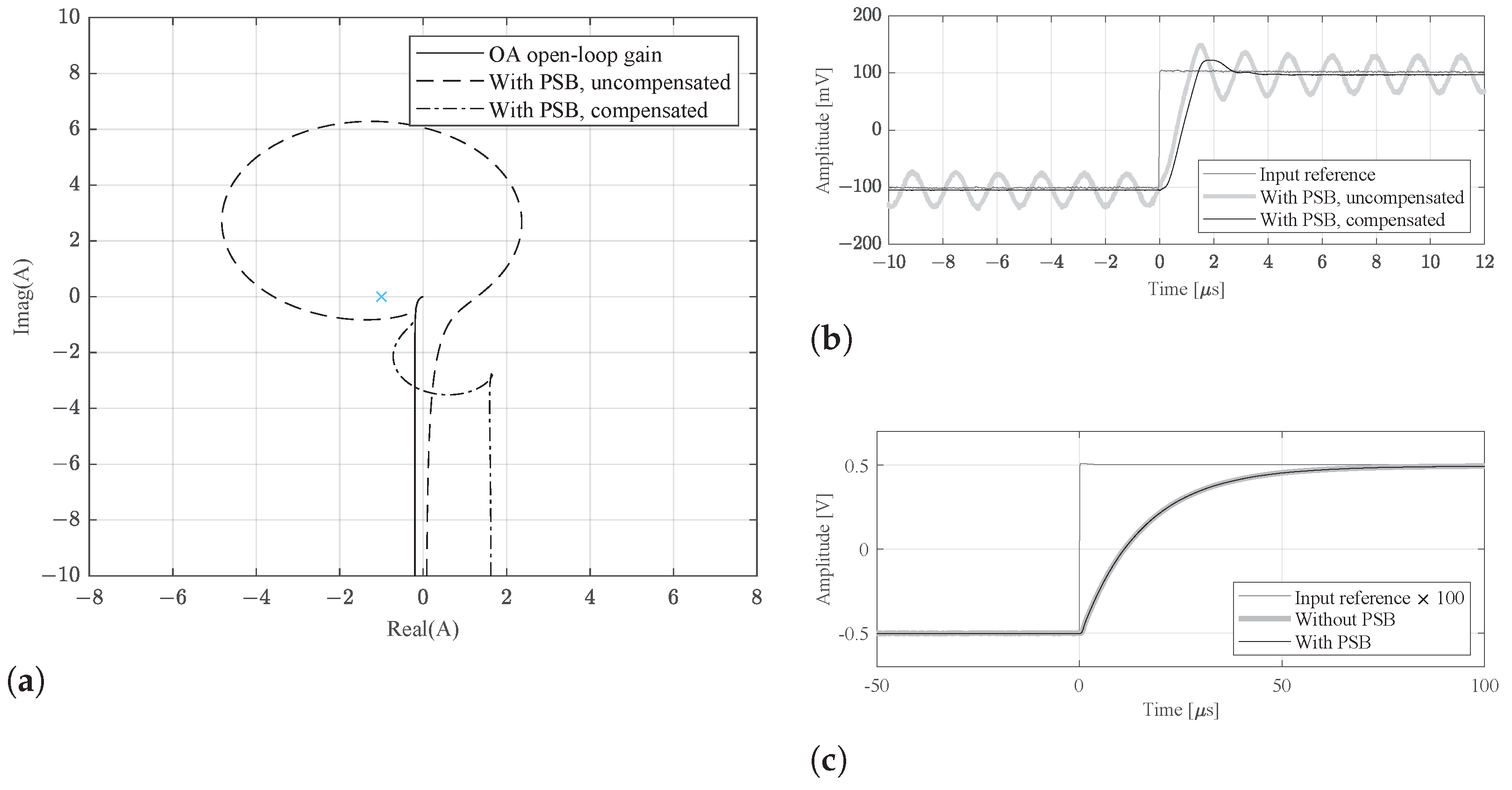
2.3. Stability Analysis

Even in amplifiers that are stable under both differential- and common-mode operations, the application of PSB is known to introduce stability concerns [12]. However, no formal stability analysis has been presented specifically for FD circuits.
A broad class of FD circuits exhibits an axis of symmetry, enabling the application of the bisection theorem [20] to derive differential- and common-mode half-circuits. This approach decouples the analysis and simplifies the overall circuit evaluation. Furthermore, because FD circuits avoid ground connections, they inherently exhibit a unity common-to-common gain ( A c m c m = 1 ). As a result, the common-mode half-circuit ideally presents a closed-loop gain equal to one.
The common-mode half-circuit corresponding to the circuit in Figure 1b is represented in Figure 5. Since this class of circuits implements unity gain feedback, the stability analysis methods developed in previous work for power supply bootstrapped buffer circuits [19] can be directly applied. Accordingly, the open-loop transfer function of the complete bootstrapped system ( G o l , P S B ) depends on the A o l of the OA, coupled with any other transfer elements on the direct path, and on the transference from each supply node to the output ( A d d c m and A s s c m ) as follows:
G o l , P S B = A o l 1 + α s s A s s c m + α d d A d d c m .
Equation (8) can be simplified in the case where one of the power supply transfer functions, A s s d m or A d d d m , dominates, i.e., it is approximately equal to 1. For instance, if the dominant transfer corresponds to the low-rail supply, then A s s c m 1 , and (8) simplifies to
G o l , P S B A o l 1 + α s s A s s c m .
This framework allows for applying a compensation on the problematic rail, accepting a slight degradation in the bootstrapping circuit. For example, a low-pass compensator placed before the critical zero crossover region can be used to ensure circuit stability. Equation (9) also facilitates determining an appropriate value for the compensation network, which can be numerically tested prior to implementation (see Appendix A). It is worth noting that the loading impedances have been neglected in this analysis.

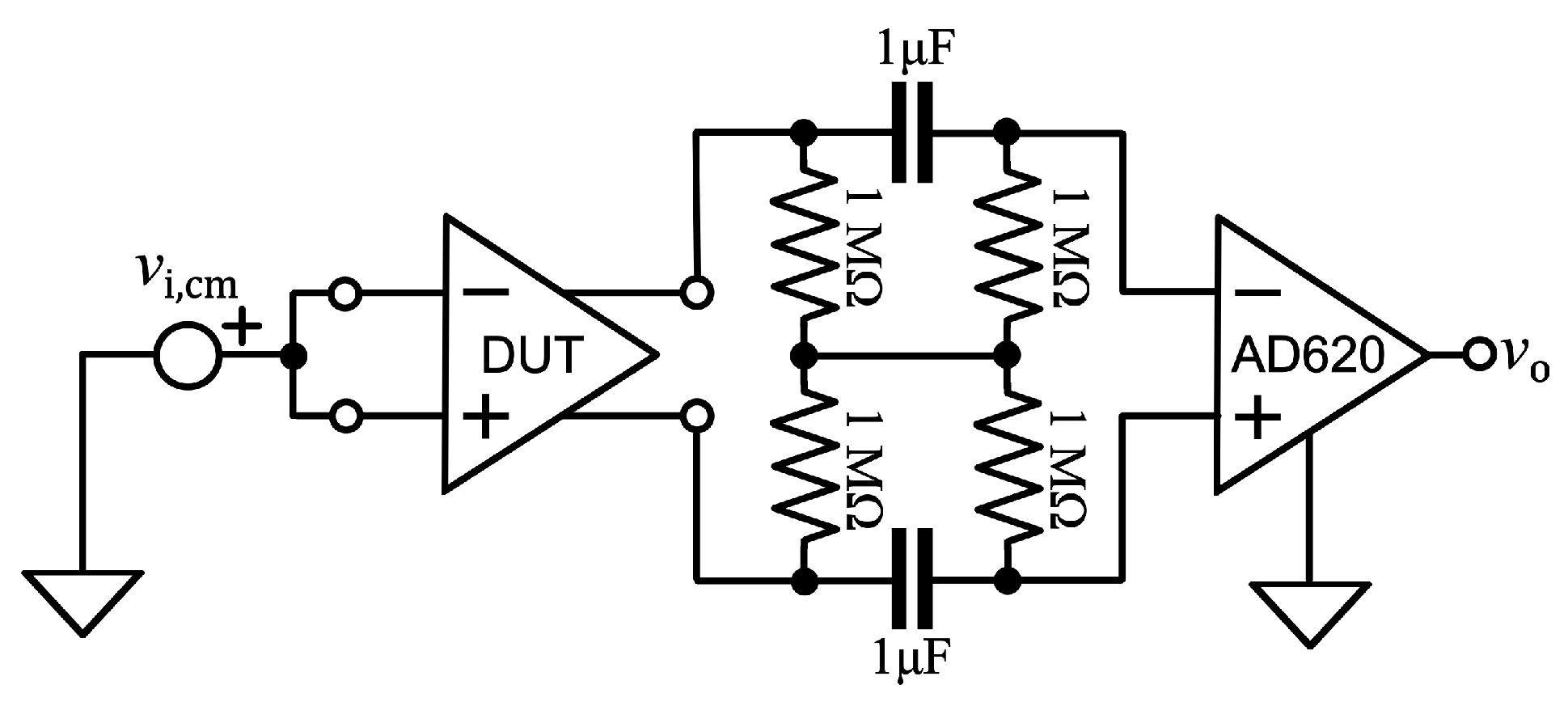
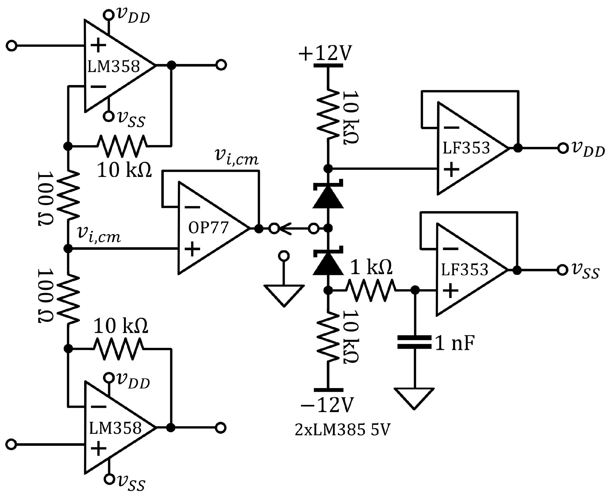
2.4. Experimental Setup
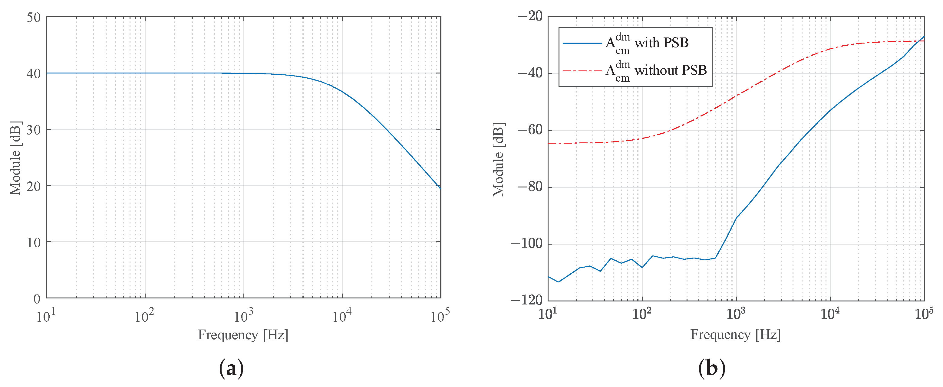
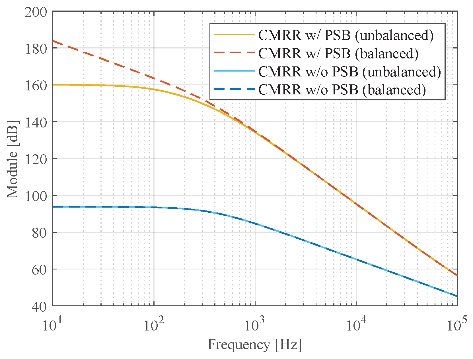
The proposed bootstrapped scheme shown in Figure 4 was implemented using the practical circuit depicted in Figure 6, where it employed discrete components and off-the-shelf general purpose OAs. The LM358 OAs of the FD amplifier were powered with ± 5 V provided by two LM385 zener diodes followed by two buffers implemented with LF353 OAs. A switch connected to the midpoint of the zener diodes allowed for activation or deactivation of the PSB technique. When the midpoint of the zeners was connected to ground, the supply nodes v D D and v S S provided only the DC voltage, and the amplifier operated without PSB. Conversely, when the midpoint was connected to the output of the buffer implemented with the OP77 OA, the PSB technique was activated by feeding back v i , c m . The zener diodes, as well as the LF353 and OP77 OAs, were powered by a ± 12 V bench DC power supply.
The differential-to-differential gain A d m d m , which was designed to be 40 dB, was experimentally measured using the setup shown in Figure 3a. The differential-mode signals were generated and measured with a Stanford Research Systems SR865A lock-in amplifier via synchronous demodulation. On the other hand, calculating the CMRR required measuring the common-to-differential transfer function ( A c m d m ). Since high CMRR values are expected, using only the setup shown in Figure 3b may result in output amplitudes that are too small to measure accurately. Therefore, an AD620 instrumentation amplifier with a gain of 40 dB was inserted before the lock-in amplifier, and the resulting single-ended output amplitude was measured. For a detailed analysis, see Appendix B. To minimize the external interference, the PCB was enclosed in a grounded metal box. The measured data were post-processed using MATLAB R2016a.

3. Results

The amplifier from Figure 6 was built with off-the-shelf components and 5% tolerance resistors in order to obtain the boosted CMRR using PSB. First, the method for the stability design was implemented. The numerical simulation using (A1) yielded the results shown in Figure 7a, where it was found that the proposed compensation with a 159 k Hz low-pass filter on α SS could produce a stable transference. The Nyquist plot was zoomed near the critical ( 1 , 0 ) point and it was seen that the transfer function that previously encircled ( 1 , 0 ) now followed a stable trajectory. Next, measurements of the step transient showed that the circuit was indeed stable in differential and common modes. Figure 7b presents the common-mode step response before compensation (light gray line), which resulted in a markedly oscillatory behavior. After the compensation, the output followed the reference step. The differential-mode step response was also measured to compare the performance of the amplifier before and after applying PSB. The result shows (Figure 7c) that the response was stable and identical.
Next, the amplifier was characterized and the measured curves are shown in Figure 8. Figure 8a shows the A d m d m gain and Figure 8b shows the A d m c m gain with and without bootstrapping enabled. From the curves in Figure 8, the CMRR could be calculated using (4). The results can be seen in Figure 9.
To analyze the effects of imbalances, the topology was further simulated using TINA software (Version 9.3.200.277 SF-TI) (Texas Instruments) and its embedded LM358 macromodel. In circuits like the one shown in Figure 1b, which have no explicit connection to ground, the CMRR does not depend on mismatches in the passive components but rather on active parameters, such as the CMRR and open-loop gain of the operational amplifiers. Therefore, a mismatch was intentionally introduced between the operational amplifiers to achieve a CMRR of approximately 90 dB under a perfect resistor balance and without the use of PSB. This was achieved by connecting a resistor in parallel with the main current source of one of the amplifiers, thereby altering its CMRR and open-loop gain. The modified circuit models are provided as Supplementary Material.
Using the modified versions of the circuit, the impact of the passive component imbalance was evaluated. Figure 10 shows the simulated CMRR with and without PSB under two conditions: first, with perfect matching of the passive components, and then with a ± 10 % mismatch in resistors R 1 and R 2 .
For the circuit without PSB, as expected, there were no significant differences in the CMRR between the balanced and imbalanced resistor cases. When the PSB technique was applied, the CMRR due to the OA mismatches improved and the impact of resistor imbalances became noticeable at low frequencies, where the tiny input currents of the OAs produced a differential output voltage when flowing across the imbalanced resistors. However, the degradation was only evident at extremely high CMRR values (above 150 dB), which are beyond what is typically relevant in practical applications.

4. Discussion

The theoretical framework provided by [18] enabled further development of the high-CMRR fully differential circuit design method proposed in [4], offering a rationale for the improvement achieved through power supply bootstrapping. The technique of replacing ground connections with common-mode supplies is not immediately apparent in circuits based on operational amplifiers, as these connections are concealed within the power supply terminals. However, they remain a source of CMRR degradation. In this work, it was shown that power supply bootstrapping provides an effective means of mitigating this issue.
A typical fully differential amplifier was complemented by CM PSB. As is derived from the results (Figure 9), the elimination of the residual connections to ground through the power supply rails, which for general applications can be regarded as second-order effects, effectively increased the CMRR. In the presented example, the CMRR was augmented from 90 dB to over 130 dB at 1 kHz.
This improvement is in line with previous works that implement the technique. The CMRR of a fully differential circuit can be improved by various methods, such as including a trimming loop in chopper amplifiers [21] or using a replica of the common-mode input voltage to drive internal circuit nodes, allowing for CMRR values up to 130 dB at 50 Hz [16]. This limit can be surpassed by using power supply bootstrapping and commercial components [12], reaching CMRRs above 140 dB at 50 Hz, but potential stability issues arise. The proposed methodology allows for CMRR values above 140 dB to be achieved at frequencies down to a few kHz, even when using general purpose operational amplifiers, such as the LM358, while ensuring circuit stability.
The CMRR improvement provided by the PSB is mainly limited by stability issues, as was shown with the presented design case example. The technique works very well at frequencies up to several tens of kilohertz, making it well-suited for biomedical and instrumentation applications. Potential applications of the method to higher bandwidths must consider that the critical frequency range affecting stability is around the 0 dB crossover frequency of the non-bootstrapped amplifier. Hence, the bootstrap compensation, which degrades the CMRR improvement, needs to take place at most at that frequency. Therefore, as a higher bandwidth device is used, the problematic frequencies move to a higher range and the operating range of the PSB CMRR boosting circuit could be extended.
The proposed methodology could be extended to other circuits, such as fully differential filters [22] or low-noise neural amplifiers [15], to improve their CMRR by bootstrapping the power supply of the first stage. If this stage provides a significant gain, the subsequent stages do not contribute substantially to the overall CMRR [3] and PSB can be used only in the front end to reduce the power consumption.
The PSB circuitry implies a cost in terms of power consumption and increases the part-count or area overhead depending on the implementation. Therefore, the technique is best-suited for design cases where obtaining very high CMRR values justifies the imposed trade-off. However, as it enables the achievement of high CMRR values without functional trimmings, it may offer a reduction in the complexity and cost of the circuit production.
Although previous works present practical implementations of this strategy, in this paper, we present a theoretical framework both for the CMRR improvement and the circuit stability, and demonstrate it through a practical example. Moreover, in this work, for the first time, the theoretical framework for PSB circuit stability [19] was translated to FD circuits by finding a simple application of the principles to obtain a circuit with a stable CM.

Supplementary Materials

The following supporting information can be downloaded from https://www.mdpi.com/article/10.3390/chips4020027/s1: TINA model to obtain the common mode-to-differential mode gain (GDC_LM358.TSC), TINA model to obtain the differential mode-to-differential mode gain (GDD_LM358.TSC), simulation results obtained with TINA (GDCBalancedConPSB.txt, GDCBalancedSinPSB.txt, GDCUnbalancedConPSB.txt, GDCUnbalancedSinPSB.txt, GDDBalancedSinPSB.txt, GDDUnbalancedSinPSB.txt), and MATLAB script for Figure 10 (SimulationCMRR_Booster.m).

Author Contributions

Conceptualization, E.M.S.; methodology, E.M.S., V.A.C., F.N.G. and M.A.H.; validation, V.A.C. and M.A.H.; investigation, E.M.S., V.A.C., F.N.G. and M.A.H.; writing—original draft preparation, E.M.S., V.A.C. and F.N.G.; writing—review and editing, E.M.S., V.A.C., F.N.G. and M.A.H.; supervision, E.M.S.; project administration, E.M.S. All authors have read and agreed to the published version of the manuscript.

Funding

This research was funded by CONICET grant number PIP0323 and UNLP grant number PIP-I254.

Institutional Review Board Statement

Not applicable.

Informed Consent Statement

Not applicable.

Data Availability Statement

The raw data supporting the conclusions of this article will be made available by the authors on request.

Conflicts of Interest

The authors declare no conflicts of interest. The funders had no role in the design of this study; in the collection, analyses, or interpretation of the data; in the writing of this manuscript; or in the decision to publish the results.

Appendix A

The common-mode half-circuit for the FD amplifier from Figure 6 is shown in Figure A1a. The symmetric amplifier was bisected, with R 1 divided into two. The bootstrapping circuit on the other hand was duplicated along the symmetry axis and appears replicated in the common-mode circuit.
Figure A1. Measured transfer functions for the circuit of Figure 6: (a) half-circuit with high/low rail bootstrapping subcircuit for common-mode PSB stability analysis; (b) added low-pass compensation to the V S S rail degrading the bootstrap at high frequcency. C i 3 is rendered negligible by C c .
Chips 04 00027 g0a1
Note that in the circuit of Figure A1a, the zener diode was replaced by its series dynamic resistance R Z . At the same time, relevant parasitic components were included. However, the input capacitance of the amplifier’s OA C i 1 is made negligibly small by the CM bootstrapping; therefore, it has no impact in the transference. Likewise, the amplifiers’ OA had all nodes in the common mode, and thus, no current circulated through R 2 , making it effectively a buffer.
The PSB transference from the PSB input to the high and low rail α d d and α s s can be obtained by inspection from Figure A1a:
α d d / s s = v d d / s s v i , c m = 1 ( 1 + s C i 2 R 1 / 2 ) A 2 ( 1 + A 2 ) ( R z R p ) / R z ( 1 + s C i 3 R z R p ) A 3 ( 1 + A 3 )
The circuit was implemented using an LM358 OA for its main amplifier. This OA has a P S R R curve closely following its A o l curve; therefore, A s s c m 1 and a compensation can be simply applied to the low rail [19]. Figure A1b shows the modified circuit where a low-pass filter composed of R c and C c was added, resulting in the following transfer:
α s s , c o m p = v s s v i , c m = 1 ( 1 + s C i 2 R 1 / 2 ) A 2 ( 1 + A 2 ) ( R z R p ) / R z ( 1 + s C c R z R p R c ) A 3 ( 1 + A 3 ) .
Equations (A1) and (A2) are necessary to obtain the complete expression for the open loop transfer and derive the stability of the system. The open-loop transfers of the common-mode buffer OA A 1 and the PSB driver OAs A 2 were included because the gain bandwidth products of these OAs are close to that of the main amplifier OA; therefore, their dynamic near the 0 dB crossover is relevant, even if they are included as closed-loop circuits. Another relevant consideration is the dynamic resistance R Z since by depending on the device, in this case, an LM385, its value can be non-negligible in the transfer function. For the numerical analysis performed in this work, R Z was assigned a frequency-dependent value adjusted to the curve reported in the data sheet of the device.

Appendix B

To experimentally determine the CMRR of the proposed circuit, it was necessary to measure the common-to-differential transfer function ( A c m d m ). For this purpose, an AD620 instrumentation amplifier with a gain of 40 dB was incorporated to amplify the signal and convert it to a single-ended output, as shown in Figure A2. This configuration enabled the more accurate measurement of very low output signal amplitudes when the CMRR was high. A high-pass filter was included to block the offset from the first stage to saturate the subsequent stage.
Figure A2. Schematic of the CMRR measurement experimental setup.
Chips 04 00027 g0a2
Considering only the differential- and common-mode input voltages in the small-signal analysis, the FD amplifier produced the following output voltages:
V o , d m = A d m d m V i , d m + A c m d m V i , c m ,
V o , c m = A c m c m V i , c m + A d m c m V i , d m .
The AD620 instrumentation amplifier then took these signals as the input and generated a unique single-ended output v o :
V o = A d m o V o , d m + A c m o V o , c m ,
where A d m o and A c m o are the differential-to-output and common-to-output gains of the AD620, respectively. By substituting (A3) and (A4) into (A5), and factoring out the gains A d m d m and A d m o , the output voltage can be approximated as
V o A d m d m ( s ) A d o ( s ) ( V i , d m + V i , c m C M R R 1 + V i , c m C M R R 2 A d m d m )
Therefore, the total CMRR of the system is
C M R R T 1 C M R R 1 1 + ( C M R R 2 A d m d m ) 1
If C M R R 2 A d m d m C M R R 1 , then the C M R R T measured using the AD620 is approximately equal to C M R R 1 of the FD amplifier.

References

  1. Pallás-Areny, R.; Webster, J.G. Common mode rejection ratio in differential amplifiers. IEEE Trans. Instrum. Meas. 1991, 40, 669–676. [Google Scholar] [CrossRef]
  2. Casas, O.; Spinelli, E.M.; Pallas-Areny, R. Fully differential AC-coupling networks: A comparative study. IEEE Trans. Instrum. Meas. 2008, 58, 94–98. [Google Scholar] [CrossRef]
  3. Pallás-Areny, R.; Webster, J.G. Analog Signal Processing; John Wiley & Sons: Hoboken, NJ, USA, 1999. [Google Scholar]
  4. Spinelli, E.M.; Hornero, G.; Casas, O.; Haberman, M. A design method for active high–CMRR fully–differential circuits. Int. J. Instrum. Technol. 2012, 1, 103–113. [Google Scholar] [CrossRef]
  5. Spinelli, E.M.; Guerrero, F.N.; Garcia, P.A.; Catacora, V.A.; Haberman, M.A. A fully-differential biopotential amplifier with a reduced number of parts. IEEE Trans. Instrum. Meas. 2022, 71, 2006908. [Google Scholar] [CrossRef]
  6. Andrew, A.M. Differential amplifier design. Wirel. Eng. 1955, 33, 73–79. [Google Scholar]
  7. Blume, R.J. Bootstrapped Differential Amplifier with Reduced Common-Mode Effects. Rev. Sci. Instrum. 1958, 29, 122–124. [Google Scholar] [CrossRef]
  8. McClellan, A.D. Extracellular amplifier with bootstrapped input stage results in high common-mode rejection. Med. Biol. Eng. Comput. 1981, 19, 657–658. [Google Scholar] [CrossRef] [PubMed]
  9. Kootsey, J.M.; Johnson, E.A. Buffer amplifier with femtofarad input capacity using operational amplifiers. IEEE Trans. Biomed. Eng. 1973, BME-20, 389–391. [Google Scholar] [CrossRef] [PubMed]
  10. Bergveld, P. Alternative design of a unity-gain follower with buffer. IEEE Trans. Biomed. Eng. 1978, BME-25, 567–568. [Google Scholar] [CrossRef]
  11. Maji, S.; Burke, M.J. A bootstrapping technique to boost input impedance of ECG recording amplifiers. In Proceedings of the 2022 IEEE International Instrumentation and Measurement Technology Conference (I2MTC), Ottawa, ON, Canada, 16–19 May 2022; pp. 1–6. [Google Scholar] [CrossRef]
  12. Stitt, M. Boost Instrument Amp CMR with Common-Mode Driven Supplies; Technical report, Burr-Brown Application Bulletin SBOA014; Burr-Brown Corporation: Tucson, AZ, USA, 1997. [Google Scholar]
  13. Jooq, M.K.Q.; Behbahani, F.; Moaiyeri, M.H. An ultra-efficient recycling folded cascode OTA based on GAA-CNTFET technology for MEMS/NEMS capacitive readout applications. AEU-Int. J. Electron. Commun. 2021, 136, 153773. [Google Scholar] [CrossRef]
  14. Koo, N. Design of Low Power and Low Noise Instrumentation Amplifier for Biopotential Acquisition: A Review. IEEE Access 2025, 13, 23359–23370. [Google Scholar] [CrossRef]
  15. Fava, A.; Centurelli, F.; Monsurrò, P.; Scotti, G. A Compact Low-Power Chopper Low Noise Amplifier for High Density Neural Front-Ends. Sensors 2025, 25, 1157. [Google Scholar] [CrossRef] [PubMed]
  16. Zhang, S.; Zhou, X.; Gao, C.; Li, Q. A 130-dB CMRR instrumentation amplifier with common-mode replication. IEEE J. Solid-State Circuits 2021, 57, 278–289. [Google Scholar] [CrossRef]
  17. Yan, F.; Liu, J. Analog front-end input-impedance boosting techniques for bio-potential monitoring—A review. IEEE Trans. Instrum. Meas. 2024, 73, 2002214. [Google Scholar] [CrossRef]
  18. Säckinger, E.; Goette, J.; Guggenbühl, W. A general relationship between amplifier parameters, and its application to PSRR improvement. IEEE Trans. Circuits Syst. 1991, 38, 1173–1181. [Google Scholar] [CrossRef]
  19. Guerrero, F.N.; Spinelli, E.M. Stability of power supply bootstrapped unity-gain buffers. IEEE Trans. Circuits Syst. II Express Briefs 2022, 69, 4258–4262. [Google Scholar] [CrossRef]
  20. Midlebrook, R. Differential Amplifiers; John Wiley and Sons, Inc.: Hoboken, NJ, USA, 1963. [Google Scholar]
  21. Zhang, S.; Zhou, X.; Gao, C.; Li, Q. An AC-coupled instrumentation amplifier achieving 110-dB CMRR at 50 Hz with chopped pseudoresistors and successive-approximation-based capacitor trimming. IEEE J. Solid-State Circuits 2020, 56, 277–286. [Google Scholar] [CrossRef]
  22. Massarotto, M.; Casas, O.; Ferrari, V.; Pallas-Areny, R. Improved fully differential analog filters. IEEE Trans. Instrum. Meas. 2007, 56, 2464–2469. [Google Scholar] [CrossRef]
Figure 1. Examples of FD circuits: (a) passive circuit without components connected to ground [2]; (b) active circuit with no explicit connections to ground but with two implicit ones established through its power supply nodes [3].
Chips 04 00027 g001
Figure 2. FD active circuit with all terminals labeled.
Chips 04 00027 g002
Figure 3. Circuit diagrams for determining the CMRR of an FD circuit: (a) differential-to-differential transfer measurement scheme; (b) common-to-differential transfer measurement scheme.
Chips 04 00027 g003
Figure 4. Schematic of the FD active circuit from Figure 1b adapted for the PSB application.
Chips 04 00027 g004
Figure 5. Common-mode half-circuit from the circuit in Figure 1b: (a) circuit scheme; (b) block diagram representation.
Chips 04 00027 g005
Figure 6. Practical implementation of the FD amplifier with PSB.
Chips 04 00027 g006
Figure 7. (a) Nyquist plot for stability analysis. The critical ( 1 , 0 ) point is marked with an × symbol. (b) Temporal step response measurements before and after the compensation for CM. (c) Temporal step response measurements before and after PSB.
Chips 04 00027 g007
Figure 8. Measured transfer functions for the circuit of Figure 6: (a) differential-to-differential gain A d m d m ; (b) common-to-differential gain A c m d m .
Chips 04 00027 g008
Figure 9. CMRR measurements of the FD amplifier with and without PSB, and the measurement limits of the utilized instrumentation.
Chips 04 00027 g009
Figure 10. Simulation results testing a ± 10 % imbalance in the passive components with and without power supply bootstrapping.
Chips 04 00027 g010
Disclaimer/Publisher’s Note: The statements, opinions and data contained in all publications are solely those of the individual author(s) and contributor(s) and not of MDPI and/or the editor(s). MDPI and/or the editor(s) disclaim responsibility for any injury to people or property resulting from any ideas, methods, instructions or products referred to in the content.

