Abstract
This paper presents the design analysis of a low-power wideband single-ended CMOS low-noise amplifier (LNA). The proposed topology is based on a modified current- reuse circuit, in which two-stage common-source (CS) amplifiers consume the same DC current and are isolated from each other by large MIMCAPs, which results in good performance with low power consumption. The proposed circuit achieves a bandwidth of 2.5 GHz, suitable for several wireless communication standards such as GSM, WLAN, and Bluetooth. In the first stage, a current-reuse circuit with shunt feedback is used to satisfy input impedance matching and signal amplification with minimal noise injection. A common source (CS) with a source follower circuit forms the second stage to improve the noise figure (NF), harmonic distortion, and output impedance matching. The proposed LNA is designed in 65 nm CMOS technology and covers a frequency range of 0.17–2.68 GHz. The proposed LNA achieves a maximum gain of 17.24 dB, a minimum NF of 2.67 dB, a maximum IIP3 of −14.9 dBm, and input and output return losses of less than −10 dB. The power consumption of the proposed LNA is 3.52 mW from a 1 V power supply, and the core area is 0.3 mm2.
1. Introduction
Wideband low-noise amplifiers (LNAs) are the main building blocks in a receiver system to cover multiple wireless communication standards. LNAs should amplify the weak signal received by the antenna with a flat response and minimal noise injection. Also, input impedance and linearity over the frequency bandwidth are two important parameters of wideband LNAs, used to prevent signal reflections and harmonic distortion [1]. However, in the design of wideband LNAs, there is a trade-off between the above-mentioned parameters and power consumption [2]. Recently, low-power designs have received a lot of attention, as most of the systems are powered by only a single lithium battery, which must work for several days (mobile phone) or even a year (medical devices). Therefore, designing low-power circuits is a hot topic of research in academia and is a major challenge for RF designers [3]. LNAs can either be single-ended or differential. Although single-ended LNAs have lower gain and linearity, they have good stability and low-noise performance, whereas differential LNAs are excellent at achieving high gain and better linearity [4]. Common-gate (CG) and common-source (CS) circuits are used either individually or in combination for differential and single-ended LNA designs [5]. Although CG topology shows the best performance for wideband LNAs because of its low input impedance independent of frequency, it needs higher power consumption to satisfy input impedance matching and the noise figure (NF). Therefore, CG topology is not often used alone for low-power circuits. A CS with shunt feedback is another choice in designing wideband LNAs and consumes more power to achieve high gain and a low NF, necessitating current-reuse techniques [6].
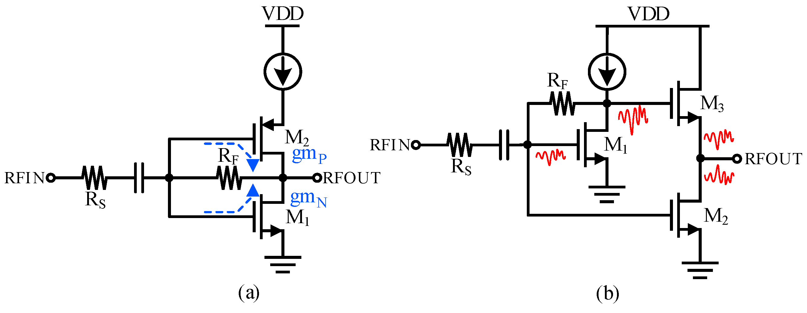
The noise cancellation technique is another method for reducing thermal noise with low power consumption, as reported in 2004 [7]. Figure 1a shows conventional current-reuse with shunt feedback [2], and 1b shows a noise cancellation LNA [7]. In [8], a differential LNA was reported that shows good linearity. In the reported work, using a combination of CS, CG, and a cross-couple structure between the positive and negative outputs, linearity was improved without a gain reduction over the entire bandwidth. However, the requirement of an external RF choke, an additional buffer, and high power consumption of around 12 mW are its limitations. The authors of [9] reported a differential LNA by combining CG and CS in 65 nm CMOS. Although the gain was high, high power consumption of 19.8 mW made it unsuitable for low-power devices. A low-power differential LNA using CG and CS was reported in [10], which presented a differential LNA with a frequency range of 0.05 to 1.3 GHz. However, an external RF choke was used, similar to [9,10]. In [11], a differential LNA for sub-GHz applications with a low power of 3 mW was presented, but the minimum NF of 3.6 dB was not suitable for noise-sensitive applications. In [12], an inductor-less wideband LNA that covered 0.18 to 2 GHz was reported. The presented circuit used a combination of CG and CS topology with transconductance (gm) and was boosted by using a cross-couple structure between differential nodes. However, the results were reported under an unmatched output impedance. If the buffer current is calculated, the results become poor. Reference [13] reported a noise and distortion cancellation LNA with single-ended output that achieved reasonable results with an ultra-low power (under 1 mW) by handling shunt feedback and the feedforward technique. Although the reported circuit consumes ultra-low amounts of power, it needs a buffer network to measure, and the minimum NF of 4.45 dB is high. Yunyou Pu and Wei Li reported a differential wideband LNA from 0.2 to 3.2 GHz by using CS and CG and a noise cancellation technique [14]. Although they achieved a high gain and a minimum NF of 1.4 dB, the power dissipation was 17.4 mW, which is very high for low-power applications. In [15], a single-ended LNA with CG, current-reuse and noise cancellation circuits for low-voltage and low-power applications was presented. Though the results were acceptable, the area and power of buffer circuit was not calculated. In [16], a differential wideband LNA using noise and distortion cancellation techniques with a 1.6 GHz bandwidth was presented. A minimum NF of 1.1 dB was reported; however, its power consumption of 9.1 mW is high for low-power systems.

Figure 1.
(a) Conventional current-reuse LNA and (b) noise cancellation technique LNA.
This paper presents a single-ended wideband LNA for low-power applications which covers the frequency range from 0.17 to 2.68 GHz. The proposed circuit consists of two stages. The first stage employs a current-reuse topology incorporating both shunt feedback and series inductive peaking techniques to achieve flat gain with low NF while satisfying input impedance matching requirements. The second stage implements a combined CG and CS configuration that functions as a buffer network while simultaneously improving NF and linearity performance. Both stages share the same DC bias current and are isolated through a large metal–insulator–metal capacitor (MIMCAP). Due to the current-reuse technique, the proposed LNA achieves significant power consumption reduction. Furthermore, the output impedance is matched to a 50 Ω load without requiring an additional buffer network for measurement. The paper is organized as follows. Section 2 analyzes the proposed LNA structure in detail. Section 3 presents the post-layout simulation results, and finally Section 4 provides the conclusion.
2. Analysis of the Proposed LNA
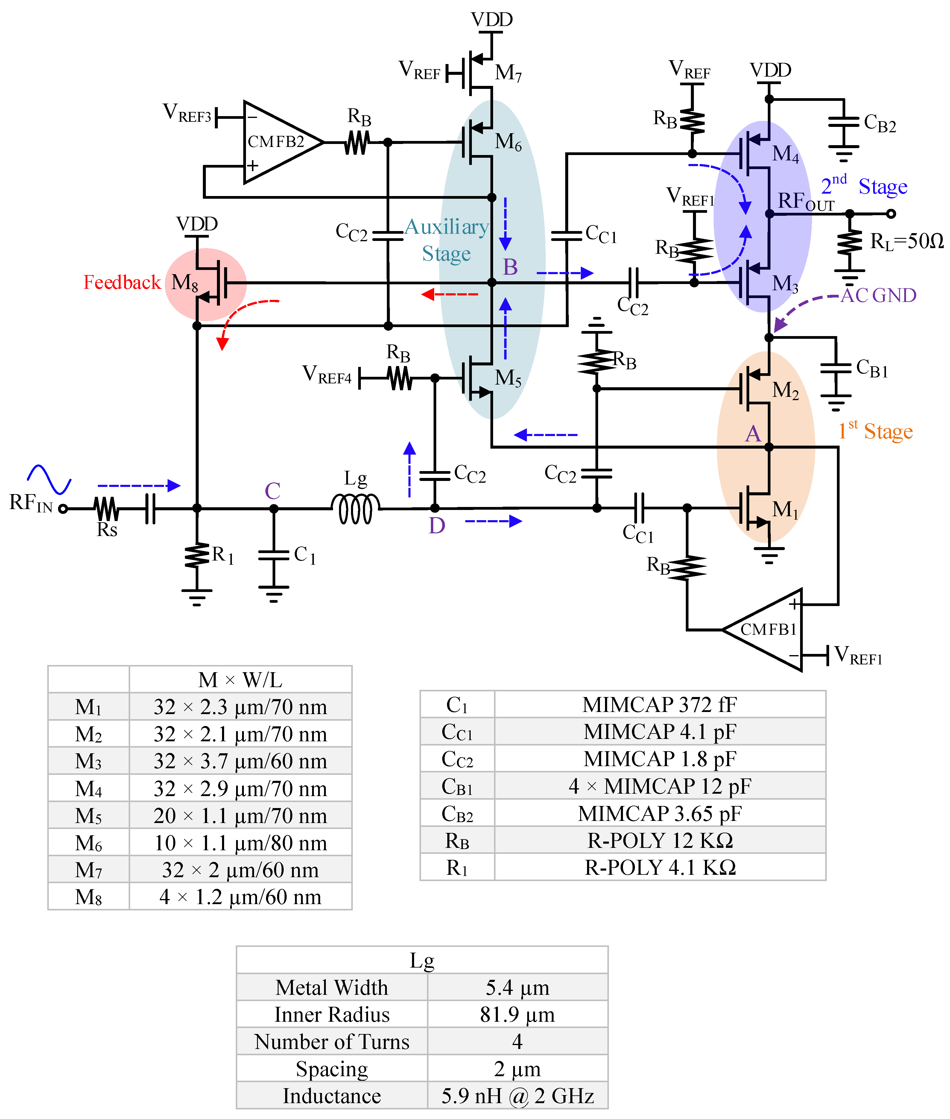
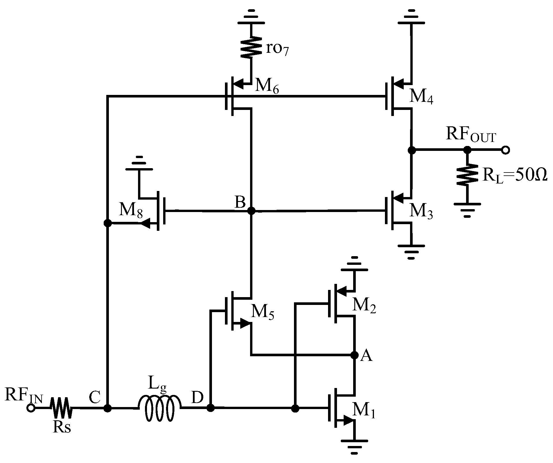
Figure 2 shows the schematic of the proposed wideband LNA with its component values. The proposed LNA consists of two stages. Transistors M1 and M2 form the first stage as a current-reuse circuit. The length of transistors M1 and M2 is chosen to be slightly longer than the minimum length of the used technology (65 nm) to increase the intrinsic impedance between source and drain (1/gds), which slightly increases the voltage gain at node A [17]. M1 and M2 also play the role of a gm-boosting for M5; therefore, the signal at node A is amplified by M5 and appears at node B. M5 and M6 are an auxiliary stage in the proposed LNA. M8 acts as shunt-series feedback to meet wideband input impedance matching and linearity improvement. M8 is biased in the sub-threshold region to decrease power. Also, since the gain at node B is high, input impedance matching is satisfied very well without increasing the feedback network coefficient (gm8). Transistors M3 and M4 form the second stage of the proposed LNA, which consumes the same DC current as the first stage and is decoupled from the first stage by capacitor CB1. The second stage also acts as a buffer stage, which is used to match the output impedance. The gate terminal of the M4 is also connected to the input (node C) and acts as a noise and distortion cancellation technique to improve the gain, NF, and linearity. This means that the noise and harmonic distortion returned by the feedback network are amplified by this transistor with a 180° phase difference and summed with the output, which reduces distortion and noise. Inductor Lg is used to achieve a flat gain, input impedance matching, and improved bandwidth. The Lg is a standard spiral-on-chip inductor which acts as a series inductive peaking element to compensate for parasitic capacitors (node D). The quality factor (Q-factor) of the Lg has a significant effect on the S21 and NF for frequencies above 1.5 GHz. Therefore, when the Q-factor decreases, S21 drops and the NF increases, resulting in the bandwidth reducing by −3 dB. The Q-factor of spiral inductors is influenced by the metal width and inner radius. Increasing the metal width reduces the series resistance, which enhances the Q-factor. However, it also increases parasitic capacitances, ultimately limiting the Q-factor at higher frequencies. On the other hand, a larger inner radius reduces both conductor losses and parasitic capacitance, leading to an improved quality factor [18]. To achieve optimal performance, the inductor geometry is carefully optimized for the highest possible Q-factor, as demonstrated in Figure 2. Additionally, temperature variations impact the Q-factor due to changes in metal resistivity and substrate losses. Specifically, as temperature decreases, the Q-factor increases slightly, though this effect is relatively minor [19].
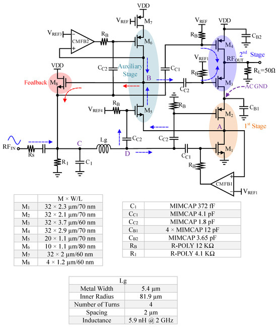
Figure 2.
Schematic of the proposed wideband LNA with its component values.
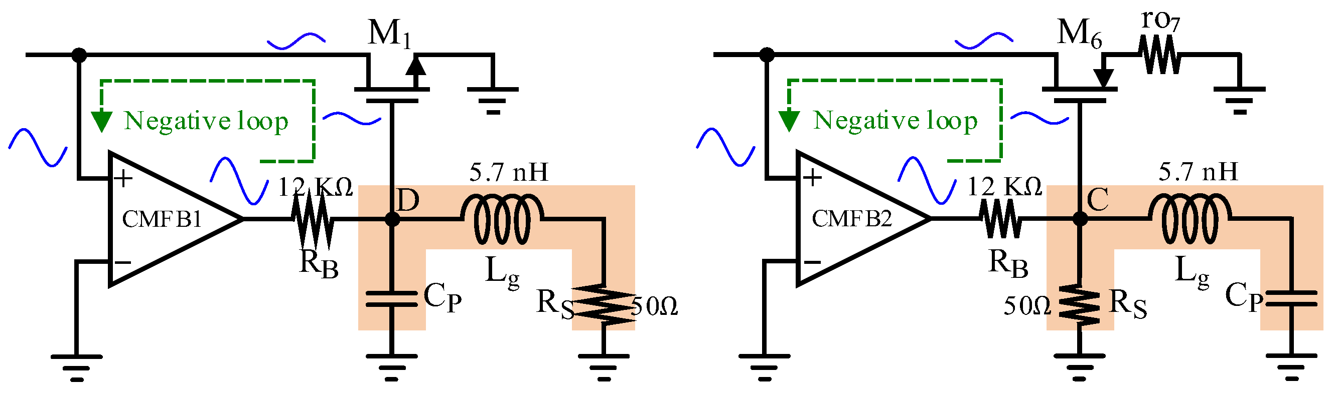
The DC points of nodes A and B are set by a common-mode feedback (CMFB) circuit. Although the combinations of CMFB with transistors M1 and M6 form a negative feedback loop, the effect of the CMFB loop on the proposed circuit has been investigated. Figure 3 shows the effect of CMFB1 and CMFB2 on the small signal response. The outputs of CMFB1 and CMFB2 are connected to the gates of M1 and M6, respectively, through a large resistor RB (12 KΩ). Since the impedance seen at these nodes (C and D) is approximately Rs (50 Ω), the return signal from the CMFB loop reaches the transistor gates with significant attenuation. Therefore, the CMFB loop does not affect the stability conditions of the proposed circuit. While a bypass capacitor could be used at the CMFB outputs to ensure stability at higher frequencies, it is not required in the proposed design.
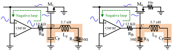
Figure 3.
Small-signal stability analysis of the feedback loop employing CMFB1 and CMFB2.
The details of the input impedance matching, voltage gain, NF, and linearity of the proposed single-ended wideband LNA are presented in the following section.
2.1. Input Impedance Matching
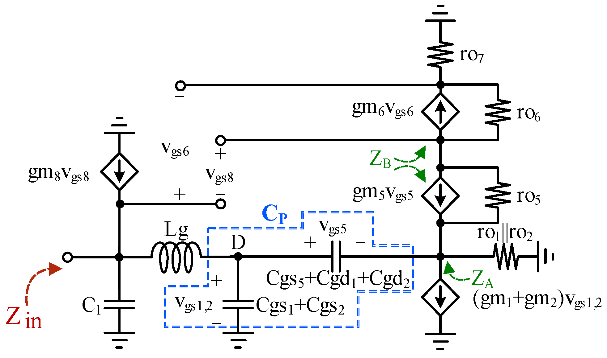
Figure 4 shows the small-signal model of the first stage for the input impedance calculation. The Lg compensates for the parasitic capacitors (CP) at node D for frequencies above 1.5 GHz. Using the Lg enables input impedance matching over the entire bandwidth (0.17 to 2.68 GHz).

Figure 4.
Small-signal model of the first stage for input impedance calculation.
As shown in Figure 4, the input impedance of the proposed LNA is approximately calculated as follows:
where , , and CP represents the parasitic capacitance at node D, which is approximately equal to
Based on Equation (1), when the Lg and CP are in resonance, the input impedance decreases significantly, which noticeably affects S11. However, the resonance frequency occurs at approximately 6 GHz, which is well beyond the desired bandwidth (0.17–2.68 GHz).
2.2. Voltage Gain
Figure 5 shows the AC model of the proposed LNA. M1 and M2 form the first stage, M5 and M6 constitute the auxiliary stage, and M8 forms the feedback network. Transistors M3 and M4 form the second stage.

Figure 5.
AC model of the proposed LNA.
Considering an output load RL of 50 Ω, the voltage gain can be approximately calculated as follows:
where . The Lg and parasitic capacitors are not considered in Equation (3) to simplify calculation and improve understanding; however, the effect of the Lg on the gain is explained below.
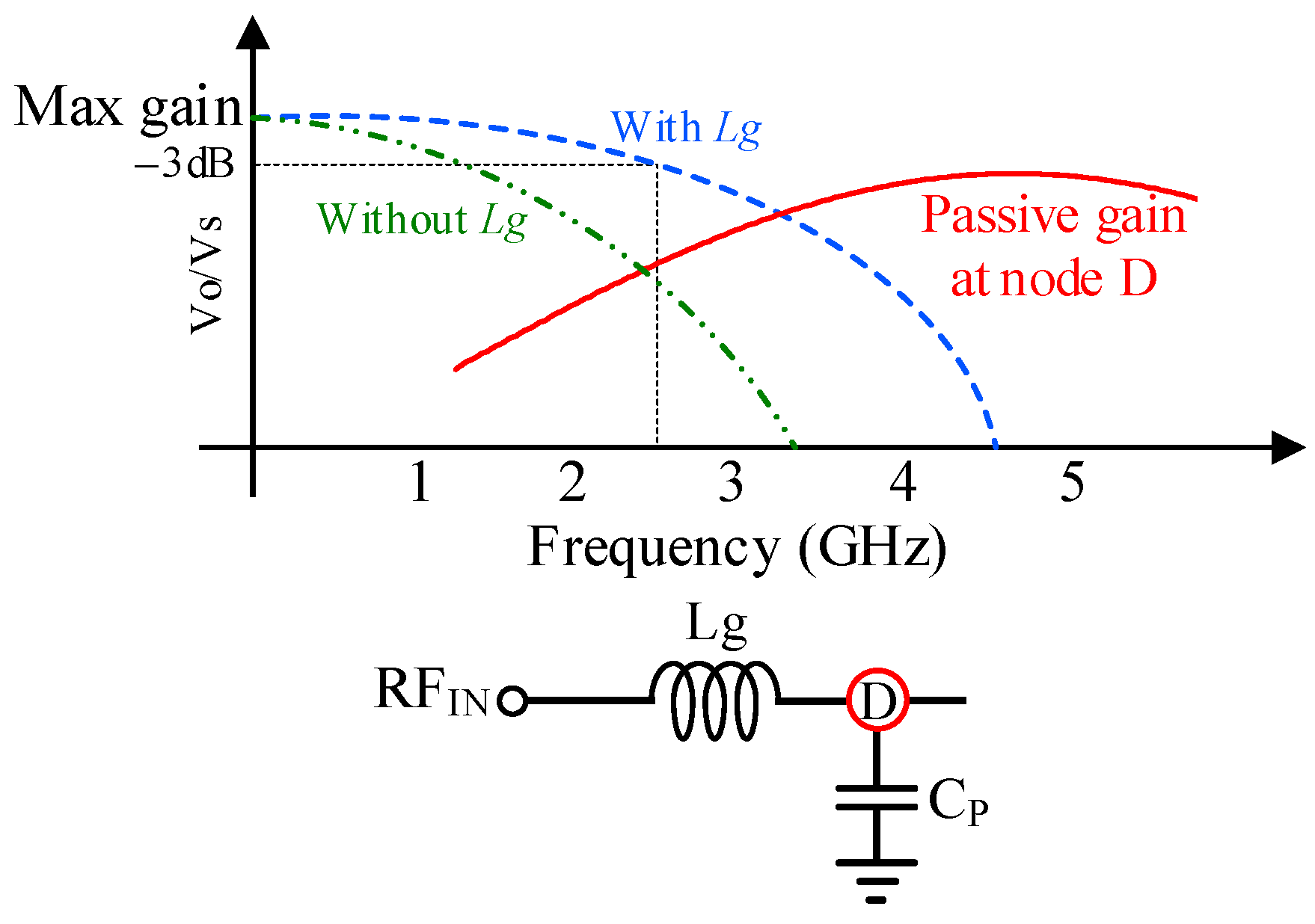
The Lg acts as a series inductive peaking element to compensate for the parasitic capacitances at node D. Figure 6 shows −3 dB bandwidth enhancement using the Lg as a series inductive peaking element. As shown, it is clear that before the current-reuse stage, passive gain is created by the Lg at node D, which increases the −3dB bandwidth.
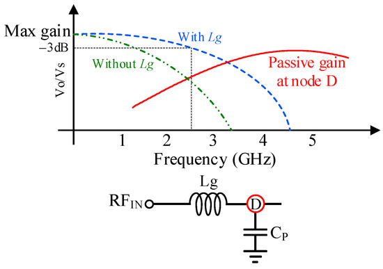
Figure 6.
Diagram of −3 dB bandwidth enhancement using the Lg as a series inductive peaking element.
2.3. Noise Analysis
Considering the proposed circuit consists of two stages, according to the Friis equation, it is clear that the first stage has the main effect on NF [2]. In the proposed LNA, the current-reuse circuit (M1, M2) dominates the thermal noise contribution. In the auxiliary stage, the thermal noise of M5 and M6 can be ignored due to their source-degenerated impedance [2]. In the feedback network, M8 is biased in sub-threshold region, where shot noise is comparable to thermal noise [20]. Although M8 injects noise into the circuit before the first stage which could affect the NF of entire receiver due to its equal amplification with the desired signal, this noise can be also ignored, because the impedance at the input node (node C) is sufficiently small. In the second stage, M4 is connected between the input and output as a CS stage serving as a noise cancellation technique [7]. Therefore, the dominant noise (M1, M2) can be cancelled by M4. The noise of M1 and M2 appears at the output, as described by Equation (4).
where , , and .
Therefore, complete noise cancellation is achieved when Equation (5) is satisfied, as derived from Equation (4).
In Equation (5), the value of gm4 is limited by low-power design constraints, preventing complete cancellation conditions from being met. Consequently, the NF is slightly improved. The resulting NF of the proposed circuit is calculated as follows:
where γ is the correction factor that is assumed identical for both the NMOS (M1) and PMOS (M2) transistors for simplicity. According to Equation (6), since the value of is significantly greater than 1, Equation (6) can be simplified to Equation (7).
As Equation (7) demonstrates, a stronger feedback network of M8 results in poorer NF performance. Furthermore, Equation (1) indicates that input impedance depends on feedback of M8, establishing a fundamental trade-off between S11 and NF.
2.4. Linearity Analysis
Typically, both single-ended and differential LNAs are implemented as single-stage designs to optimize linearity. For non-ideal amplifiers, the signal amplification can be approximated as follows [2]:
where α1 is the small-signal gain. In differential LNAs, due to the output differential signal, the second term of Equation (8) can be decreased significantly [2], but third-order harmonic is still problematic [8].
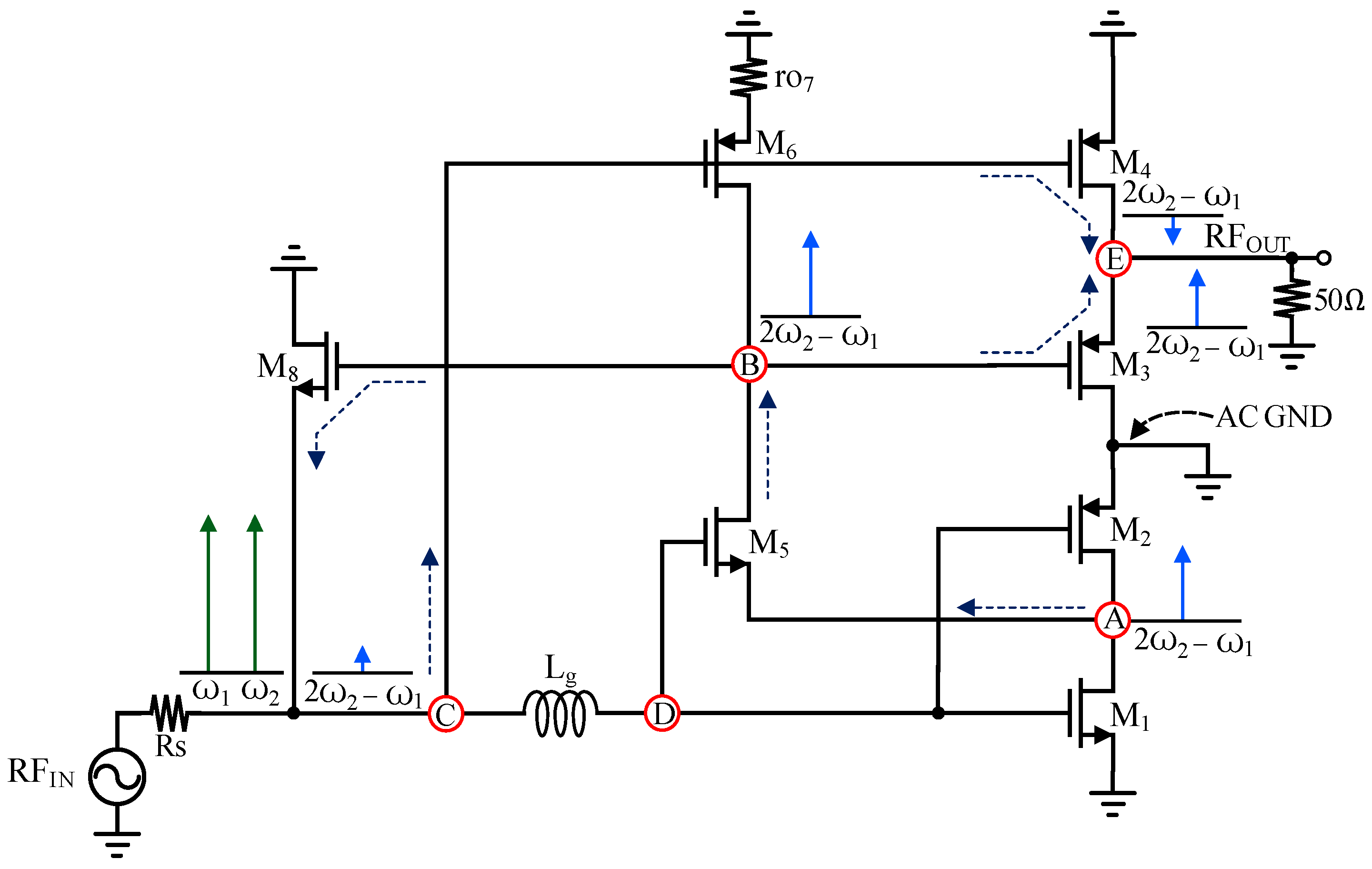
Figure 7 illustrates the mechanism of linearity improvement in the proposed circuit. when two interferer signals of are applied to the input, a third-order harmonic of and is generated at the output of the first stage (node A). The harmonic generated at node A appears at node B through M5 while being returned to the input (node C) via the feedback of M8. This feedback signal is then amplified by M4 with a 180° phase difference, thus reducing output distortion and improving linearity [7]. Similar to the noise analysis section, Equation (5) is also valid for canceling the generated harmonic, but as mentioned in the noise analysis, the generated harmonic cannot be cancelled completely. In the other words, the harmonics at node B reach node C with a large attenuation coefficient, which transistor M4 cannot fully compensate for due to its low-power design and consequently low gm4; this results in the linearity of the proposed LNA being improved by slightly less than 2 dB.
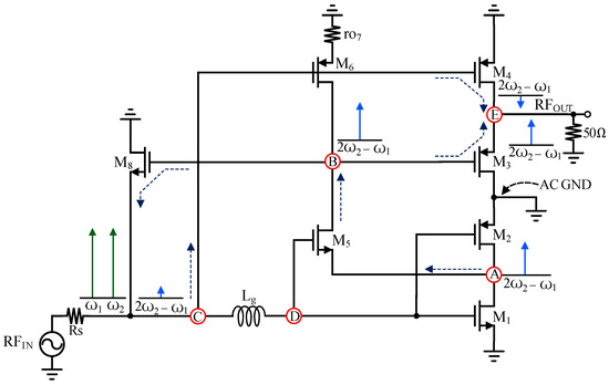
Figure 7.
The mechanism of linearity improvement.
3. Simulation Results
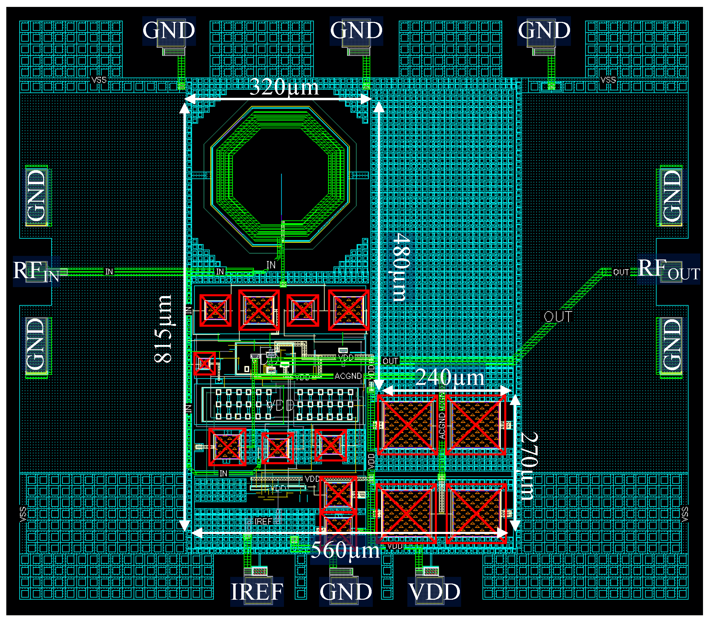
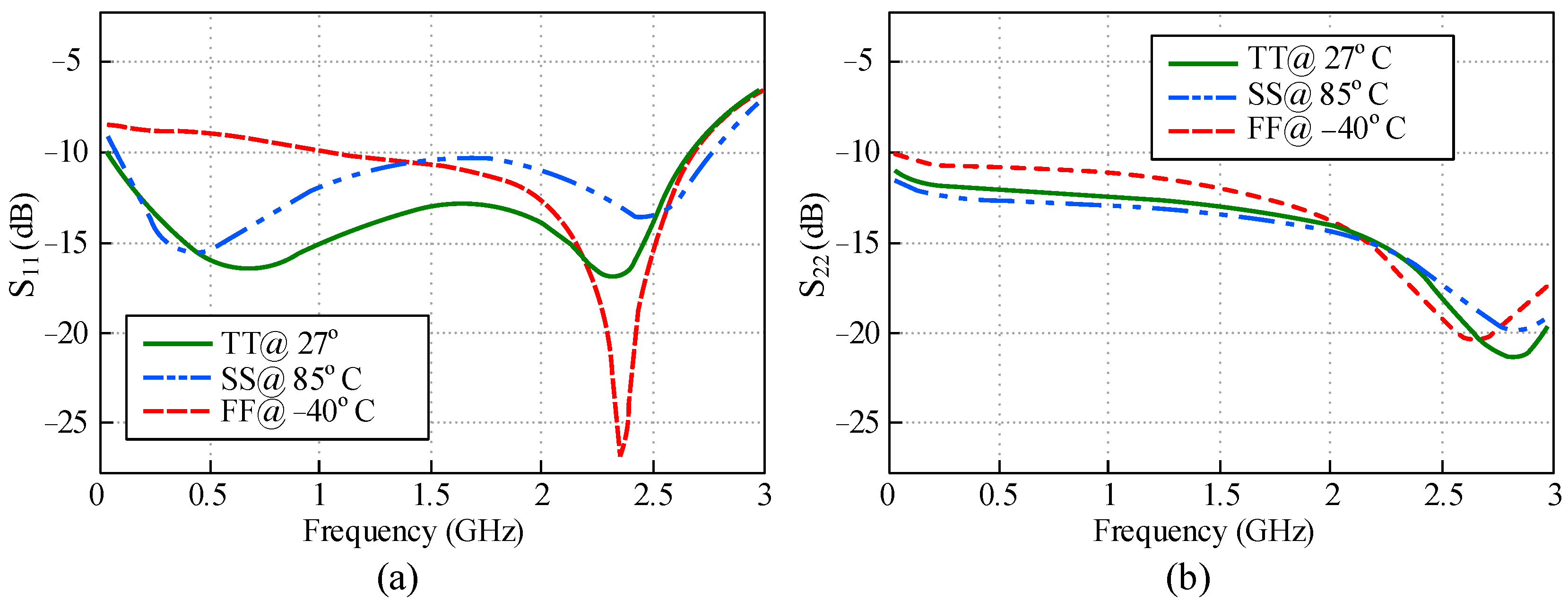
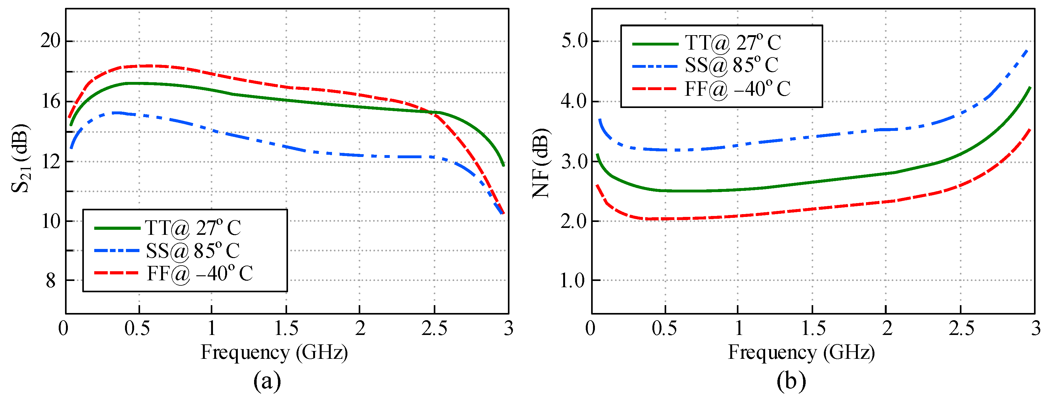
The proposed low-power single-ended wideband LNA is suitable for low-power multi-standard receivers that cover the frequency range of 0.17–2.68 GHz, including (GSM, WLAN and Bluetooth). The proposed LNA is designed in 65 nm CMOS technology with a 1 V supply voltage and is simulated using Cadence Spectre-RF. An external reference current (IREF) of 50µA is applied to the proposed circuit for biasing. Figure 8 shows the layout of the proposed wideband LNA with a core area of 0.3 mm2. The area of the proposed LNA including pads is 0.45 mm2. The post-layout simulation results of input return loss (S11), output return loss (S22), power gain (S21), and NF for the proposed wideband LNA across PVT and corner variations are presented in Figure 9 and Figure 10, respectively. Corner simulations are considered for the worst-case scenario (Fast–Fast (FF) at −40° and Slow–Slow (SS) at 85 °C) [8]. As shown in Figure 9 and Figure 10, both S11 and S22 remain below −10 dB; furthermore, S21 exceeds 15 dB, while the NF remains below 3.24 dB over the desired bandwidth. Based on Figure 9a, in FF mode at −40 °C, S11 shows a significant deviation from other conditions. This is because in CMOS technology, as the temperature decreases, the threshold voltage increases [21]. Therefore, with decreasing temperature, the voltage at node A increases while the current through M5 decreases significantly, causing a reduction in gm5. Based on Equation (1), the decreased gm5 reduces the feedback network loop effect, resulting in increased input impedance and S11.
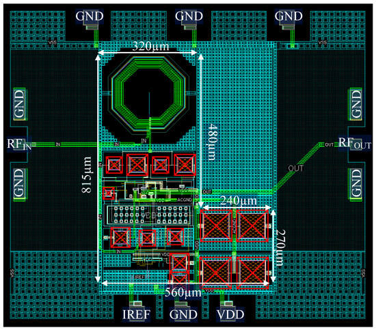
Figure 8.
The layout of the proposed wideband LNA.
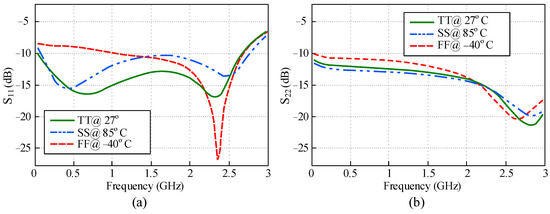
Figure 9.
Post-layout simulation results across temperature and corner variations of (a) S11 and (b) S22.
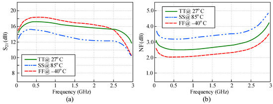
Figure 10.
Post-layout simulation results across temperature and corner variations of (a) S21 and (b) NF.
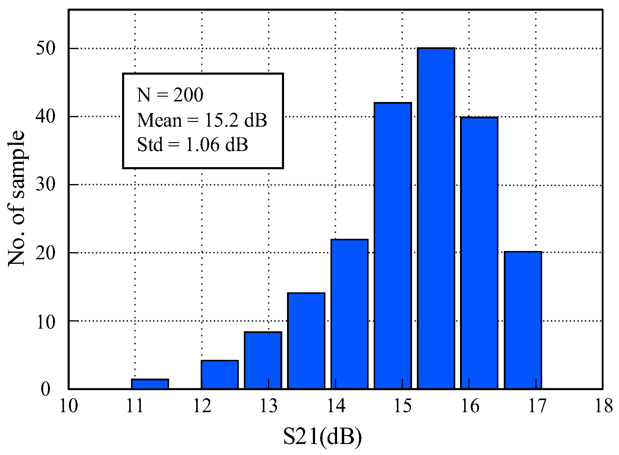
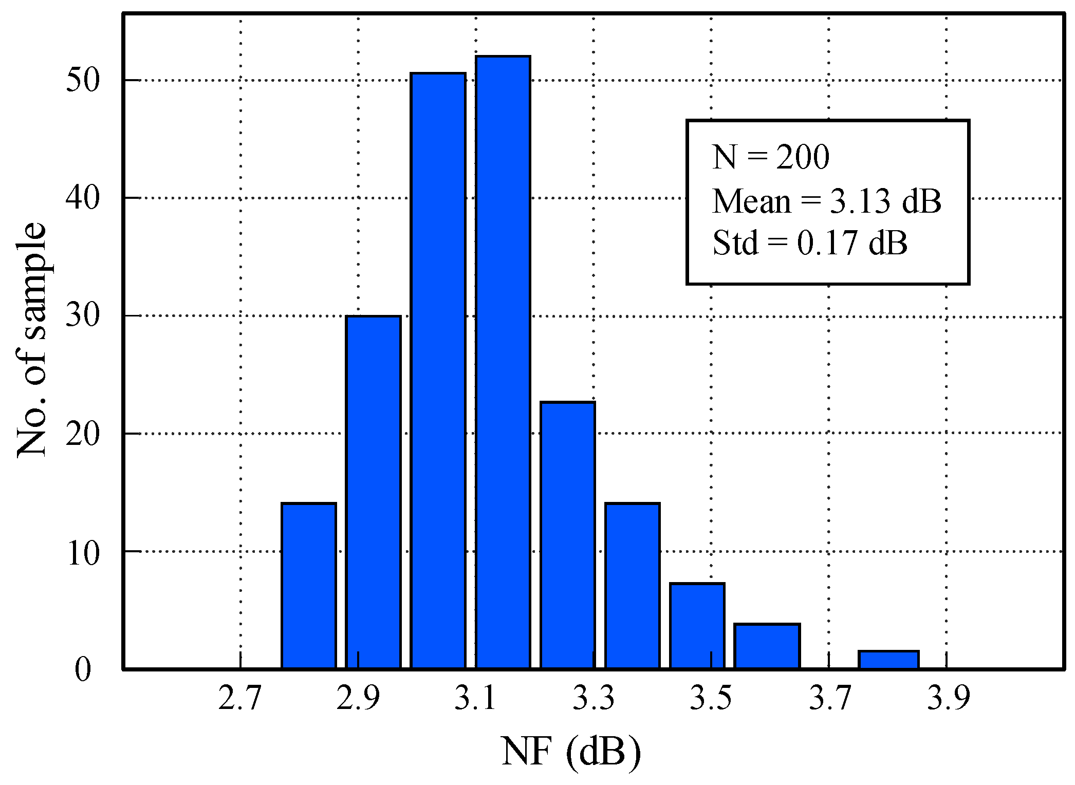
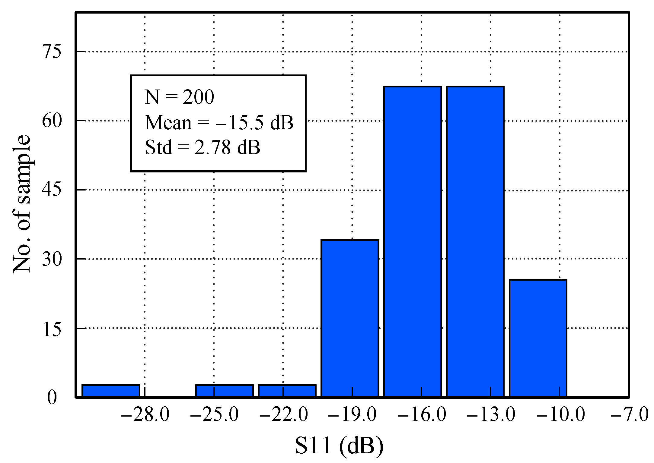
To validate the simulation results, Monte Carlo simulations were also conducted for S11, S21, and NF at sensitive frequency points, as shown in Figure 11, Figure 12 and Figure 13. Based on Figure 9 and Figure 10, since S11 in FF mode at −40 °C shows deviation in the sub-GHz range and S21 and NF can exhibit significant variations due to the Q-factor of the Lg above 2 GHz, the sensitive frequency points were selected as 500 MHz for S11 and 2.5 GHz for S21 and NF. As shown in Figure 11, Figure 12 and Figure 13, S21 and NF have average values of 15.2 dB and 3.13 dB at 2.5 GHz, respectively, and the mean S11 value at 500 MHz is −15.2 dB.

Figure 11.
Monte Carlo simulation results for S21 performance at 2.5 GHz.

Figure 12.
Monte Carlo simulation results for NF performance at 2.5 GHz.

Figure 13.
Monte Carlo simulation results for S11 performance at 500 MHz.
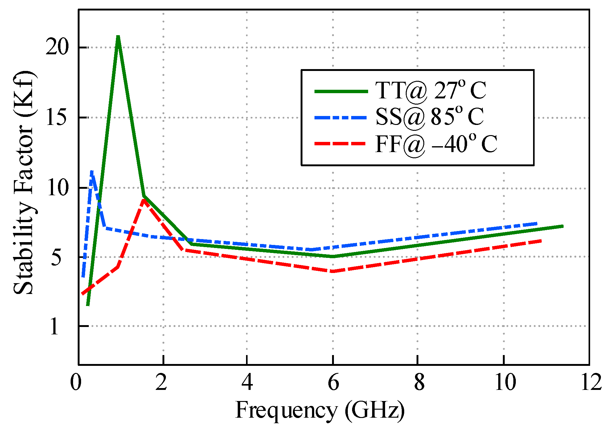
Figure 14 shows the stability factor (Kf) across process corners and temperature variations from 0.1 to 12 GHz. The stability factor exceeds unity across the entire 0.1–12 GHz range, demonstrating that the proposed circuit is unconditionally stable.
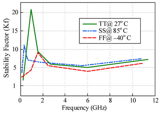
Figure 14.
Stability factor (Kf) across process corners and temperature variations (0.1 to 12 GHz).
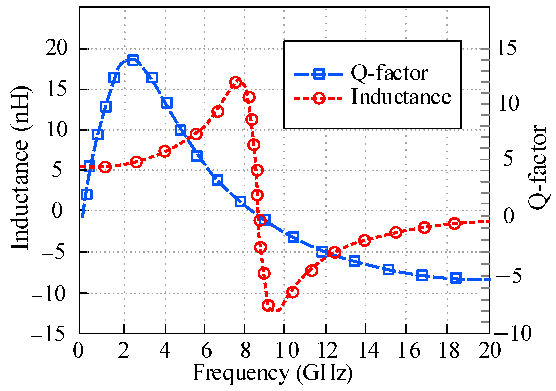
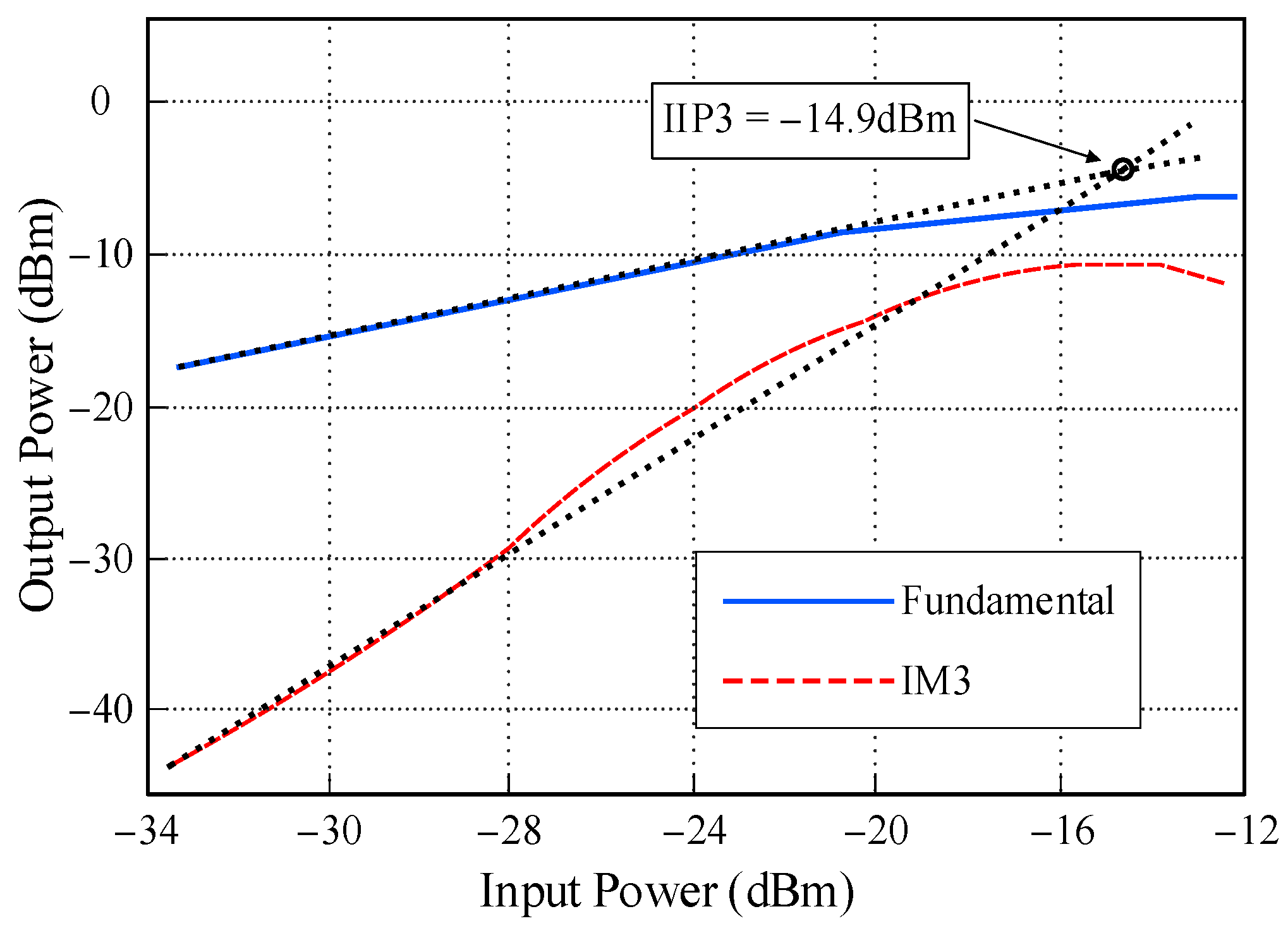
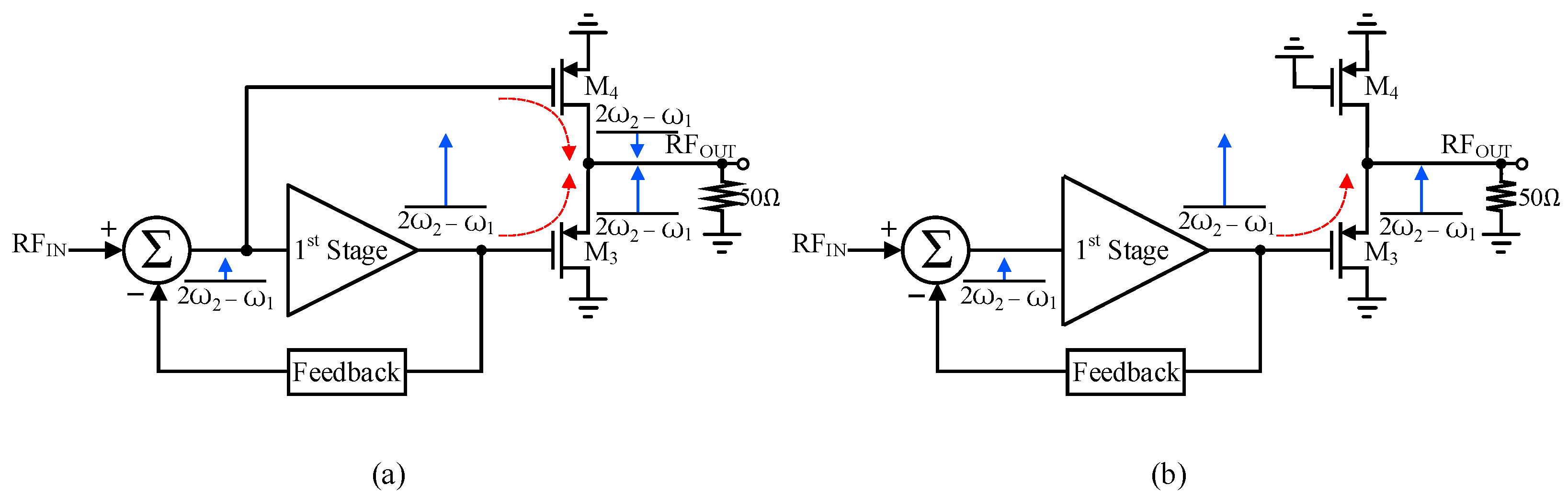
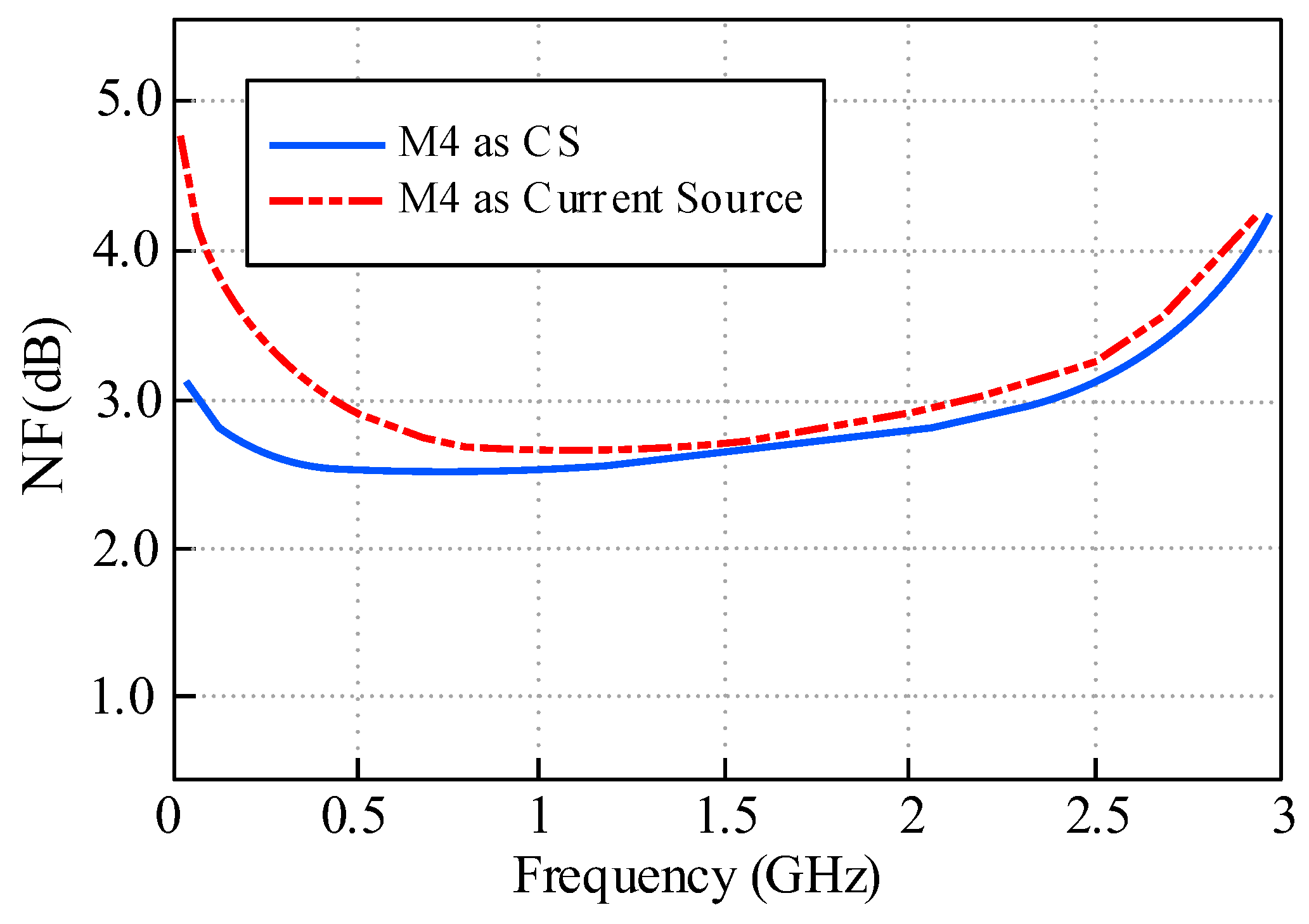
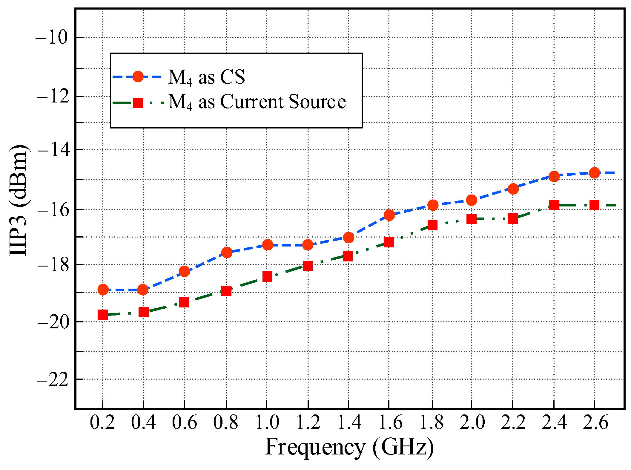
To verify the inductance and Q-factor of the Lg, electromagnetic (EM) simulation was performed using the Advance Design System (ADS) Momentum EM simulator. As depicted in Figure 15, the simulation results at 2 GHz indicate that Lg exhibits an inductance of 5.9 nH and a Q-factor of 13.9. The self-resonant frequency (SRF) occurs at approximately 9 GHz, well beyond the target operation bandwidth (0.17 to 2.68 GHz). Two-tone tests with 10 MHz spacing were performed at 2.4 GHz, and as shown in Figure 16, an intercept point three (IIP3) of −14.9 dBm was obtained. As mentioned in the noise and linearity analysis section, M4 improves both NF and linearity. To verify this, NF and IIP3 were simulated under two conditions, as illustrated in Figure 17a,b. The first case involves connecting the gate terminal of M4 to the input, where M4 operates as a CS amplifier, implementing the noise and distortion cancellation mechanism. The second case considers M4 functioning solely as a current source for the second stage. Figure 18 compares the NF for both modes. Based on Equations (4) and (5) and simulation results, it is clear that when M4 is connected to the input, the noise voltage at the first stage output is decreased and the NF improves. The IIP3 across the entire bandwidth was also simulated using two-tone tests with 10 MHz spacing, both with and without M4. Figure 19 shows the IIP3 versus frequency. Similar to the NF analysis, IIP3 improves when M4 is included. Equation (5) can be also used for distortion cancellation since the harmonic produced at node A can be cancelled similarly to the noise generated at node A.
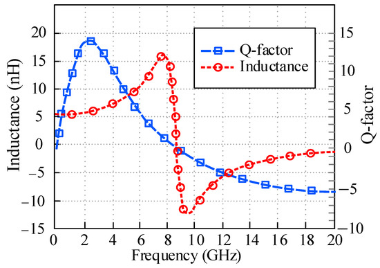
Figure 15.
Simulated inductance and Q-factor of the Lg from EM simulation.
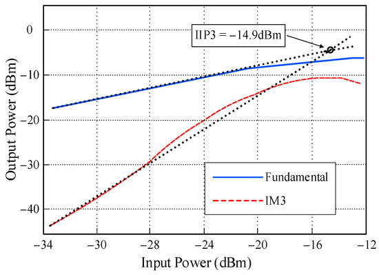
Figure 16.
The IIP3 at 2.4 GHz with 10 MHz spacing.
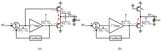
Figure 17.
M4 configurations: (a) CS circuit and (b) current source implementation.

Figure 18.
Comparison of NF between the two operating modes.
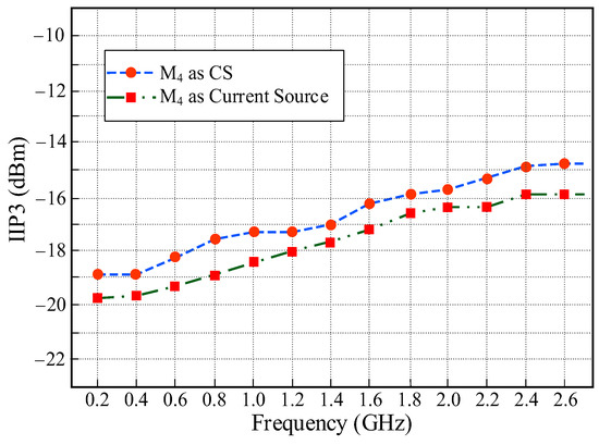
Figure 19.
IIP3 versus the input signal frequency with 10 MHz spacing for both modes.
Table 1 summarizes the performance results of the proposed wideband LNA across different corners and temperatures. Although the proposed LNA shows slight variations under different corner conditions, it demonstrates robust performance against both corner and temperature variations. Table 2 presents a comparison with state-of-the-art designs, benchmarking the proposed LNA against similar recent works. The Figure of Merit (FoM) is calculated as follows [15]:

Table 1.
Corners and temperature simulation results.
Table 2.
Performance comparison with several recent similar works.
Excluding [14], which achieves complete output impedance matching, other cited references have reported only the LNA core power consumption, resulting in higher FoM values than the proposed circuit. Only [11] includes the output buffer power of 9 mW, which would significantly reduce its FoM if properly accounted for. In comparison, the proposed LNA achieves output matching without requiring a buffer. Due to the combined circuits approach used in the proposed low-power design, the occupied die area is larger than other cited references. For example, two stages of the proposed circuit are isolated by large MIMCAPs. Although the proposed circuit occupies a large area, one advantage of the implemented topology is that it performs output impedance matching without requiring high power consumption.
4. Conclusions
In this paper, a low-power wideband single-ended LNA is analyzed. The proposed LNA covers frequency ranges from 0.17 to 2.68 GHz and is suitable for low-power multi-standards wireless applications. Two-stage amplifier implementation shares the same DC current bias and uses large MIMCAPs for isolation. A noise and distortion cancellation technique are employed to improve both NF and linearity. The circuit was simulated using Cadence Spectre-RF in 65 nm CMOS technology. Post-layout simulation results demonstrate acceptable performance with low power consumption, validating the theoretical analysis. Furthermore, the proposed LNA achieves full output matching without requiring an additional buffer, thereby reducing overall power consumption and making it particularly suitable for low-power applications.
Author Contributions
Conceptualization, F.S.B., M.N. and Y.K.S.; Validation: M.N. and T.B.K. and Y.K.S.; Writing—Original Draft Preparation: F.S.B.; Writing—Review and Editing: F.S.B., M.N., T.B.K. and Y.K.S.; Supervision: Y.K.S. All authors have read and agreed to the published version of the manuscript.
Funding
This research received no external funding.
Institutional Review Board Statement
Not applicable.
Informed Consent Statement
Not applicable.
Data Availability Statement
Data are contained within the article.
Conflicts of Interest
The authors declare no conflicts of interest.
References
- Wan, Q.; Liu, J.; Chen, S. An Inductorless Gain-Controllable Wideband LNA Based on CCCIIs. Micromachines 2022, 13, 1832. [Google Scholar] [CrossRef] [PubMed]
- Razavi, B. RF Microelectronics; Prentice Hall: New York, NY, USA, 2012; Volume 2. [Google Scholar]
- Mir-Moghtadaei, S.V.; Bidabadi, F.S. A CMOS 3.5 GHz Bandwidth Low Noise Amplifier using Active Inductor. AUT J. Electr. Eng. 2025, in press. [Google Scholar]
- Hu, B.; Yu, X.P.; Lim, W.M.; Yeo, K.S. Analysis and Design of Ultra-Wideband Low-Noise Amplifier with Input/Output Bandwidth Optimization and Single-Ended/Differential-Input Reconfigurability. IEEE Trans. Ind. Electron. 2014, 61, 5672–5680. [Google Scholar]
- Farshad, S.B.; Mir-Moghtadaei, S.V. An Ultra-Wideband 0.1–6.1 GHz Low Noise Amplifier in 180 nm CMOS Technology. J. Circuits Syst. Comput. 2020, 30, 2150104. [Google Scholar]
- Cheng, K.-W.; Chen, W.-W.; Yang, S.-D. A Low Power Sub-GHz Wideband LNA Employing Current-Reuse and Device-Reuse Positive Shunt-Feedback Technique. IEEE Microw. Wirel. Compon. Lett. 2022, 32, 1455–1458. [Google Scholar] [CrossRef]
- Bruccoleri, F.; Klumperink, E.A.M.; Nauta, B. Wide-band CMOS low-noise amplifier exploiting thermal noise canceling. IEEE J. Solid-State Circuits 2004, 39, 275–282. [Google Scholar] [CrossRef]
- Shirmohammadi, B.; Yavari, M. A Linear Wideband CMOS Balun-LNA With Balanced Loads. IEEE Trans. Circuits Syst. II Express Briefs 2021, 69, 754–758. [Google Scholar] [CrossRef]
- Kim, S.; Kwon, K. A 50-MHz-1-GHz 2.3-dB NF noise- cancelling balun-LNA employing a modified current-bleeding technique and balanced loads. IEEE Trans. Circuits Syst. I 2019, 66, 546–554. [Google Scholar] [CrossRef]
- Kim, S.; Kwon, K. Broadband balun-LNA employing local feedback gm-boosting technique and balanced loads for low-power low-voltage applications. IEEE Trans. Circuits Syst. I 2020, 67, 4631–4640. [Google Scholar]
- Tiwari, S.; Mukherjee, J. An inductor less wideband Gm-boosted balun LNA with NMOS-PMOS configuration and capacitively coupled loads for sub-GHz IoT applications. IEEE Trans. Circuits Syst. II 2021. early access. [Google Scholar]
- Kishore, K.H.; Venkataramani, B.; Sanjay, R.; Rajan, V.S. High gain inductor less wideband Balun-LNA using asymmetric CCC & BIST using RMS detectors. AEU-Int. J. Electron. Commun. 2019, 105, 135–144. [Google Scholar]
- Mahmood, H.U.; Lee, S.-G.; Kim, J. A 0.1–4.2 GHz, 960-μW Inductor-Less and Negative Shunt Feedback LNA With Simultaneous Noise and Distortion Cancellation and Bandwidth Extension. IEEE Trans. Circuits Syst. I 2024, 71, 2563–2575. [Google Scholar] [CrossRef]
- Pu, Y.; Li, W.; Li, Q.; Ma, X.; Xu, H. A 0.2–3.2-GHz active Balun-LNA with 1.4–2.18-dB NF utilizing asymmetric current distribution in 28-nm CMOS. IEEE Microw. Wirel. Technol. Lett. 2025, 35, 326–329. [Google Scholar] [CrossRef]
- Liu, Z.; Boon, C.C.; Dong, Y. A 0.6 V, 1.74 mW, 2.9 dB NF Inductor less Wideband LNA in 28-nm CMOS Exploiting Noise Cancellation and Current Reuse. IEEE Trans. Circuits Syst. I 2024, 71, 3561–3572. [Google Scholar]
- Park, J.-W.; Kim, D.-Y.; Im, D. A Broadband Gm-Boosted Active Feedback CMOS Low-Noise Amplifier for Low- and Mid-Band 5G Applications. IEEE Trans. Circuits Syst. II Express Briefs 2025, 72, 399–403. [Google Scholar] [CrossRef]
- Hu, S.; Du, J.; Chen, P.; Nguyen, H.M.; Quinlan, P.; Siriburanon, T.; Staszewski, R.B. A Type-II Phase-Tracking receiver. IEEE J. Solid-State Circuits 2021, 56, 427–439. [Google Scholar] [CrossRef]
- Bahl, I.J. High-performance inductors. IEEE Trans. Microw. Theory Tech. 2001, 49, 654–664. [Google Scholar] [CrossRef]
- Hoen, T.J.; Jin, Y.; Annema, A.-J.; Wils, N.; Verlinden, J.; Nauta, B. Low TCL, High-Q Inductors in Standard CMOS. IEEE Microw. Wirel. Technol. Lett. 2024, 34, 179–182. [Google Scholar] [CrossRef]
- Sarpeshkar, R.; Delbruck, T.; Mead, C. White noise in MOS transistors and resistors. IEEE Circuits Devices Mag. 1993, 9, 23–29. [Google Scholar] [CrossRef]
- Filanovsky, I.M.; Allam, A. Mutual compensation of mobility and threshold voltage temperature effects with applications in CMOS circuits. IEEE Trans. Circuits Syst. I Fundam. Theory Appl. 2001, 48, 876–884. [Google Scholar] [CrossRef]
Disclaimer/Publisher’s Note: The statements, opinions and data contained in all publications are solely those of the individual author(s) and contributor(s) and not of MDPI and/or the editor(s). MDPI and/or the editor(s) disclaim responsibility for any injury to people or property resulting from any ideas, methods, instructions or products referred to in the content. |
© 2025 by the authors. Licensee MDPI, Basel, Switzerland. This article is an open access article distributed under the terms and conditions of the Creative Commons Attribution (CC BY) license (https://creativecommons.org/licenses/by/4.0/).