1. Introduction
Electronic devices are made up of multiple components, like resistors, capacitors, inductors, diodes, and transistors [
1]. They are designed to elaborate, transmit, or receive data, in order to perform a specific function such as communication, computation, and automation [
2]. These systems are used in numerous sectors, including consumer electronics, automotive, home automation, energy management, biomedical, and industrial applications.
In the energy sector, embedded electronics support distributed monitoring, load balancing, fault detection, and predictive maintenance of power infrastructures [
3,
4]. Electronic systems such as Smart Meters, Power Loggers, Sensors, Microcontroller, Gateways, Raspberry Pi, and Actuators have various applications to ensure the correct operation of the electrical grid [
5,
6,
7]. In fact, these systems improve grid reliability, allow achieving a balance between supply and demand, evaluate the effectiveness of demand management strategies, collect real-time energy consumption data, reduce energy costs, and provide utilities with the possibility to manage services more efficiently. In the healthcare sector, biomedical devices significantly contribute to diagnosis, treatment, and monitoring of various medical conditions, highlighting how the approach to medicine has become increasingly personalized and predictive [
8,
9]. These technologies are capable of improving quality of human life, monitoring patients’ vital parameters, and preventing risk situations through continuous physiological data processing [
10,
11]. Building on the importance of electronic devices in various settings, which are essential for reducing environmental impact and supporting daily human activities, their quality is an indispensable requirement in the design, production, and operation phases [
12,
13]. Despite the advantages these devices bring to their application sectors, it should be noted that human–technology interaction presents both positive and negative aspects [
14]. Drawbacks are mainly associated with device degradation over time, as they operate by absorbing electrical energy [
15]. The study [
16] highlighted that prolonged operation of devices can compromise the integrity of electronic components due to cyclic thermal stresses, affecting performance and safety. Component wear, voltage drops, or Joule-effect overheating significantly affect their safety. Additionally, the increasing complexity and miniaturization of these devices have introduced new challenges related to reliability, particularly concerning thermal management in high-density electronics systems, where uncontrolled thermal stress can lead to performance degradation, reduced lifespan, or complete failure of critical components. Among the main causes of thermal degradation are defects in PCBs, including microcracks, faulty solder joints, and inadequate thermal interfaces [
17]. Although these defects originate from manufacturing imperfections, they often emerge over time due to mechanical and environmental stresses [
18]. Since the reliability of devices is essential for safe human interaction, non-invasive monitoring methods are required. Moreover, device design and manufacturing must ensure maximum human protection under both normal and fault conditions [
19,
20,
21]. To this end, design processes increasingly rely on precise computational codes and a deep understanding of the physical properties of the device components, depending on the specific application use [
22,
23]. Electronic subsystems within biomedical devices must operate continuously and reliably under variable thermal and electrical conditions [
24,
25,
26]. Therefore, monitoring the quality of electronic devices over time is fundamental, considering that localized overheating within them can damage biological issues or cause system failures, both with severe consequences. For this purpose, non-invasive and highly accurate thermal monitoring methods are required to detect thermal anomalies and stress conditions promptly, especially during the initial operating phase.
Traditional monitoring methods often fail to detect such anomalies, especially in multilayer PCBs, where localized heating may not immediately manifest as surface temperature variations [
27]. Moreover, these methods are usually conducted offline, lack spatial resolution, and cannot provide continuous real-time diagnostics. Consequently, these imperfections may evolve into critical failures, limiting predictive maintenance and compromising human safety [
28]. Unlike traditional monitoring methods, often limited to simulations or surface measurements, IRT plays a key role not only in predictive maintenance but especially in quality control, enhancing the safety and efficiency of electronic systems. IRT has gained traction because it enables visualization of surface temperature distributions and real-time identification of thermal anomalies without interfering with device operation [
29,
30]. However, conventional thermographic analysis is affected by external variables such as noise, variable emissivity, and environmental disturbances.
Furthermore, as correct data interpretation still requires expert assessment, automation and scalability of this technique are severely limited. Recently, several AI-based approaches have achieved good results in the automatic classification of surface defects in PCBs. Although numerous studies have integrated IR thermography and neural networks for the detection of anomalies in PCBs [
31,
32,
33], none of them assess the effect of architectural parameters on segmentation quality in a statistically rigorous manner. Existing studies are generally limited to empirical optimisations without variance analysis or structured experimental planning [
34,
35,
36]. However, they mainly focus on obvious structural issues, while neglecting latent thermal ones. Several studies have attempted to address this gap. Refs. [
37,
38,
39] proposed an integrated system combining FEM modelling, IR thermography, and AI for monitoring thermal stress in biomedical device PCBs [
40]. Active thermography is used to identify hotspots indicative of voltage overloads or thermal anomalies during the operation of a medical device [
41,
42]. The acquired thermograms formed a diverse dataset of IR images, which was subsequently processed by AI algorithms to improve thermal stress area identification accuracy. AI-guided thermographic analysis proved effective in supporting the automatic localization and classification of thermal anomalies, real-time fault detection, and predictive maintenance strategies. Recent studies present models that combine infrared thermography, finite element method (FEM) simulations, and AI to detect thermal defects in the electronic boards of biomedical devices [
43,
44]. Thermal data were acquired both through passive (without external excitation) and active (with controlled electrical excitation) thermography [
45,
46,
47]. For automatic real-time classification of thermal anomalies, a Convolutional Neural Network (CNN) was implemented and optimized for low-resolution IR data processing [
48,
49]. The AI model was executed on a Raspberry Pi platform to analyse real-time thermal data and detect thermal anomalies. The system’s performance was validated through experimental measurements, revealing strong agreement between the predicted and observed thermal stress regions in terms of position and intensity [
50,
51]. The development of these hybrid methodologies arises from the need to overcome the limitations of isolated approaches in simulation and thermal anomaly segmentation using Machine Learning (ML). To fill the gap identified in the scientific literature, this study presents an integrated system combining IR thermography, AI, Taguchi Method, and ANOVA [
52,
53,
54]. The novelty of the proposed study lies in the use of Genichi Taguchi and Ronald Fisher techniques for the thermal stress control of a generic PCB.
While the segmentation-classification process is based on the methodological foundations introduced in [
16], the present study extends it by explicitly addressing the constraints of real-time monitoring. In particular, this study introduces temporal thermographic analysis, statistical optimisation of inference efficiency through Taguchi–ANOVA, and implementation-oriented evaluation aimed at integrated platforms. These aspects, which were not addressed in our study [
16], represent the main innovative contributions of this paper.
Unlike current models, which are based solely on end-to-end CNNs, the proposed pipeline combines U-Net segmentation, physical thermal descriptors, and MLP classification, providing a higher level of interpretability based on thermodynamic principles. The IR acquisitions form a dataset for specialized AI model training, which combines thermal anomalies segmentation using U-Net with a MLP classifier for heat distribution patterns. AI is employed in this paper to improve the accuracy of identifying areas under thermal stress during the operation of the PCB. Subsequently, for the application of the statistical methods chosen in this study, four hyperparameters of the U-Net model are selected: Parameters, FLOPs, Inference Time, and Time per Image. Preliminary sensitivity analysis showed that architectural parameters such as batch size or filter count produced less than 1% variation in
F1-score and were therefore excluded from the Taguchi study. The Taguchi method determines the optimal configuration of the selected factors, while ANOVA evaluates the effect of each factor on the
F1-score response. The proposed integrated system not only offers more accurate detection and classification of thermal anomalies, but also allows for the statistical validation of AI performance. The joint use of Taguchi and ANOVA makes it possible to quantify, with statistical rigour, the individual contribution of the hyper-parameters, highlighting those that are truly significant and drastically reducing the number of experiments required by conventional methods such as grid search and random search. The study is structured as follows:
Section 2 explains the applications of PCBs and Non-Destructive Testing (NDT) importance in their thermal stress control.
Section 3 presents the measurement campaign using a FLIR P660 infrared camera and parametric methods Taguchi–ANOVA.
Section 4 illustrates results and discussion, focused on AI algorithms and the statistical techniques proposed. Finally, conclusions and future developments are presented.
4. Results
To detect the thermal radiation naturally emitted by a generic PCB during its normal operation, a FLIR P660 model thermal camera was used. The main technical specifications of the FLIR P660 are listed in
Table 6.
These specifications make the FLIR P660 suitable for detecting subtle temperature gradients in electronic boards, where thermal anomalies can manifest with variations of less than 1 °C. The measurement campaign presented in this work was conducted in accordance with UNI-EN-16714:2016 [
86]. Before acquiring the thermal images, the instrument configuration was adapted to the operating environment, with appropriate balancing of the following parameters:
- •
Emissivity, ε = 0.92;
- •
Operator position: the FLIR P660 thermal camera was positioned approximately 0.3 m away from the electronic board to reduce angular effects on the emissivity measurement;
- •
Ambient outdoor temperature and humidity from the sector: the environment was kept thermally stable, with an ambient temperature of 22 °C and a relative humidity of 50%;
- •
Temperature reflected on the thermal camera: an object does not emit only infrared radiation but also reflects that coming from the surrounding environment. If this value is not set correctly, the thermal camera can overestimate or underestimate the object’s temperature distribution, distorting the conclusions of the thermographic analysis.
The absence of unwanted thermal reflections, the correct emissivity setting, and environmental stability ensure the reliability of the acquired information and its usability in a diagnostic context.
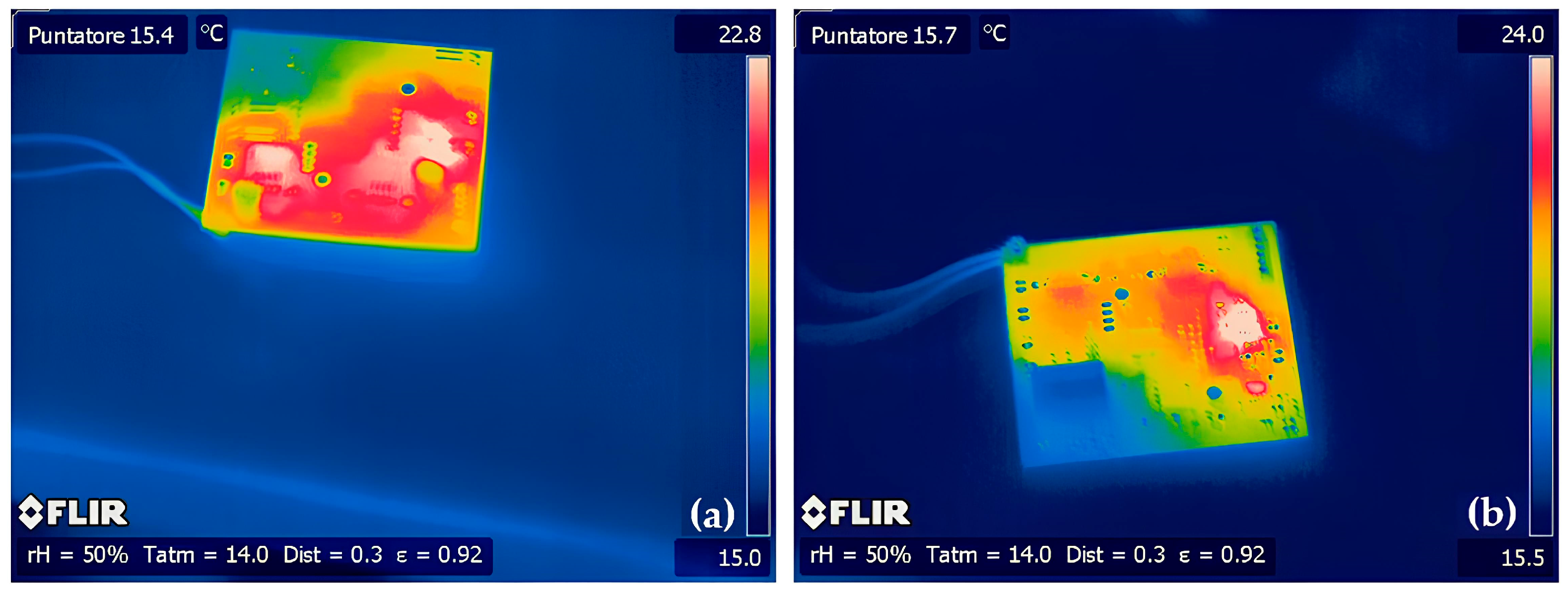
Figure 2 represents the initial phase of the experimental campaign for thermal image acquisition, conducted on a generic PCB.
Figure 2 shows the operational setup prepared at the NDT laboratory of the Mediterranean University of Reggio Calabria, where the experimental infrastructure for identifying thermal anomalies in the PCB was established. The measurement campaign involved acquiring video sequences in SEQ format, recorded at a sampling frequency of 30 Hz for a total time of 60 s. Additional tests conducted on desktop GPU-based systems showed marginal accuracy improvements but no proportional gain in temporal resolution, confirming that the Raspberry Pi platform represents an optimal trade-off between performance and deployment feasibility for real-time applications.
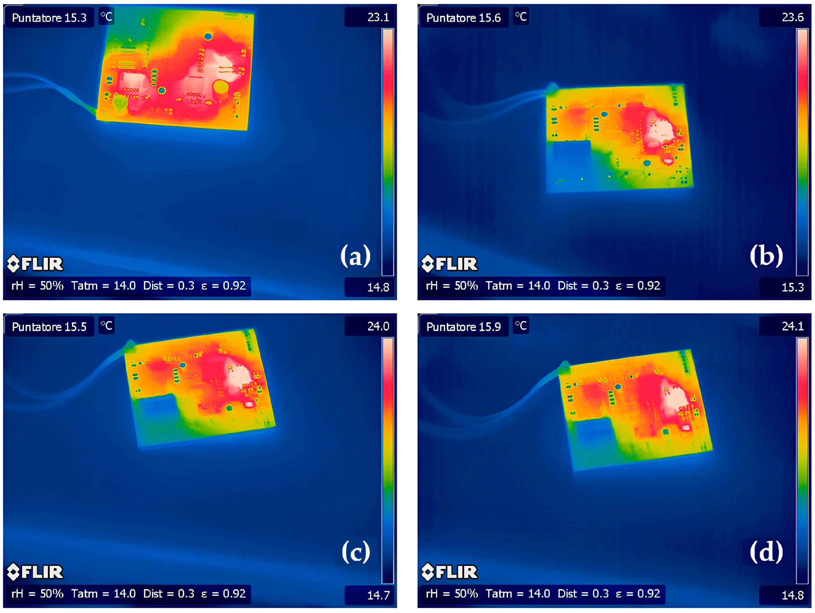
Figure 3 shows the real-time thermal images acquired during the PCB’s operation, which allow for the analysis of key characteristics such as heat generation and dissipation, as well as gradients and possible thermal anomalies. The thermograms reported in
Figure 3 were extracted from a continuous acquisition stream at 30 Hz, corresponding to a temporal resolution of 33 ms per frame. This enables the monitoring of fast thermal transients that are typically missed by offline or snapshot-based thermographic inspections. Considering the optimized inference time of 27.15 ms per image, the proposed system is capable of near-continuous real-time analysis without frame loss, representing an efficiency improvement of approximately one order of magnitude compared to traditional post-processing-based thermographic workflows.
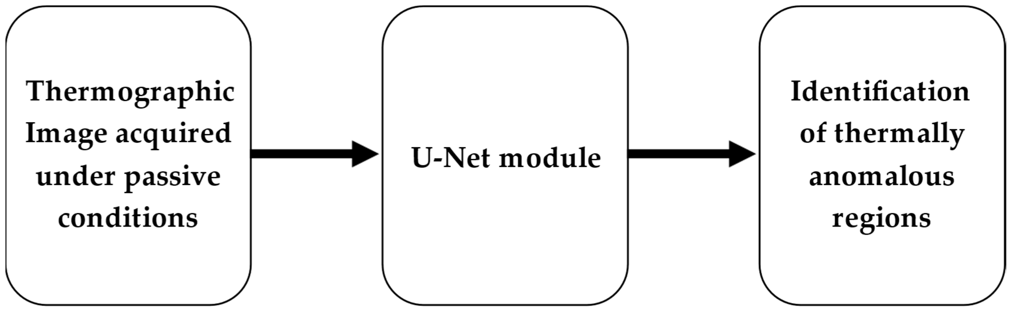
The thermograms, acquired according to the principles of the UNI-EN-16714 standard, were used as input for training intelligent segmentation and classification algorithms. The approach integrates Deep Learning with physically inspired feature extraction and Machine Learning classification. For the automatic and real-time identification of thermal anomalies in the PCB, the supervised image segmentation model U-Net was employed. The Deep Learning model processes the acquired thermograms, producing a binary mask where each pixel of the original IR image can be labelled as:
- •
Thermally anomalous area (value 1);
- •
Thermally normal area (value 0);
Figure 4 schematically shows the segmentation process.
Subsequently, through thermal diffusion analysis, the heat propagation within the PCB is mathematically described. A series of physical quantities, known as descriptors, have been calculated and are grouped into a feature vector F (17).
Note that each thermal image is converted into a vector of numerical features. These vectors were used as input for the heat diffusion model classification algorithm.
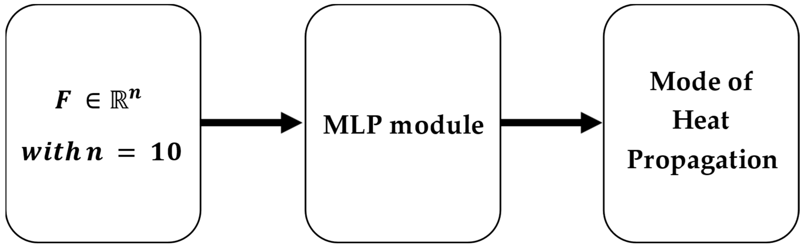
To distinguish between the different modes of heat transfer, a Multi-Layer Perceptron (MLP) classifier was employed. This Machine Learning algorithm is capable of recognizing four distinct categories of thermal diffusion: Localized Hotspot, Diffused Anomaly, Asymmetric Propagation, and Uniform Heating. A schematic representation of the classification process is presented below (
Figure 5).
AI-based thermographic analysis allowed for the detection of hotspots near defective PCB components, but most importantly, the development of localized heating at a critical component, where surface temperatures peaked at approximately 127 °C. The thermal peak of approximately 127 °C is consistent with typical overheating patterns observed in power regulators and microcontrollers under load, confirming that the method highlights physically plausible heat sources. Taguchi and ANOVA techniques were employed to statistically confirm the performance of the U-Net segmentation module. These techniques allow for a systematic analysis of the influence of the selected hyperparameters on the quality of binary segmentation, contributing to strengthening the reliability of the AI algorithm proposed by [
16].
The first phase of the Taguchi method involves appropriately selecting the hyperparameters of the U-Net model and their levels (
Table 7).
The three levels for each hyperparameter were selected based on preliminary feasibility tests and represent low, medium, and high computational loads compatible with real-time deployment. This choice aligns with Taguchi design principles, which recommend a limited number of levels to balance experimental efficiency and statistical significance.
The following is a description of the hyperparameters listed in
Table 7:
- •
Parameters represent the size of the model in terms of learnable weights, generally in the millions. In the U-Net model, the number of parameters primarily increases with the depth of the architecture, meaning the number of encoding and decoding levels, and with the introduction of additional layers, such as 3 × 3 convolutions. A greater number of parameters can improve the model’s ability to accurately locate thermal anomalies in PCBs. However, it also leads to an increase in the memory required by the model to perform tasks;
- •
FLOPs (Floating Point Operations) indicate the number of floating-point operations the model needs to perform to process a single image, expressed in Giga FLOPs or GFLOPs. The operations to be performed are generally in the billions. In the U-Net architecture, this factor depends on the resolution of the IR images, kernel sizes, and additional operations, including downsampling, upsampling, skip connections, regularization, and concatenations. FLOPS represent a theoretical indicator of computational complexity that is independent of hardware. Typically, a higher FLOPs value results in a longer computation time. However, the actual execution time depends on the mapping efficiency and model optimization;
- •
Time per Image, also known as image processing time, is the average time the model takes to process a single thermal image, measured in milliseconds (ms). Inference time is the total time the model takes to process a specific number of images, expressed in seconds (s).
Note that the
Time per Image is related to the
Inference Time by the following Equation (26):
In Equation (26), the denominator represents the total variance of the response variable, accounting for both the variance explained by the selected factors and the residual error. This normalization allows the contribution of each factor to be expressed as a percentage of the overall variability, facilitating the identification of the most influential parameters within the Taguchi–ANOVA framework. These are the hyperparameters that most significantly affect the computational efficiency of the U-Net architecture. Based on the number of selected factors and the chosen levels, Taguchi’s L9 orthogonal array was applied. To ensure greater robustness and statistical reliability of the results, each of the nine experiments was repeated twice. From Equation (14), the number of experiments in a full factorial design, in the case of 4 factors at 3 levels and 2 repetitions for each experimental run, is equal to 162. Compared to a full experimental plan, which requires significant experimental time and costs, with the Taguchi method, the total number of tests to be performed is significantly reduced, as only 18 tests were conducted.
Table 8 shows the levels of the hyperparameters in each experiment performed.
Taguchi’s method was used to evaluate the effects of factors A, B, C, and D on the response “
F1-Score”. This response is the standard metric by which the accuracy of the U-Net model in discriminating areas of the PCB most susceptible to thermal stress is evaluated. The areas predicted by the U-Net model were compared with the actual areas (
ground truth) to determine [
16]
- •
True Positive (TP): areas correctly identified as hotspots;
- •
True Negatives (TN): areas correctly identified as non-hotspots;
- •
False Positive (FP): areas incorrectly identified as hotspots, when in reality they are not;
- •
False Negative (FN): areas incorrectly not identified as hotspots, when in reality they are.
The values described above were used to derive the following standard metrics (27), (28), and (29):
Precision (27) indicates the percentage of points correctly identified as hotspots compared to the total number of hotspots predicted by the model. Equation (28), also known as sensitivity, represents the model’s ability to recognize real hotspots. Equation (29), the
F1-score, balances the results of metrics (27) and (28). Among these metrics,
F1-score (29) was selected to statistically confirm the robustness of the U-Net architecture’s results in binary segmentation of the generic PCB IR images. The experimental results were subsequently analyzed using the S/N ratio, according to the “larger-the-better” criterion (30):
In Equation (30),
η is the signal-to-noise ratio,
n is the number of experiments conducted for the
i-th configuration of hyperparameters (in this study,
n was assumed to be 2),
is the value of the
F1-score metric obtained in that specific configuration. The
F1-score values, as well as the corresponding S/N ratio values, for all 9 experimental configurations are reported in
Table 9.
The average signal-to-noise ratios of the response, specific to each level of the hyperparameters, are shown in
Table 10.
Table 10, called the Response Table, shows how the various levels of hyperparameters influence the U-Net model’s ability to locate thermal anomalies. Note that the term “Delta” is given by the difference between the maximum and minimum average values of the S/N ratio for the single factor under consideration. This value, derived for all selected hyperparameters, is used to determine their order of influence, or rank, on the performance of the U-Net architecture.
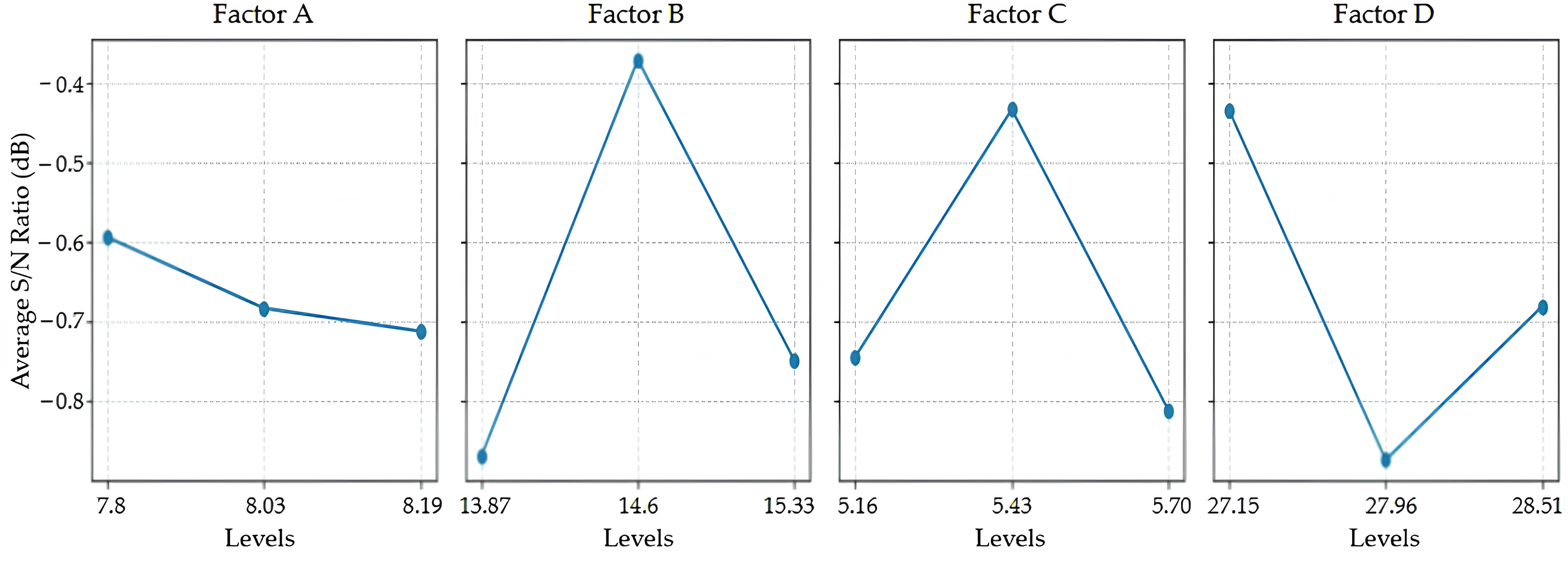
The main effects of the hyperparameters on the response value, expressed in terms of the average S/N ratio, are shown in
Figure 6. The larger the value of a factor’s main effect at a certain level, the greater its influence on the response compared to the other factors.
From
Table 10, it can be seen that factor B has the greatest impact on the
F1-Score, followed by D, C, and A. The optimal hyperparameter configuration, shown graphically in
Figure 6, was as follows: A = 7.8 M, B = 14.6 G, C = 5.43 s, and D = 27.15 ms. ANOVA was used to verify the statistical significance of the experimental results obtained from applying the Taguchi method. Assuming the hypotheses of independence and no interaction between the selected hyperparameters, One-Way ANOVA was adopted to determine the effect of varying individual factors on the
F1-score. The ANOVA results are shown in
Table 11.
The contribution of each hyperparameter to the
F1-score total variation was calculated as a percentage using the following Equation (31):
Equation (31) represents the proportion of the F1-score variability explained by a single hyperparameter. The higher that percentage, the greater the effect of that factor on response behaviour.
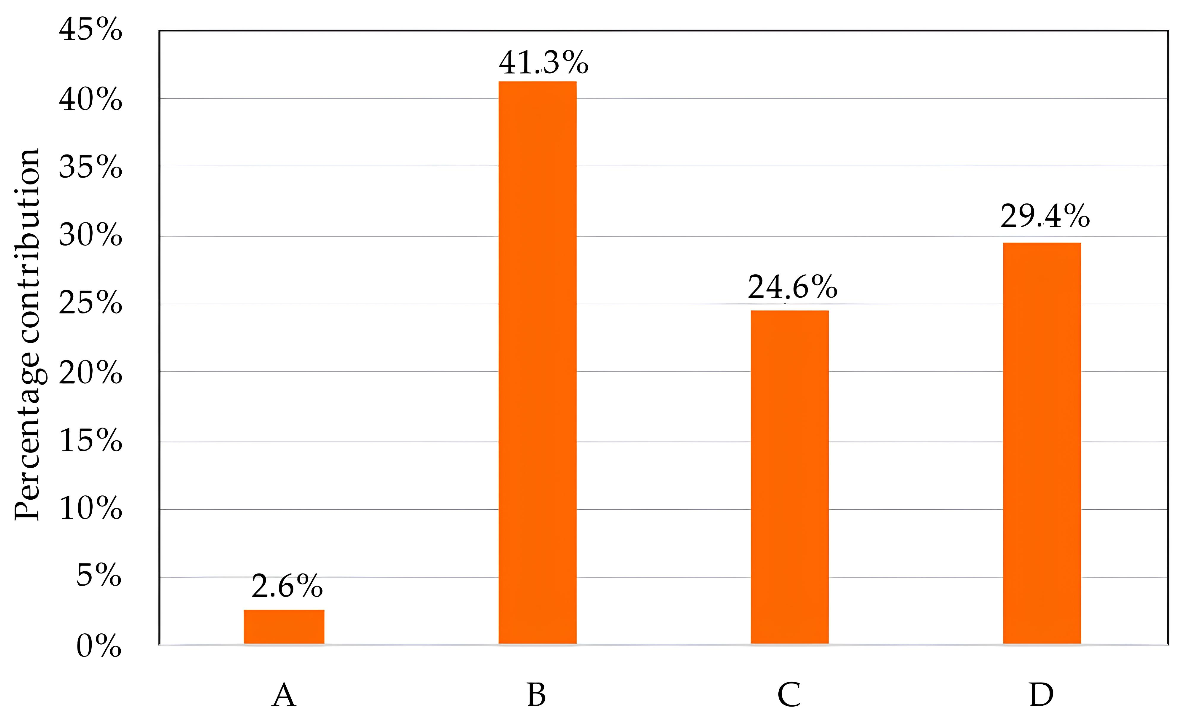
These percentage values are summarized in
Table 12 and graphically represented in
Figure 7.
From
Table 11 and
Table 12 and
Figure 7, FLOPs were found to be the statistically most influential hyperparameter on the
F1-score (41.3%), followed by Time per Image and Inference Time (29.4% and 24.6%, respectively), while Parameters had a negligible impact (2.6%).
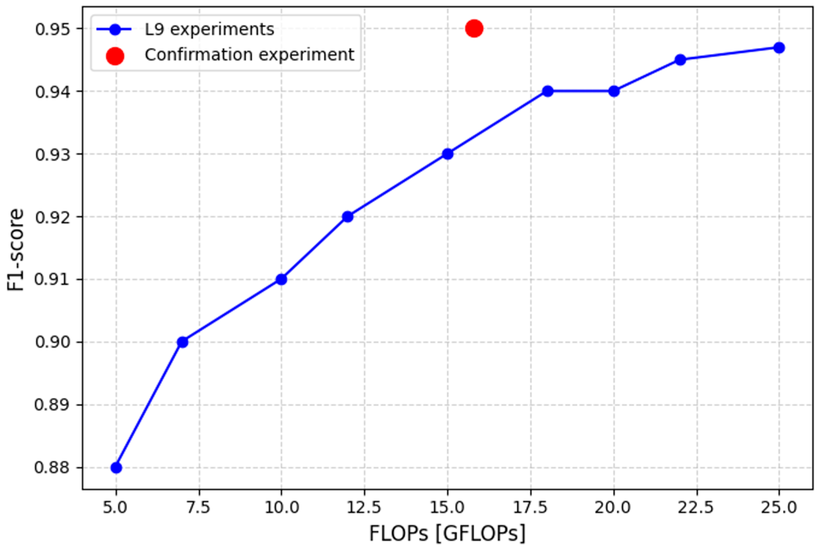
To further validate the predictive capability of the Taguchi–ANOVA framework, a confirmation experiment was conducted using a hyperparameter configuration outside the original L9 orthogonal array. The selected configuration explores a slightly broader computational regime while remaining compatible with real-time implementation constraints. The confirmatory experiment yielded an
F1 score of 0.95 (
Table 13), which is consistent with the trends predicted by the Taguchi analysis. In particular, the result confirms the dominant influence of FLOPs on segmentation performance, while showing a slight saturation of performance due to inference constraints. This result demonstrates that the Taguchi–ANOVA approach is not only descriptive but also predictive, providing reliable guidance for the selection of efficient and implementable model configurations.
The confirmation point is shown in
Figure 8, where the predicted trend confirms the robustness and predictive power of Taguchi–ANOVA optimisation.
The ANOVA validated the experimental results of the Taguchi method, statistically confirming the accurate performance of the U-Net model in identifying thermal anomalies in generic PCBs. The combination of U-Net segmentation, physically grounded feature extraction, and MLP classification offers an interpretable AI framework aligned with PCB thermal physics, which represents a key advantage for deployment in real engineering contexts. Current studies have looked at the use of anomaly detection in relation to applications that involve PCBs, using various datasets and learning models. For example, studies have been conducted that use adaptive temporal feature mapping combined with XGBoost classification algorithms that reached high accuracy in classifying process-related signals [
87,
88].
Others have looked at non-optical methods, like ultrasonic guided waves coupled with machine learning algorithms, for hot spots in printed circuit boards [
89,
90]. Although these approaches demonstrate good performance in their specific domains, they primarily focus on process-level data or alternative detection techniques. A qualitative comparison between these representative approaches and the proposed hybrid framework is summarised in
Table 14.
Conversely, the proposed model operates directly on high-resolution infrared thermograms, enabling spatiotemporal thermal analysis, real-time inference on embedded hardware, and statistically guided optimisation through the Taguchi–ANOVA methodology. These characteristics collectively distinguish the present study from existing approaches, particularly in terms of implementation-oriented real-time thermal monitoring and physically interpretable decision-making.
5. Conclusions
Ensuring reliable thermal behaviour in electronic systems is increasingly critical as device miniaturization and power density continue to rise. Monitoring the thermal stress of such devices is fundamental to contain thermal degradation, prevent failures, and avoid hazardous situations for both humans and the environment. For example, localized overheating within medical devices can cause damage to biological tissues or system failures, both with serious clinical consequences. To overcome the limitations of traditional thermal monitoring methods, which generally have low spatial resolution and are unsuitable for providing continuous real-time diagnostics, this paper proposes an integrated framework that IR, artificial intelligence, the Taguchi method, and ANOVA. The novelty of this approach lies in the use of Genichi Taguchi and Ronald Fisher’s methodologies to statistically confirm the performance of the proposed AI algorithms. In this study, passive thermography was applied to analyse the thermal behaviour of a generic PCB during its normal operation. IR images acquired using a FLIR P660 thermal camera, characterized by high spatial resolution, were used as input for training the AI model. The structure of this artificial intelligence pipeline, developed to improve real-time diagnostics in PCBs, first involves binary segmentation of IR images using the U-Net architecture, with the aim of discriminating the areas of the PCB most susceptible to thermal stress. The result is a binary mask in which each pixel of the original thermal image has been labelled as anomalous (1) or normal (0), depending on the temperature value detected. Subsequently, through thermal diffusion analysis, the propagation of heat in PCBs is described from a mathematical perspective. Specifically, a series of physical quantities known as descriptors were calculated and assembled into a feature vector. This vector was subsequently used as input for the heat diffusion model classification algorithm, the Multilayer Perceptron (MLP). It is capable of identifying four distinct categories of heat transfer: Localized Hotspot, Diffuse Anomaly, Asymmetric Propagation, and Uniform Heating. Although the implemented AI model significantly improved the quality of the acquired data through denoising, reconstruction, and super-resolution operations, the application of statistical methods ensures the scientific rigor of the results. Specifically, the use of Taguchi methodology and ANOVA allows us to go beyond simply observing a qualitative improvement. The optimal set of parameters allowed for achieving high F1-score values, demonstrating the high-performing predictions of the U-Net architecture. The optimised U-Net was compared to a standard baseline, showing a significant improvement in metrics and a reduction in inference times. While U-Net helps improve the starting data, the combined application of Taguchi and ANOVA allows for the validation and optimization of the entire workflow, ensuring that the results are not only more accurate but also reproducible and scientifically sound. It should also be noted that the system illustrated can be used in the thermal behaviour analysis of electronic devices employed in different application contexts. The integrated system facilitates predictive maintenance and real-time thermal quality control of electronic devices, improving their safety and efficiency under the various operating conditions they are subjected to. Despite its advantages, the integrated system presented still requires long processing times for results and the use of expensive equipment. Furthermore, it involves the device being taken out of service, as the object under examination is disassembled during the analysis and therefore cannot fulfil its intended purpose.
Future developments will therefore focus on creating miniaturized integrated systems that combine IR sensors and AI algorithms implemented on microprocessors. In addition, future studies will focus on adapting the pipeline to low-cost IR sensors and micro cameras that can be integrated into portable biomedical devices. These systems, installed directly inside biomedical devices or similar, will be able to perform thermal monitoring without affecting their functionality.




 ,
,