1. Introduction
Gallium-nitride (GaN) devices are emerging as a superior alternative to traditional silicon transistors in power-switching applications, primarily due to their exceptional ability to handle high currents and voltages [
1,
2]. The unique properties of GaN, such as wide bandgap, high electron mobility, and high thermal conductivity, make it an attractive material for next-generation power electronics. These features enable GaN devices to operate at higher efficiencies, frequencies, and temperatures than silicon-based counterparts, which is crucial for applications ranging from renewable energy systems to electric vehicles.
Despite their potential, GaN devices are currently facing challenges that impede their optimal performance. One of the most significant issues is the instability of the threshold voltage (V
TH) and the degradation of the dynamic on-resistance (R
ON) [
3,
4]. These limitations prevent GaN devices from achieving their anticipated performance levels, thus necessitating further research and development.
When GaN transistors are used in power switching converters, the most detrimental trap-related effect observed is the increase in dynamic R
ON beyond its static DC value. This leads to an undesirable rise in power losses [
5].
This dynamic R
ON can be attributed to various factors. For instance, carbon dopants introduced into the GaN buffer layer to enhance the blocking voltage [
6] may introduce undesired trap states. These traps become ionized under high drain voltages (V
DS) in the off-state [
7], leading to the exposure of negative charges that can partially deplete the two-dimensional electron gas (2-DEG), resulting in an increased R
ON when the device is switched back on.
However, buffer traps are not the only culprits contributing to dynamic R
ON. Surface states can similarly affect the on-state resistance. In fact, both buffer [
8] and surface traps [
9] are susceptible to ionization by high off-state drain voltages and hot-carrier effects. These issues are particularly pronounced under hard-switching (HS) conditions [
10], where the simultaneous presence of high voltage and current during transitions exacerbates degradation due to self-heating and hot electrons [
11].
The cumulative impact of these effects, along with off-state degradation mechanisms, leads to a significant drift in the device’s parameters. This highlights the importance of investigating the physical mechanisms responsible for device degradation, especially in HS operational modes. In this scenario, differentiating between hot-electron effects and off-state trapping/de-trapping mechanisms is rather challenging. Custom pulsed I–V (PIV) measurement setups are often used for this purpose [
10,
11,
12] and several approaches have been proposed in the literature with this aim. For instance, a resistive load with a parallel capacitance connected to the device under test (DUT) was utilized to mimic the HS trajectory in [
12], while a current limiting circuit was used in [
10] to control the off/on transitions at high drain voltages. An alternative approach involves commercial pulsed IV systems, but these can be prohibitively expensive and not readily available in smaller research centers.
In this work, we propose an alternative method to investigate hot electron effects using a commercially available parameter analyzer. The concept is rather simple: hot electron effects can be examined through fast on-state stress tests at high voltages [
13], thereby avoiding self-heating effects and dynamic R
ON increases due to off-state stress that are typically observed after relatively long stress times [
14,
15].
This hot electron trapping mechanism could occur within the GaN buffer or at the device’s surface [
13], highlighting the need to distinguish these contributions to accurately understand the underlying physics. In this framework, the proposed method serves as a powerful tool since, by monitoring parameter recovery after stress, it can provide more insights on trap dynamics. Additionally, preliminary characterization under static off-state stress [
16] is used to determine the extent of degradation without hot-electron involvement, providing a baseline for comparison and validation of the proposed methodology.
In conclusion, advancing GaN technology is pivotal for the evolution of power electronics. By addressing the challenges of threshold voltage instability and dynamic RON degradation, we can unlock the full potential of GaN devices. The methods and approaches discussed here are instrumental in pushing the boundaries of GaN device performance, paving the way for more efficient and reliable power-switching applications that will benefit a wide array of industries.
The paper is organized as follows.
Section 2 reports a description of DUTs, while
Section 3 shows a preliminary characterization used to put in evidence the role of buffer traps. Then,
Section 4 shows the results obtained under PIV characterization. The proposed approach is described in
Section 5, while in
Section 6 we present the experimental results obtained. Finally, conclusions are drawn in
Section 7.
3. Preliminary Characterization
In order to have some preliminary information on the degradation mechanisms that could affect the DUTs, we carried out static off-state stress tests according to the sequence shown in
Figure 2.
The stress/measurement sequence is rather simple. First, the fresh current level (I
D0) is acquired at V
DS = 0.5 V, V
GS = 6 V to set a reference value for this parameter. Then, a static off-state stress is applied to the DUT for 1000 s with V
DS,off = 25 V and V
GS,off = 0 V. This stress time was sufficient to induce a steady-state degradation of the tested samples, since a further increase in the stress time beyond 1000 s was not producing any further current collapse. After the stress phase, a 1000 s measurement time was employed to monitor the on-state current recovery after the stress removal. In this phase, V
DS,recovery was set to 0.5 V, while V
GS,recovery was fixed to 6 V to bias the DUT in its linear region. This V
GS,recovery value (i.e., 6 V) was chosen in order to bias the DUT in a typical application condition, since tested devices are commonly turned on at V
GS = 6 V to correctly operate in their linear region. A logarithmic sampling rate was used to acquire the current evolution over several time decades [
18]. To this end, the rapid block mode acquisition of the digital sampling oscilloscope (DSO) was used, exploiting the segmented memory of the instrument. Particularly, during the recovery monitoring, the first point was acquired about 25 ms after the stress removal.
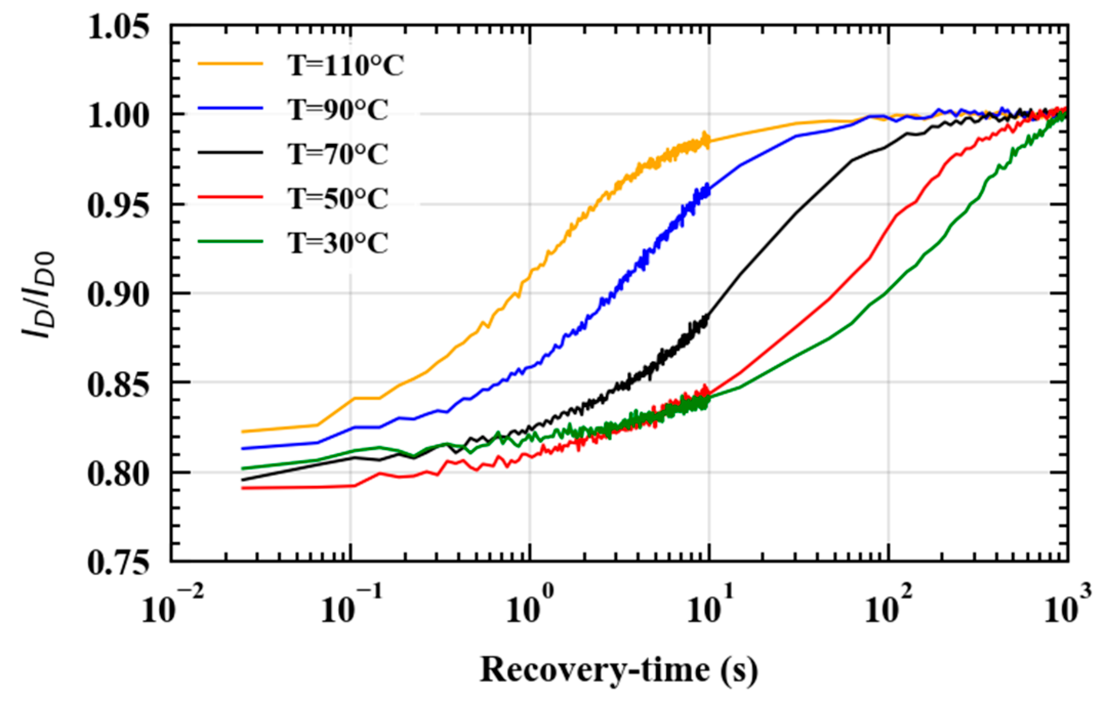
The measurements were performed at different base plate temperatures in order to evaluate the temperature effect on the dynamics of the current recovery transients (see
Figure 3). Accordingly, the choice of such a low voltage (V
DS,off = 25 V) was important to reduce the electric field impact on the traps capture/emission process, thus limiting any E-field impact on the time constant extraction.
This technique is typically employed to investigate the physics governing trap states in semiconductor devices and is functional to understand the nature of traps ionized by static off-state stress. The information acquired at this step will be important to debug the method proposed in
Section 5.
As we can see by looking at
Figure 3, the degradation induced by the static off-state stress was completely recoverable and the recovery transients took about 1000 s to reach its steady state at 30 °C. Moreover, the current recovery transients sped up while increasing the base-plate temperature, consistent with a thermally activated charge emission process [
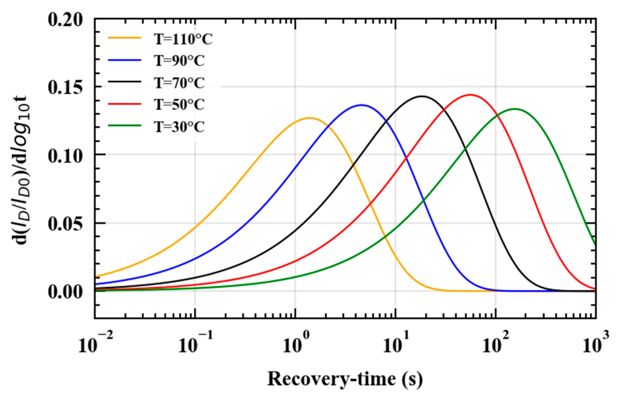
19]. In order to gain physics insights on the trap states involved, we fitted the current transients by means of stretched exponential functions [
20,
21] and we extracted the transients time constant in correspondence to the peak of the derivative signals reported in
Figure 4. Moreover, the derivative peak provided an indication on the transient amplitude, showing good consistency with the data reported in
Figure 3.
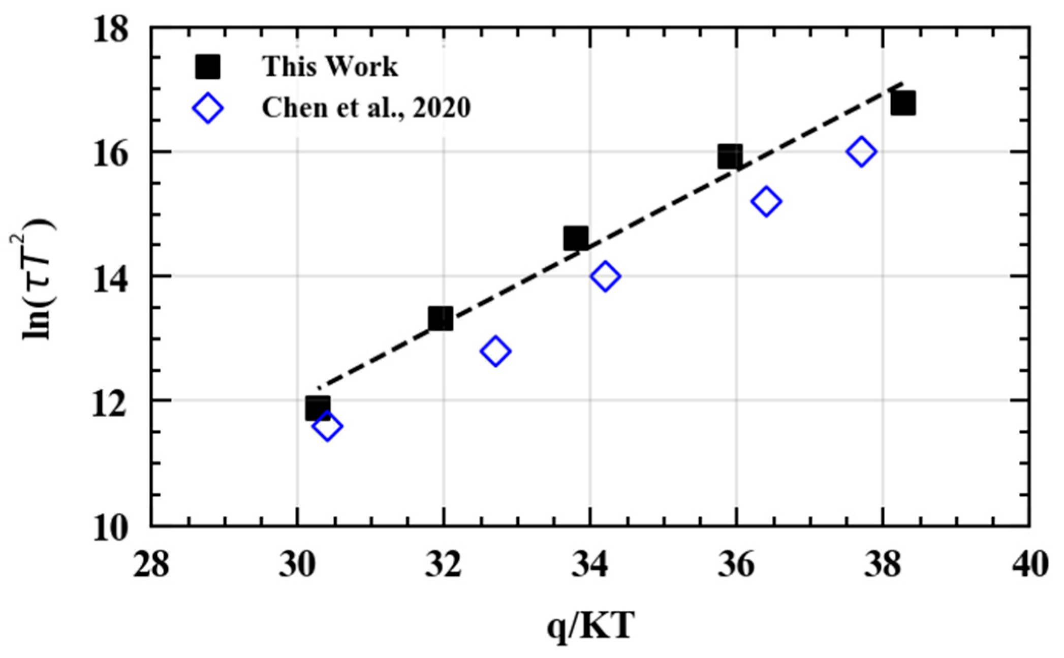
The emission time constant extracted was then used to reconstruct the Arrhenius plot shown in
Figure 5, according to the logarithmic form of the Arrhenius equation [
22]. To verify the involvement of buffer traps, the Arrhenius plot obtained in this work was compared to the one reported in a previous paper in which the trapping/de-trapping mechanism was associated with the ionization of carbon-related acceptors in the buffer layer [
23].
The fact that similar slopes and coordinates were obtained in the Arrhenius plots of
Figure 5 suggests that the trapping mechanism responsible for R
ON degradation was likely to be the same. Moreover, we extracted activation energy (E
A) and the trap’s cross section (σ) from the slope of the linear fit of the points in the Arrhenius plot and from the intercept with the y-axis, respectively. The values extracted were E
A = 0.61 eV and σ = 1.7 × 10
−18 cm
2. These values are totally consistent with those extracted from the points in [
23] (i.e., E
A= 0.63 eV and σ = 3 × 10
−18 cm
2). It is true that capture cross sections in the range between 1 × 10
−16 cm
2 and 5 × 10
−19 cm
2 have also been reported for interface states in [
24]. However, it is the combination of E
A and σ that defines the traps states involved and the cross section by itself is not sufficient to fully describe the trapping mechanism. Concerning this point, a similar combination of E
A and σ was reported in [
25] in which E
A = 0.61 eV and σ = 5.5 × 10
−18 cm
2 have been extracted. In [
25], this combination of E
A and σ was demonstrated to be related to the emission of holes from carbon-related acceptors in the GaN buffer. Accordingly, the current collapse induced by the applied off-state stress in this work could be associated with the ionization of carbon acceptors in the buffer layer [
25,
26,
27], as suggested by previous literature [
23], and the current recovery observed in the following 1000 s can be ascribed to the redistribution of charges in the GaN buffer, restoring the 2-DEG conductivity [
28]. Identical results have been observed on Type B samples (not shown), indicating that the degradation mechanism occurring under off-state stress conditions is the same among the two devices. This is totally consistent with the fact that the current collapse induced with static stress is due to carbon traps in the buffer, since the buffer design is the same for Type A and Type B samples. This result already provides an interesting picture of the physical mechanism affecting the device behavior under static off-state stress. Nevertheless, we wanted to test the device’s behavior under switch-mode conditions, for two important reasons: (i) this condition is closer to the final operative scenario of the DUTs; and (ii) in this way we could evaluate hot-carrier effects, since hot electrons could come into play during transitions led at non-zero current. For this reason, pulsed I–V characterization under both soft-switching and hard-switching conditions was needed to correctly benchmark the technique proposed in
Section 5 for hot-electron characterization.
4. Pulsed I–V Characterization
To have a mean of comparison for the proposed technique, pulsed I–V characterization was first performed on the DUTs. To this end, a stress/measurement sequence was implemented with the AM200 PIV system by AMCAD (see
Figure 6). The AM200 system was then connected to the probe station to perform the pulsed I–V characterization on 8-inch wafers.
Before starting the stress phase (1), the fresh ID-VGS characteristic was reconstructed by means of a sequence of gate pulses (2 μs) ranging from 0 V and 6 V, while the device’s VDS was at VDS,on = 0.5 V. Then, a 1000 s stress was performed at VDS = VDS,off, VGS,off = 0 V. During the stress, the device was periodically turned on with a 100 µs switching period and 2% duty cycle to mimic conventional switch mode operation. After the stress (2), the gate voltage was pulsed again to capture the stressed ID-VGS characteristics. At the same time, the drain voltage was briefly pulsed to VDS = VDS,on with short (2 µs) on-state time intervals separated by 100 µs off-state biasing. During this off-state time, the stress voltage (VDS,off) was still applied to the DUT, to reduce the parameters recovery.
The stress/measurement sequence just described was then used to characterize Type A and Type B devices under both soft- (SS) and hard-switching (HS) mode (see
Figure 7).
Particularly, SS conditions were first considered, in which the high/low and low/high VDS transitions were performed at zero current. This condition is meaningful for some key applications (e.g., LLC resonant converters) in which the transistors used as switches experience this kind of switching trajectory.
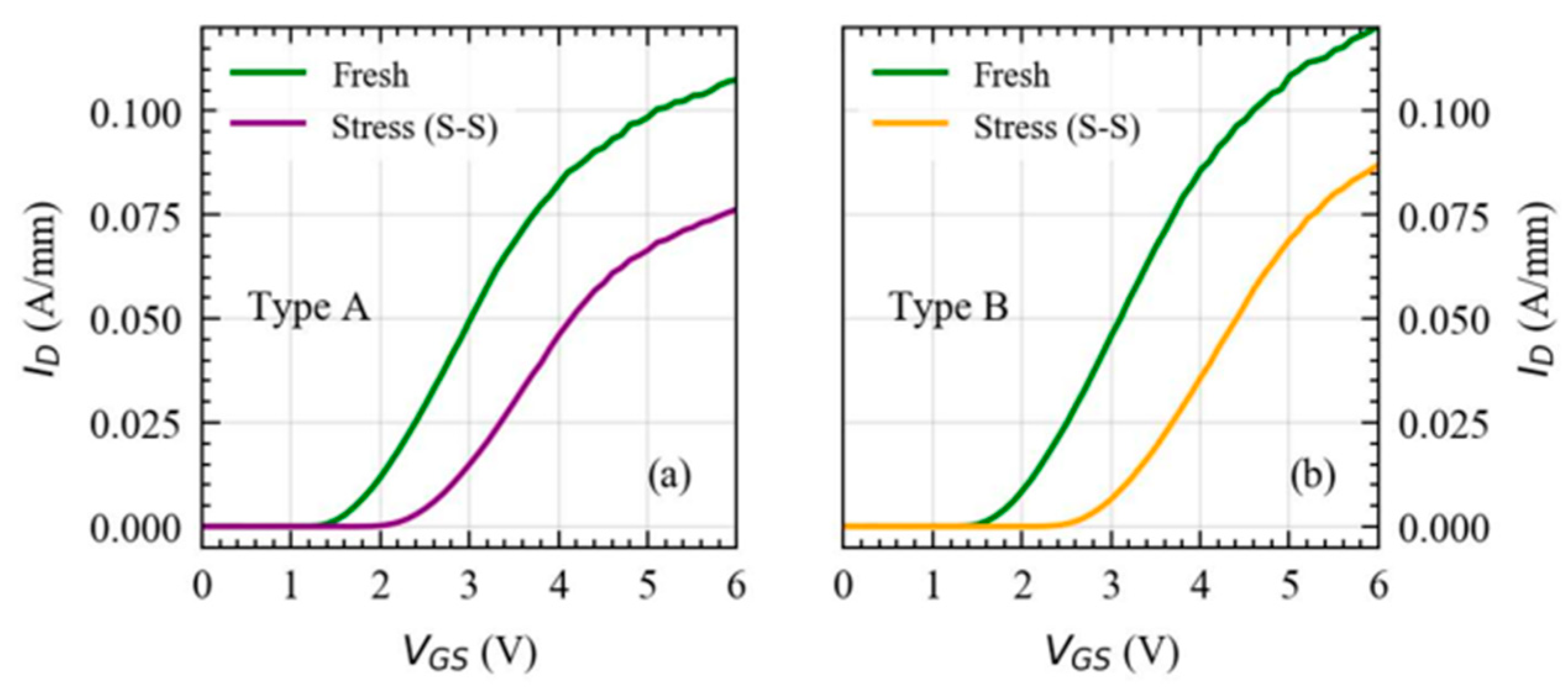
The results obtained under SS mode are shown in
Figure 8.
Similar results were obtained for Type A and Type B devices under SS mode operation. This suggests that the different surface treatments employed do not significantly affect the dynamic-R
ON under off-state stress conditions if SS mode is considered. In fact, in this operative mode, buffer traps are expected to be dominant, as already highlighted by the preliminary characterization in
Section 3. On the other hand, the role of surface traps may be more evident under HS mode, in which hot electrons may come into play.
Accordingly, we performed the same characterization under HS mode conditions, for which the results obtained are reported in
Figure 9.
Looking at
Figure 9, we can clearly see that the results obtained under HS conditions present a larger degradation in both V
TH and R
ON parameters (see
Figure 8 for comparison). This means that transitions performed at relatively high voltage and current levels introduce additional drifts that could be due to hot carriers’ effects. Particularly, a different behavior was observed for Type A and Type B devices. In fact, the Type A device presented a fully collapsed current after 1000 s stress, stemming from a larger degradation with respect to the Type B device. The fact that different behaviors were observed for Type A and Type B devices suggests the involvement of hot electrons trapping at the device’s surface, since the surface treatment was the only difference between the two device types. Our purpose was next to verify whether the same trends and conclusions could be obtained by means of the method introduced in the next section.
5. Alternative Method
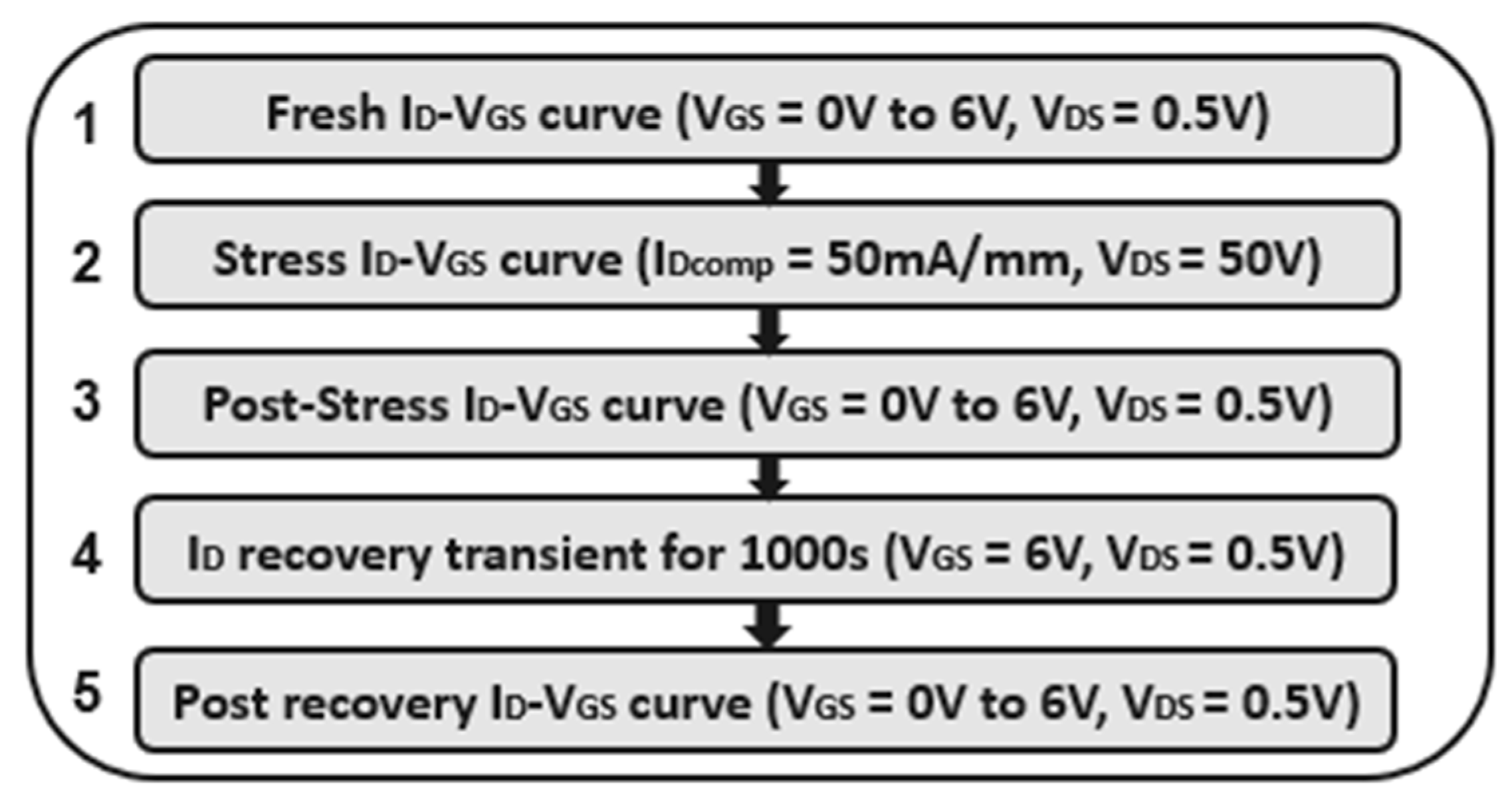
The measurement sequence implemented with the B1505a parameter analyzer is schematically depicted in
Figure 10.
- (i)
A fresh ID-VGS curve of the DUT was measured to set a reference value for the device’s parameters. To this end, VDS was kept at 0.5 V, while VGS was swept from 0 V to 6 V to extract VTH and RON;
- (ii)
The on-state stress test was performed by reconstructing a fast (~ms) ID-VGS curve at VDS = 50 V. Particularly, the VGS was rapidly increased from 0 V till a limit VGS for which the chosen current compliance (e.g., 50 mA/mm) was reached. It is important to stress the fact that the time required to sweep the VGS should be short enough to avoid second order effects and/or device failure. This is mainly related to the fact that a long on-state stress could bring the DUT out from its safe operating area (SOA) due to self-heating effects;
- (iii)
The post stress ID-VGS was acquired at VDS = 0.5 V, while VGS was swept from 0 V to 6 V;
- (iv)
ID was monitored for 1000 s with VDS = 0.5 V and VGS = 6 V to measure the current recovery with logarithmically spaced samples. This allowed us to evaluate the current dynamics over several time decades;
- (v)
The I
D-V
GS curve after 1000 s recovery was acquired at V
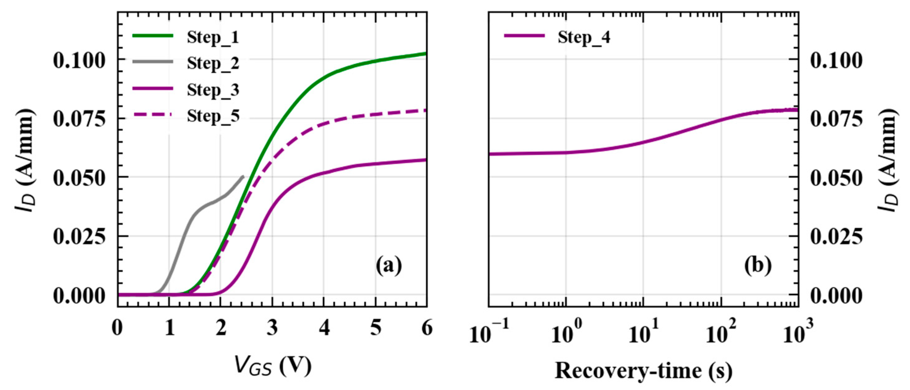
DS = 0.5 V to measure the retained degradation. An example is shown in
Figure 11.
Figure 10.
Measurement sequence applied for the evaluation of power devices’ degradation under on-state stress conditions.
Figure 10.
Measurement sequence applied for the evaluation of power devices’ degradation under on-state stress conditions.
Figure 11.
Example of curves acquired during the different steps of the measurement procedure. (a) ID-VGS curves captured during Steps 1–2–3 and Step 5; (b) current recovery transient measured during Step 4.
Figure 11.
Example of curves acquired during the different steps of the measurement procedure. (a) ID-VGS curves captured during Steps 1–2–3 and Step 5; (b) current recovery transient measured during Step 4.
The I
D-V
GS measured at V
DS = 50 V during Step 2 allowed us to emulate on-state stress conditions and induce the trapping of hot electrons. The curve reconstructed during this step present reduced V
TH with respect to the fresh one. This effect could be explained by the drain-induced barrier lowering (DIBL) effect [
29] that appears when short channel devices are biased at large drain voltages. When the current compliance is reached, the on-state stress is removed and the post-stress I
D-V
GS is measured, showing a positively shifted V
TH and a reduced triode current. This indicates the presence of hot-electron trapping under the gate terminal and in the gate-drain access region. The I
D-recovery transients monitored in the following 1000 s allowed us to capture the dynamics of traps in the buffer layer, which should present time constants in the order of several tens of seconds at 30 °C [
14] (see
Section 3). After this recovery time, the I
D-V
GS measured during Step 5 showed a completely recovered V
TH, indicating that trapped electrons below the gate terminal presented time constants shorter than 1000 s. Conversely, the trapping that occurred in the gate-drain access region could be only partially recovered after 1000 s, suggesting the presence of two different mechanisms affecting the R
ON-degradation, whose contributions can be discerned by the proposed measurement.
6. Experimental Results and Discussion
At this point, the proposed approach was applied on both type A and Type B samples, with the aim to compare DUTs featuring the same buffer design, but different surface treatment. The results obtained on Type A and Type B devices at 30 °C are shown in
Figure 12.
The device featuring Type A treatment showed an evident current collapse after the application of the on-state stress (see Step 3 in
Figure 12a). On the other hand, the I
D-V
GS curve acquired after stress for treatment B showed reduced parameter degradation, consistent with the behavior captured by PIV measurements. This evidence suggests that part of the degradation could be associated with surface traps. This is further confirmed by a reduced degradation retained after 1000 s recovery for Type B devices, stemming for the presence of an optimized surface (see
Figure 12b). As highlighted previously, this retained degradation affects only the device’s R
ON, whereas the device’s V
TH is completely recovered. This indicates that the retained current reduction after 1000 s is due to the trapping effect that takes place in the access regions. Another important aspect refers to the I
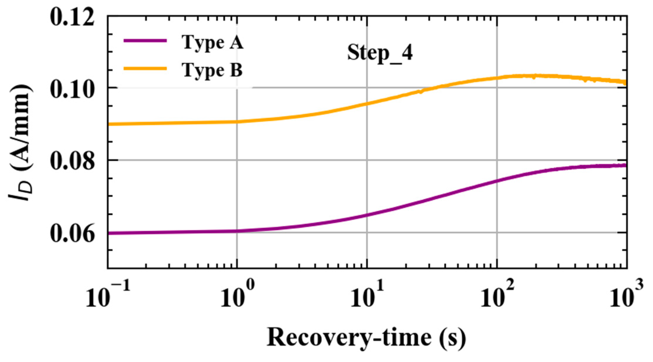
D recovery transient monitored during Step 4. In fact, the I
D recovery transients obtained for the two different surface treatments showed similar time constants and amplitudes (see
Figure 13).
This suggests that the physical mechanism governing the recoverable degradation was the same for both devices. Moreover, the transient time constant was compatible with the one expected for buffer traps in GaN [
15] (see
Figure 3 for comparison). Particularly, the current reduction associated with this process could be due to the ionization of carbon acceptors that partially deplete the 2-DEG [
30]. This observation is consistent with the C-doped buffer featured by the DUTs and the preliminary characterization presented in
Section 3. According to this hypothesis, the recovery transient observed should be due to the redistribution of charges in the GaN buffer after the stress removal [
28], which restores the 2-DEG conductivity. The fact that similar I
D transient amplitudes were obtained on Type A and Type B devices is in line with the fact that the DUTs shared the same buffer design.
The different configurations that the DUTs showed during the characterization steps can be better explained thanks to the band diagram sketched in
Figure 14.
During Step 1, the fresh I
D-V
GS characteristic is acquired and the 2DEG is formed at the AlGaN/GaN interface. C-related acceptor traps are at equilibrium and are neutral (see
Figure 14a). During Step 2, the applied on-state stress yields the trapping of hot electrons at the device’s surface (i.e., at the AlGaN/SiN interface). At the same time, hot carriers favor the ionization of C-related acceptors that become negatively charged by emitting holes in the valence band. The increased negative charge at both surface and buffer layer causes the partial depletion of the 2DEG due to an upward shift of the bands (see
Figure 14b). During 1000 s recovery time (Step 4), holes redistribute in the buffer and are trapped back in their previously ionized acceptor states. Accordingly, during Step 5, C-related acceptors in the buffer are neutralized and partially repopulate the 2DEG. The retained hot electrons at the surface, conversely, are still present during Step 5 and yield a not completely recovered 2DEG density (see
Figure 14c). This causes a not completely recovered R
ON.
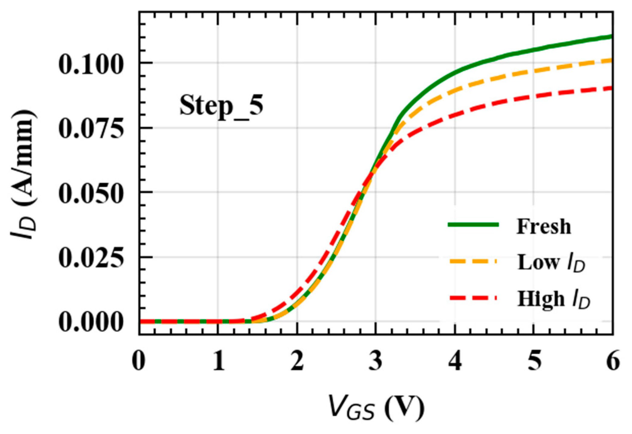
Another important aspect refers to the concentration of free charges that can contribute to the on-state degradation. In fact, the current level at which the on-state stress is performed could affect the probability of generating hot electrons responsible for current collapse. According to this observation, we performed the same characterization on Type B devices for two different compliance levels, shown in
Figure 15.
It is important to mention that the low I
D and high I
D tests in
Figure 15 were performed on the same device, in this order, separated by one week of time. This elapsed time between the two tests was sufficient for a complete R
ON recovery to its fresh value. Conversely, a slight decrease in the V
TH was observed. This slight difference in V
TH is still under investigation. However, V
TH was still in a reasonable range and did not impact the following analysis, which is more focused on the R
ON behavior.
The curves reported in
Figure 15b show that an increase in the current compliance yields an increased degradation induced by the on-state stress. This is consistent with the increased free carrier’s concentration. This confirms once again the involvement of hot electrons and can further help in the understanding of underlying physics [
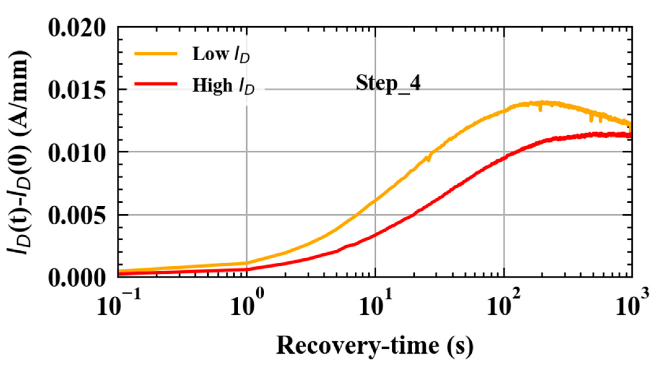
31]. To this end, a relevant indication is provided by the transients shown in
Figure 16.
As we can see, the current transients obtained during Step 4 still presented similar time constants and amplitudes, indicating that an increase in the current density does not affect this process.
This is consistent with the interaction of hot electrons with buffer traps, since the trapping/de-trapping in the buffer layer does not require large current levels to be triggered. Conversely, the increased degradation observed in
Figure 15b at higher compliance could be associated with the capture of hot electrons at the device surface. In fact, the hot carriers should overcome a large potential barrier to be captured in the device’s surface [
12] and this makes this process more difficult. Accordingly, an increase in the current level during the high voltage stress increases the probability of the hot electrons being trapped in this region. This is confirmed by the I
D-V
GS curves shown in
Figure 17.
The retained degradation captured after 1000 s from the stress removal increases while increasing the current compliance. As previously observed, the contributions related to buffer traps are already recovered after this relaxation time, suggesting that the remaining contribution should be related to a different location. Particularly, the retained trapped charge is located in the gate-drain access region (mainly affecting RON), consistent with trapping at the surface. Moreover, this retained degradation was proven to be dependent on the surface treatment, further confirming the involvement of surface traps.
