Abstract
In this work, we synthesized a lead-free halide double perovskite, Cs2CuSbCl6, with high carrier mobility via a one-pot hot-injection method. When combined with a high-resistivity silicon wafer, it forms a Type-II heterojunction structure, and its modulation depth reaches 84% by adjusting the annealing temperature. It demonstrates promising modulation performance at 532 nm. Owing to its strong absorption in the ultraviolet region, Cs2CuSbCl6 shows potential for application in ultraviolet-controlled terahertz modulation.
1. Introduction
Owing to their wide bandwidth and high data transmission rate [1], terahertz waves have emerged as a major research focus in the future 6G communication field. The regulation of terahertz waves is therefore a key issue in the field of terahertz communications [2,3]. In this work, we focus on silicon-based terahertz modulators. Benefiting from silicon’s low cost and high compatibility with CMOS technology, such modulators are more conducive to large-scale applications in future communication scenarios. Terahertz modulators are categorized into optical modulators and electrical modulators. Optically controlled modulators exhibit lower insertion loss and, furthermore, are not limited by the resistance–capacitance (RC) time constant of devices [4], thus offering more advantages over electrically controlled modulators. In recent years, heterojunction engineering has been widely applied in various fields of device fabrication [5,6]. Due to the low modulation efficiency of silicon, we combine perovskite with silicon to form a heterojunction, aiming to enhance its electrical conductivity and carrier mobility for improved modulation performance. Perovskite materials have been extensively studied in the photovoltaic field due to their high carrier mobility [7,8,9], and in recent years, they have also been gradually applied to the terahertz field [9,10].
Lead-free halide perovskites have gradually replaced traditional lead-based halide perovskites due to their advantages, such as being environmentally friendly, non-toxic, and having a high light absorption coefficient [11,12,13]. In 2020, Zhou et al. developed a novel lead-free halide perovskite—Cs2CuSbCl6—and demonstrated that it serves as an excellent light-absorbing layer for perovskite solar cells [14]. In 2024, Hicham El-Assib et al. obtained a theoretical efficiency of 27% for Cs2CuSbCl6-based lead-free double perovskite solar cells via theoretical calculations [15]. In 2022, Yashaswi Soni et al. confirmed through theoretical calculations that Cs2CuSbX6 (X = Cl, Br, I) possesses a high dielectric constant, low electronic effective mass, and high carrier mobility [16]. However, experimental studies on terahertz devices based on Cs2CuSbCl6 have not been reported yet.
This paper applies Cs2CuSbCl6 to the field of terahertz modulation. This work synthesized Cs2CuSbCl6 via a one-pot hot-injection method and measured the terahertz time-domain spectroscopy (THz-TDS) of the Cs2CuSbCl6/Si heterojunction structure in the range of 0.4–1.6 THz under 532 nm laser excitation. The maximum modulation depth experimentally measured reaches 84%.
2. Material Synthesis and Characterization
2.1. Synthesis and Characterization of Cs2CuSbCl6 Sample
Materials: Copper(II) acetate (Cu(OAc)2, purity ≥ 98%, Aladdin, Shanghai, China), antimony(III) acetate (Sb(OAc)3, purity 97%, Aladdin), cesium acetate (Cs(OAc), purity ≥ 95%, Aladdin), trimethylchlorosilane (TMCS, purity 98%, Aladdin), 1-octadecene (purity ≥ 90%, Aladdin), oleic acid (reagent grade, Macklin, Shanghai, China), oleylamine (purity > 90%, Adamas, Shanghai, China), toluene (analytical grade, Tianjin Fuyu Fine Chemical Reagent Co., Ltd., Tianjin, China), n-hexane (analytical grade, Tianjin Fuyu Fine Chemical Reagent Co., Ltd.). All reagents were used without further purification.
Synthesis of Cs2CuSbCl6 nanocrystals via a one-pot hot-injection method: 0.65 mmol of cesium acetate, 0.22 mmol of copper acetate, and 0.5 mmol of antimony acetate were added to a two-necked flask. Subsequently, 10 mL of 1-octadecene, 2.9 mL of oleic acid, and 0.65 mL of oleylamine were introduced into the flask. First, vacuum evacuation was performed at 105 °C for 1 h, followed by heating to 165 °C under a nitrogen atmosphere. At 165 °C, 0.4 mL of trimethylchlorosilane (TMCS) was injected. When the temperature reached 170 °C, the reaction mixture was rapidly quenched in an ice-water bath for 1 min. The resulting solution was centrifuged at 9000 rpm for 10 min, and the supernatant was discarded. The precipitate was washed with 10 mL of toluene three times. Subsequently, the cleaned precipitate was dissolved in 5 mL of n-hexane and sonicated for 10 min. The solution was then centrifuged at 5000 rpm for 10 min, and the supernatant was collected as the Cs2CuSbCl6 nanocrystals.
Material Characterization: The nanocrystal precipitate washed with toluene was used for structural characterization via powder X-ray diffraction (XRD) measurements. The results are basically consistent with the XRD pattern reported in the literature [17], as shown in Figure 1. In addition, both the absorption spectrum and band gap diagram of the as-synthesized Cs2CuSbCl6 nanocrystals are consistent with the literature reports [17], further verifying the success of the nanocrystal synthesis. The (210) crystal plane was selected for analysis, and the Scherrer equation was employed for calculation. For the (210) plane, the full width at half maximum (FWHM) is 0.3°, the diffraction angle 2θ is 19.7°, and the X-ray wavelength is 0.15406 nm. The calculated grain size is 27 nm, which is consistent with the value reported in Ref. [17]. In addition, scanning electron microscopy (SEM) experiments were performed on all samples, as detailed in Supplementary Material Figure S1.
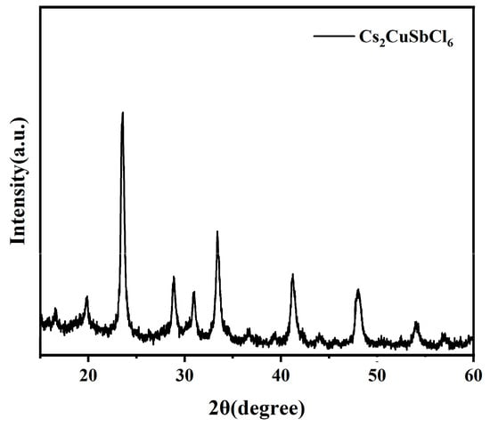
Figure 1.
XRD pattern.
2.2. Preparation of Thin Films
A 10 mm × 10 mm × 500 µm high-resistivity silicon wafer was first ultrasonically cleaned in acetone, absolute ethanol, and deionized water for 30 min each, followed by an ozone treatment in an ozone cleaner for 15 min. The as-prepared Cs2CuSbCl6 nanocrystal solution was sonicated for 5 min to achieve a uniform dispersion of the crystals. Using a pipette, the Cs2CuSbCl6 solution was dropped onto the surface of a bare silicon substrate and spin-coated at a rotation speed of 2000 rpm for 30 s, completing one spin-coating cycle. The thickness of the film was adjusted by increasing the number of spin-coating cycles. After spin-coating, the silicon substrate was placed on an annealing stage for annealing for 30 min. In this experiment, Sample 1 (thin film) was fabricated via three spin-coating cycles followed by annealing at 100 °C. While maintaining the same number of spin-coating cycles, Sample 2 was obtained by annealing at 120 °C; Sample 3 was prepared by annealing at 150 °C with the same spin-coating cycles; Sample 4 was fabricated via annealing at 180 °C under identical spin-coating conditions; and Sample 5 was obtained by annealing at 210 °C while keeping the number of spin-coating cycles unchanged.
The ozone treatment process was conducted using an ozone cleaner (Model: PSD Pro Series, Novascan Technologies Inc., Boone, KY, USA, operating on the principle of UV–light excitation of oxygen to generate ozone) under room temperature and atmospheric pressure. While ultrasonic cleaning can remove most visible impurities, trace organic residues, weakly adsorbed inorganic particles, and metallic contaminants may still remain on the silicon substrate surface. Ozone exhibits strong oxidizing properties and decomposes into reactive oxygen atoms during treatment, which oxidize residual organic matter into CO2 and H2O, while also inducing oxidative modification of inorganic impurities, making them more easily detached from the substrate surface and thereby achieving atomic-level cleanliness of the substrate. Furthermore, after ultrasonic cleaning, the silicon substrate surface remains primarily covered with hydrophobic Si–H groups. Following ozone treatment, these Si–H groups are oxidized into hydrophilic Si–OH groups, which promote better spreading of the solution during spin-coating and improve the quality of the thin film.
2.3. Characterization Technology
The crystal structure of Cs2CuSbCl6 was characterized via X-ray diffraction (XRD, Model SmartLab SE, Rigaku Corporation, Tokyo, Japan). The UV-Vis diffuse reflectance spectrum of the Cs2CuSbCl6 sample was measured using a UV-Vis spectrophotometer (Model UV-2600i, Shimadzu Corporation, Kyoto, Japan). Furthermore, the secondary electron cutoff and valence band edge of the Cs2CuSbCl6 material were investigated via ultraviolet photoelectron spectroscopy (UPS, Model ESCALAB 250 XI, Thermo Fisher Scientific Inc., Waltham MA, USA). The surface and cross-sectional morphology of the Cs2CuSbCl6/Si composite were examined using scanning electron microscopy (SEM, Model Regulus 8100, Hitachi High-Technologies Corporation, Tokyo, Japan).
3. Terahertz Experiment
The terahertz time-domain spectroscopy (THz-TDS) of the samples was measured using a home-built THz-TDS system in our laboratory, which is coupled with a continuous-wave (CW) laser system to enable visible light excitation of the samples. The THz-TDS adopts a photoconductive scheme for terahertz generation and detection, utilizing a femtosecond laser with a central wavelength of 800 nm, a pulse duration of 100 fs, and a repetition rate of 84 MHz. The laser beam is split into two beams by a 50:50 beam splitter—one for terahertz generation and the other for terahertz detection. A CW semiconductor laser diode with a wavelength of 532 nm was used as the optical pump source, with a laser spot area of 4.1 cm2 and a terahertz spot area of 2.4 cm2. With air as the reference for the background signal, the terahertz time-domain spectra of the samples were measured under different laser power density conditions, and a Fourier transform was applied to extract corresponding information such as frequency and amplitude. The schematic diagram of the experimental setup is shown in Figure 2.
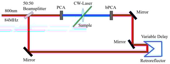
Figure 2.
Schematic diagram of THz TDS equipment.
The measured terahertz transmission results are shown in Figure 3a–f. As the pump laser power density increases continuously, the amplitude of terahertz waves decreases progressively, which indicates that all samples exhibit significant modulation effects on terahertz waves. Among them, Sample 4 demonstrates a superior modulation effect at each pump power. As presented in Figure 3f, the modulation effect of bare silicon is extremely weak—even at a laser power density of 2.2 W/cm2, its modulation effect on terahertz waves remains insignificant.
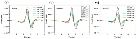
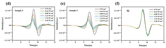
Figure 3.
Terahertz time-domain spectra (THz-TDS) of (a) Sample 1, (b) Sample 2, (c) Sample 3, (d) Sample 4, (e) Sample 5, and (f) bare Si under 532 nm laser excitation.
The transmittance T(ω) is calculated using the formula T(ω) = Es(ω)/Er(ω), where T(ω) denotes the transmittance of the sample, Es(ω) represents the Fourier-transformed frequency-domain signal of the sample, and Er(ω) is the Fourier-transformed frequency-domain signal of air (reference). As shown in Figure 4, at a pump laser power density of 0, the terahertz transmittance of all samples is nearly identical. With the continuous increase in pump laser power density, the terahertz transmittance of the samples decreases correspondingly. The Fabry–Pérot effect, caused by multiple reflections of terahertz waves inside the sample and at the sample–air interface, leads to obvious fluctuations in the terahertz transmission spectrum. Irradiation of the silicon substrate and Cs2CuSbCl6 by the pump laser generates photogenerated carriers, which alter the dielectric constant and electrical conductivity of the material, thereby resulting in a decrease in terahertz transmittance.
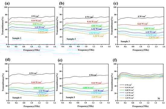
Figure 4.
Terahertz transmission spectra of (a) Sample 1, (b) Sample 2, (c) Sample 3, (d) Sample 4, (e) Sample 5, and (f) bare Si under 532 nm laser excitation.
To more intuitively demonstrate the terahertz wave modulation effect, the modulation depth (MD) of the samples was defined and calculated. The modulation depth is derived from the formula , where Tdark denotes the transmittance of the sample without laser irradiation, and Tlaser represents the transmittance with laser irradiation. Figure 5 presents the broadband terahertz modulation of all samples and the silicon substrate. Under pump light irradiation with the same power density, all samples exhibit a higher modulation depth than the silicon substrate at the same frequency. Figure 6 shows the variation in the modulation depth of the samples at 1.3 THz with the pump light power density. As the pump light power density increases, the modulation depth continuously rises, and the growth rate tends to slow down, yet a significant trend of further growth remains. At an irradiation power density of 2.2 W/cm2, the modulation depth of Sample 4 reaches 84%, while that of bare silicon is only 14%—the modulation depth of the sample is 6 times that of bare silicon. Compared with Sample 4, the modulation depths of Samples 3 and 5 also exceed 78%, whereas those of Samples 1 and 2 are only 59% and 63%, respectively. From the experimental results, it can be concluded that with the increase in annealing temperature, the terahertz modulation effect of the samples gradually enhances and reaches the optimum around 180 °C; as the temperature continues to rise, the modulation effect of the samples decreases thereafter. This indicates that the samples fabricated at an annealing temperature around 180 °C possess excellent terahertz modulation performance. In order to clearly compare the modulation effect of this silicon-based Cs2CuSbCl6 modulator, Table 1 summarizes the modulation performance of various recently reported terahertz modulators based on silicon and perovskite materials. From this, it can be seen that the modulation performance of this silicon-based Cs2CuSbCl6 modulator is at a relatively favorable level.
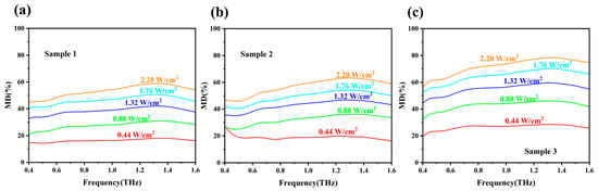
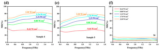
Figure 5.
Modulation depth diagrams of (a) Sample 1, (b) Sample 2, (c) Sample 3, (d) Sample 4, (e) Sample 5, and (f) bare Si under 532 nm laser excitation.
Figure 6.
Variation in the terahertz modulation depth of all samples with the pump laser power density at 1.3 THz.

Table 1.
Comparison of modulation performances of various terahertz modulators.
To determine the modulation mechanism of the samples, additional terahertz experiments on Cs2CuSbCl6/sapphire were conducted, and the results are shown in Figure 7. It can be observed that sapphire exhibits no modulation effect on terahertz waves, and the Cs2CuSbCl6/sapphire structure also shows no terahertz modulation capability. Sapphire has a band gap of 9 eV and acts as an insulator, which cannot form a heterojunction structure with Cs2CuSbCl6. Thus, the terahertz modulation of the Cs2CuSbCl6/sapphire structure would primarily be attributed to Cs2CuSbCl6 itself. However, the experimental results indicate that Cs2CuSbCl6 alone does not induce terahertz optical modulation. It is therefore evident that the modulation effect of the Cs2CuSbCl6/Si device originates primarily from the Cs2CuSbCl6/Si heterojunction.
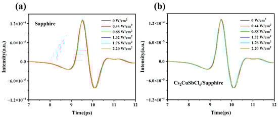
Figure 7.
Terahertz time-domain spectra (THz-TDS) of (a) sapphire and (b) Cs2CuSbCl6/sapphire under 532 nm laser pumping.
Figure 8 presents the absorption spectrum and Tauc plot of the Cs2CuSbCl6 nanocrystals. Both the absorption spectrum and the Tauc plot are consistent with the literature reports, further verifying the successful synthesis of the nanocrystals. Due to the weak absorption of the 532 nm pump laser by the Cs2CuSbCl6 film, based on the above analysis, the majority of photogenerated carriers are generated in the silicon substrate. Experimental observations reveal that under laser irradiation, the attenuation of the terahertz wave intensity transmitted through the Cs2CuSbCl6 thin-film sample is significantly higher than that through bare silicon materials. Combined with the analysis of steady-state conductivity and terahertz modulation trends, we infer that this phenomenon is associated with the enhanced carrier lifetime, and the relevant analysis is as follows:
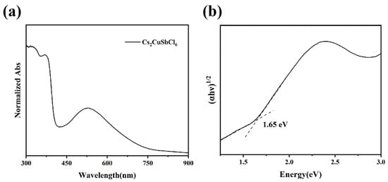
Figure 8.
(a) Absorption spectrum and (b) band gap diagram of Cs2CuSbCl6.
This phenomenon is most likely attributed to the heterojunction formed at the interface between the Cs2CuSbCl6 thin film and the silicon substrate. Given the Fermi level difference between the Cs2CuSbCl6 thin film and the silicon substrate, electrons are likely to migrate from the region with a higher Fermi level to that with a lower one, thereby potentially inducing carrier diffusion. Such diffusion may further lead to the formation of a space charge region and the generation of a built-in electric field. It is inferred that the presence of this built-in electric field can trigger carrier drift, and ultimately, a dynamic equilibrium may be established between diffusion and drift motions.
Consistent with the analysis of steady-state conductivity and terahertz modulation trends, our inference suggests that the diffusion and drift of electrons can extend the carrier lifetime, which in turn may enhance the terahertz modulation effect. Analysis indicates that the built-in electric field of the Cs2CuSbCl6/Si heterojunction can significantly facilitate carrier transport; furthermore, based on the inferences from steady-state conductivity and terahertz modulation trends, both carrier mobility and lifetime exhibit an increasing trend. This heterojunction structure is expected to optimize the overall device architecture and improve carrier transport behavior, thereby potentially enhancing the comprehensive performance of the device. Experimental tests demonstrate that the performance of the Cs2CuSbCl6/Si heterojunction device is approximately six times that of the bare silicon device.
To verify the above viewpoint and elaborate on the carrier transport mechanism in the samples, the band gap and vacuum level of Cs2CuSbCl6 were determined using absorption spectroscopy and photoelectron spectroscopy, and their heterojunction structure diagram was presented. The absorption spectrum and band gap diagram are shown in Figure 8, while the ultraviolet photoelectron spectroscopy (UPS) spectrum is illustrated in Figure 9. Based on the UPS data, the valence band maximum (EVBM) and secondary electron cutoff edge (Ecutoff) of Cs2CuSbCl6 were derived. Using the formula work function Φ = 21.22 − Ecutoff (where 21.22 eV corresponds to the photon energy of the He I excitation source in UPS), the work function of Cs2CuSbCl6 was calculated to be 3.91 eV.
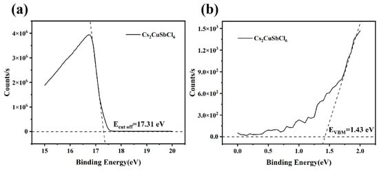
Figure 9.
(a) Secondary electron cutoff edge and (b) valence band maximum (VBM) of Cs2CuSbCl6.
Thus, the key energy level parameters of Cs2CuSbCl6 are summarized as follows: work function (Φ) = 3.91 eV, conduction band minimum (Ec) = −5.34 eV, valence band maximum (Ev) = −3.69 eV, Fermi level (Ef) = −3.91 eV, and band gap (Eg) = 1.65 eV. For bare silicon, the corresponding parameters are known to be Φ = 4.6 eV, Ec = −4.04 eV, Ev = −5.16 eV, Ef = −4.6 eV, and Eg = 1.12 eV. The vacuum level was set to 0 eV. Their energy level diagram and heterojunction structure diagram are shown in Figure 10.
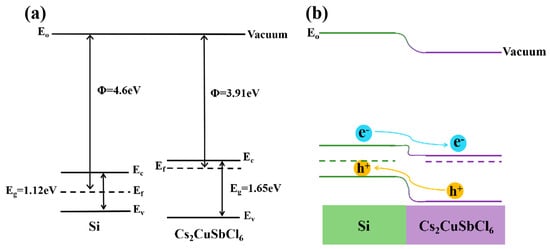
Figure 10.
(a) Energy level diagram and (b) heterojunction structure diagram of Cs2CuSbCl6.
As can be seen from the figures, the Cs2CuSbCl6 thin film forms a Type-II heterojunction with intrinsic silicon—this structure is conducive to the separation of photogenerated carriers. When the two materials are in contact, under thermal equilibrium, electrons initially migrate from Cs2CuSbCl6 to silicon until the Fermi levels of Cs2CuSbCl6 and silicon align, forming the heterojunction structure illustrated in Figure 10b. Under the influence of the built-in electric field, electrons are likely to flow from silicon to Cs2CuSbCl6, while holes tend to migrate from Cs2CuSbCl6 to silicon. This spatial separation of electrons and holes can enhance the polarizability of the sample to some degree, while concomitantly reducing the electron–hole recombination rate. Building on the analysis of steady-state conductivity and terahertz modulation trends, we deduce that this process can effectively extend the carrier lifetime. Meanwhile, the conductivity and dielectric constant of the sample are also expected to exhibit an upward trend. In light of the above inference, the refractive index and terahertz absorption rate of the sample are likely to increase correspondingly, and the terahertz modulation effect can be significantly optimized.
The relationship between the terahertz transmittance T(ω) and complex conductivity σ(ω) of the Cs2CuSbCl6/Si photoexcited layer is expressed as [18,19] , where σ denotes the complex conductivity of the sample, Z0 is the free-space impedance (Z0 = 377 Ω), N is the refractive index of the silicon substrate (N = 3.42), and d is the thickness of the photoexcited layer. Under 532 nm continuous-wave laser excitation, the penetration depth of silicon is approximately 1 μm [20], as shown in Figure 11.
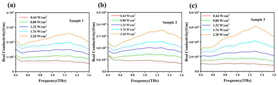
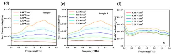
Figure 11.
Conductivity of (a) Sample 1, (b) Sample 2, (c) Sample 3, (d) Sample 4, (e) Sample 5, and (f) bare Si under 532 nm laser excitation.
Under laser irradiation, the conductivity of all samples increases significantly with the increase in laser power density, which is attributed to the enhancement of carrier concentration. Figure 12 presents the variation in sample conductivity at 1.3 THz with increasing pump power. At a laser power density of 2.2 W/cm2, the conductivity of Sample 4 reaches 8.4 × 10⁴ S/m, which is approximately 12 times that of bare silicon. Figure 13 illustrates the conductivity of different samples at 1.3 THz under a laser power density of 2.2 W/cm2. The conductivity of the samples first increases and then decreases with the rise in annealing temperature, reaching a peak at 180 °C—this trend is consistent with the variation in terahertz modulation depth reported earlier.
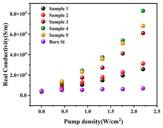
Figure 12.
Variation in the conductivity of all samples with the irradiated laser power density at 1.3 THz.
Figure 13.
Variation in the conductivity of the samples with annealing temperature at 1.3 THz under a laser power density of 2.2 W/cm2.
We speculate that the annealing temperature affects the compactness of the thin film and the number of interface defects. A dense thin film cannot be formed at lower annealing temperatures, resulting in a smaller contact area between Cs2CuSbCl6 and the silicon substrate, and thus an insignificant heterojunction effect. In contrast, higher annealing temperatures may induce more interface defects, which hinder carrier transport and mobility, thereby affecting carrier concentration and weakening the terahertz modulation effect of the samples.
In addition, it can be seen from the absorption spectrum that the absorption peaks of Cs2CuSbCl6 are mainly located in the high-frequency ultraviolet (UV) region. We speculate that better modulation performance will be achieved if ultraviolet light modulation is adopted. The electron–hole pair generation rate per unit time and unit area in Cs2CuSbCl6, denoted as N, can be expressed as [19] , where P represents the laser power, R is the reflectivity of the sample to the laser, S is the irradiated area, hν denotes the photon energy of the laser, and α is the absorption coefficient of Cs2CuSbCl6.
It can be inferred from this that the electron–hole pair generation rate of Cs2CuSbCl6 is higher under ultraviolet light, thereby resulting in a larger total number of photogenerated carriers. The average total number of photogenerated carriers can be expressed as , where n and p denote the number of electrons and holes, respectively; τ is the average lifetime of photogenerated carriers; and d is the effective thickness involved in optical modulation. As can be seen from the above formulas, the high absorption of high-frequency light by the sample leads to a higher carrier concentration, which in turn enhances the modulation depth.
4. Conclusions and Outlook
In summary, a novel Cs2CuSbCl6/Si terahertz modulator was fabricated in this work by spin-coating a Cs2CuSbCl6 thin film onto a pristine silicon substrate. A home-built terahertz time-domain spectrometer (THz-TDS) was employed to accurately measure the terahertz transmittance, modulation depth, and apparent electrical conductivity of the samples. Experimental results demonstrate that the Cs2CuSbCl6/Si modulator exhibits excellent terahertz modulation performance under pump laser irradiation. Specifically, at a laser power density of 2.2 W/cm2, the modulation depth of Sample 4 reaches 84%, which is 6 times that of bare silicon under the same conditions, greatly enhancing the modulation depth of silicon-based all-optical terahertz modulators.
The excellent modulation depth exhibited by this device may be associated with the Type-II heterojunction structure formed at the thin film–substrate interface. The strong built-in electric field at the interface could effectively separate photogenerated carriers and reduce the recombination rate of electrons and holes. Based on the analysis of steady-state conductivity and terahertz modulation trends, we infer that this process could extend the carrier lifetime, while the carrier concentration and mobility of the sample may also show an increasing trend—these properties may enhance the terahertz modulation effect of the sample to a certain extent. We speculate that if this modulator is applied in high-frequency ultraviolet (UV) fields in the future, it may exhibit better performance.
Supplementary Materials
The following supporting information can be downloaded at: https://www.mdpi.com/article/10.3390/opt7010005/s1. Figure S1: (a) SEM image of Sample 1; (b) SEM image of Sample 2; (c) SEM image of Sample 3; (d) SEM image of Sample 4; (e) SEM image of Sample 5; (f) SEM image of Sample 4.
Author Contributions
X.S.: visualization, writing—original draft. Z.Z.: supervision. R.T.: software. A.Y.: conceptualization, project administration. M.X.: resources, materials preparation. B.A.: funding acquisition, investigation. All authors have read and agreed to the published version of the manuscript.
Funding
This work was financially supported by Xinjiang Natural Science Foundation for General Program (No. 2023D01A40), Research Program of Xinjiang Higher Education (No. XJEDU2023J030), the National Natural Science Foundation of China (No. 22363011), Tianshan Talent Training Program of Xinjiang (No. 2024TSYCCX0064), University of Science and Technology of China–Xinjiang Normal University Counterpart Cooperation and Development Joint Fund (No. XJNULH2503).
Data Availability Statement
The original contributions presented in this study are included in the article. Further inquiries can be directed to the corresponding author.
Conflicts of Interest
The authors declare no conflicts of interest.
References
- Huang, Y.; Shen, Y.; Wang, J. From Terahertz Imaging to Terahertz Wireless Communications. Engineering 2023, 22, 106–124. [Google Scholar] [CrossRef]
- Li, S.; Zhang, F.; Han, Q.; Zhou, M.; Yan, L.; Tan, Y.; Li, X.; Li, A.; Abulimiti, B.; Li, Z.; et al. All-optical broadband terahertz modulator based on CdS NWs/Si heterojunction and interface photoconductivity analysis. Phys. Scr. 2024, 99, 115516. [Google Scholar] [CrossRef]
- Zhou, M.; Li, A.; Li, S.; Zhang, F.; Li, Z.; Jin, B. All-optical broadband terahertz modulator based on NiO/Si heterojunction and interface photoconductivity analysis. APL Mater. 2025, 13, 031119. [Google Scholar] [CrossRef]
- Jakhar, A.; Kumar, P.; Moudgil, A.; Dhyani, V.; Das, S. Optically Pumped Broadband Terahertz Modulator Based on Nanostructured PtSe2 Thin Films. Adv. Opt. Mater. 2020, 8, 1901714. [Google Scholar] [CrossRef]
- Zhang, P.; Liang, Q.; Zhou, Q.; Chen, J.; Li, M.; Deng, Y.; Liang, W.; Zhang, L.; Zhang, Q.; Gu, L.; et al. High-performance terahertz modulators induced by substrate field in Te-based all-2D heterojunctions. Light Sci. Appl. 2024, 13, 67. [Google Scholar] [CrossRef] [PubMed]
- Chen, S.; Jin, J.; Wang, W.; Wang, S.; Du, X.; Wang, F.; Ma, L.; Wang, J.; Wang, C.; Zhang, X.; et al. Thermally tunable anti-ambipolar heterojunction devices. Phys. Chem. Chem. Phys. 2024, 26, 23438–23446. [Google Scholar] [CrossRef] [PubMed]
- Shen, L.; Chen, R.; Zhang, D.; Yilmazoglu, U.C.; Gu, K.; Sarmiento, J.S.; Zhu, T.; Zheng, L.; Zheng, J.; Wang, H.; et al. High-Performance Perovskite Photovoltaics by Heterovalent Substituted Mixed Perovskites. Adv. Funct. Mater. 2022, 32, 2207911. [Google Scholar] [CrossRef]
- Case, C.; Beaumont, N.; Kirk, D. Industrial Insights into Perovskite Photovoltaics. ACS Energy Lett. 2019, 4, 2760–2762. [Google Scholar] [CrossRef]
- Gu, Y.; Du, H.; Li, N.; Yang, L.; Zhou, C. Effect of carrier mobility on performance of perovskite solar cells. Chin. Phys. B 2019, 28, 48802. [Google Scholar] [CrossRef]
- Manfo, T.A.; Yıldız, D.E.; Hussaini, A.A.; Yıldırım, M.; Gündüz, B. The light detection performance of the Al/DCJTB/n-Si Schottky type photodetector for a wide-range spectrum. Opt. Mater. 2026, 169, 117688. [Google Scholar] [CrossRef]
- Xiao, Z.; Song, Z.; Yan, Y. From Lead Halide Perovskites to Lead-Free Metal Halide Perovskites and Perovskite Derivatives. Adv. Mater. 2019, 31, 1803792. [Google Scholar] [CrossRef] [PubMed]
- Ahn, C.W.; Jo, J.H.; Chan Kim, J.; Ullah, H.; Ryu, S.; Hwang, Y.; San Choi, J.; Lee, J.; Lee, S.; Jeen, H.; et al. Highly ordered lead-free double perovskite halides by design. J. Mater. 2020, 6, 651–660. [Google Scholar] [CrossRef]
- Frenzel, M.; Cherasse, M.; Urban, J.M.; Wang, F.; Xiang, B.; Nest, L.; Huber, L.; Perfetti, L.; Wolf, M.; Kampfrath, T.; et al. Nonlinear terahertz control of the lead halide perovskite lattice. Sci. Adv. 2023, 9, eadg3856. [Google Scholar] [CrossRef] [PubMed]
- Zhou, W.; Han, P.; Zhang, X.; Zheng, D.; Yang, S.; Yang, Y.; Luo, C.; Yang, B.; Hong, F.; Wei, D.; et al. Lead-Free Small-Bandgap Cs2CuSbCl6 Double Perovskite Nanocrystals. J. Phys. Chem. Lett. 2020, 11, 6463–6467. [Google Scholar] [CrossRef] [PubMed]
- Elassib, H.; Alla, M.; Tourougui, S.; Alla, M.; Elfatouaki, F.; Dar, S.A.; Chauhan, A.; Naima; Chawki, N.; Shrivastav, N.; et al. High-performance optimization and analysis of Cs2CuSbCl6-Based lead-free double perovskite solar cells with theoretical efficiency exceeding 27%. Renew. Energy 2025, 239, 12092. [Google Scholar]
- Soni, Y.; Rani, U.; Shukla, A.; Joshi, T.K.; Verma, A.S. Transition metal-based halides double Cs2ZSbX6 (Z = Ag, Cu, and X = Cl, Br, I) perovskites: A mechanically stable and highly absorptive materials for photovoltaic devices. J. Solid State Chem. 2022, 314, 123420. [Google Scholar] [CrossRef]
- Shi, Y.; Zhou, Q.; Zhang, C.; Jin, B. Ultrafast high-field carrier transport in GaAs measured by femtosecond pump-terahertz probe spectroscopy. Appl. Phys. Lett. 2008, 93, 121115. [Google Scholar] [CrossRef]
- Cao, Y.; Gan, S.; Geng, Z.; Liu, J.; Yang, Y.; Bao, Q.; Chen, H. Optically tuned terahertz modulator based on annealed multilayer MoS2. Sci. Rep. 2016, 6, 22899. [Google Scholar] [CrossRef] [PubMed]
- Peter, U.J.; David, G.C.; Martin, K. Terahertz spectroscopy and imaging- Modern techniquesand applications. Laser Photonics Rev. 2011, 5, 124–166. [Google Scholar]
- Simona, B.; Alessia, L.D.; Andrea, R.; Beat, J.; Beat, N.; Chiara, B.; Cesare, F.; Davide, S.; Luca, L.; Sergio, P. Picosecond laser texturization of mc-silicon for photovoltaics: Acomparison between 1064 nm, 532 nm and 355 nm radiationwavelengths. Appl. Surf. Sci. 2016, 371, 196–202. [Google Scholar]
Disclaimer/Publisher’s Note: The statements, opinions and data contained in all publications are solely those of the individual author(s) and contributor(s) and not of MDPI and/or the editor(s). MDPI and/or the editor(s) disclaim responsibility for any injury to people or property resulting from any ideas, methods, instructions or products referred to in the content. |
© 2026 by the authors. Licensee MDPI, Basel, Switzerland. This article is an open access article distributed under the terms and conditions of the Creative Commons Attribution (CC BY) license.