Article

Characterization of Boron Coatings Produced by RF Planar Magnetron Sputtering

1
Institute for Plasma Science and Technology (ISTP), National Research Council (CNR), Via R. Cozzi 53, 20125 Milan, Italy
2
Institute of Condensed Matter Chemistry and Technologies for Energy (ICMATE), National Research Council (CNR), Via R. Cozzi 53, 20125 Milan, Italy
3
Center for Sensors and Devices, Fondazione Bruno Kessler (FBK), Via Sommarive 18, 38123 Trento, Italy
4
Department of Industrial Engineering, University of Trento, Via Sommarive 9, 38123 Trento, Italy
5
Institute for Photonics and Nanotechnologies (IFN), National Research Council (CNR), Via alla Cascata 56/C, 38123 Trento, Italy
*
Author to whom correspondence should be addressed.
Surfaces 2026, 9(2), 31; https://doi.org/10.3390/surfaces9020031
Submission received: 24 February 2026 / Revised: 16 March 2026 / Accepted: 20 March 2026 / Published: 26 March 2026
(This article belongs to the Special Issue Surface Engineering of Thin Films)

Abstract

Boron coatings were deposited by RF magnetron sputtering in an Ar atmosphere at a constant power of 80 W, varying the working pressure in the 0.6–5 Pa range. Plasma diagnostics were performed by means of a Langmuir probe to determine the electron temperature and electron density under different operating conditions. Within the investigated pressure range, the deposition rate remained nearly constant, whereas a significant decrease in coating mass density was observed with increasing pressure. The coatings display a columnar structure at all investigated pressures, with no significant differences in bulk morphology. Pressure primarily affects the surface features, leading to an increase in the density, lateral dimensions, and height of surface agglomerates with increasing pressure. Compositional analysis by EDX revealed a substantial oxygen incorporation in the films, with the lowest oxygen content (~11 at.%) measured for the coating deposited at 0.6 Pa. XPS depth profiling confirmed the presence of oxygen and evidenced the formation of boron oxide species, while the boron concentration exceeded 80 at.% in all samples. These results highlight the strong sensitivity of boron film density and oxygen uptake to sputtering pressure.

1. Introduction

Boron (B) coatings play a crucial role in a wide range of industrial applications owing to their distinctive properties. In general, the term ‘B coatings’ refers to boron-based coatings, such as boron nitride and boron carbide, among others. These coatings significantly enhance the surface properties of materials, providing high hardness, toughness, corrosion resistance, and wear resistance [1,2,3]. Nevertheless, pure B coatings also exhibit specific properties that make them attractive for certain industrial applications. In particular, thin pure B coatings can be used as protective layers on the walls of thermonuclear fusion facilities, mainly to reduce plasma impurities and improve plasma confinement [4,5]. B films find application as components in electronic devices due to their semiconducting or insulating properties, as well as their high thermal stability [6,7], and as two-dimensional (2D) materials in optical devices [8,9]. Therefore, it is essential to investigate the characteristics of pure B coatings deposited using different technologies and to understand the relationship between these characteristics and the process conditions that led to their formation. B coatings can be deposited by chemical [10,11] and physical vapour deposition technologies. Each technology has its peculiarities, advantages, and disadvantages. Clearly, for environmental considerations, PVD methods are the better choice, as they produce less chemical waste and offer cleaner, safer processes. B films have been deposited using thermionic vacuum arc technology [12]; however, this method has the inherent drawback of cathode degradation caused by intense heat and arc erosion. Additionally, arc evaporation can sometimes result in the inclusion of droplets or particulates in the deposited film. Electron beam evaporation [13] and pulsed laser deposition (PLD) [14] have also been employed, but both face significant limitations in terms of industrial-scale scalability. In particular, achieving uniform film thickness on large substrates remains a challenge. Among the most common methods for producing boron-containing coatings are various low-pressure plasma discharges, particularly magnetron sputtering (MS). In MS, the cathode material is sputtered by ions generated in the plasma by energetic electrons, and the sputtered atoms then condense on the substrate. When using boron as the target material, a radio-frequency magnetron sputtering (RFMS) system is typically employed (usually at 13.56 MHz) since boron is a poor electrical conductor. Most studies involving RFMS focus on reactive magnetron sputtering processes to deposit boride and boron nitride thin films [15,16], or boron oxide films [17]. In contrast, very few articles address the sputtering of pure B targets to produce B coatings [18], mainly due to the difficulty of obtaining nearly pure B coatings as a result of boron’s strong affinity for oxygen, which leads to the formation of oxides. Even trace amounts of oxygen or water vapour in the sputtering chamber can result in the formation of boron oxides. The substrate itself may also act as a source of oxygen during boron growth; therefore, prior to boron deposition, the Si substrate was coated in the sputtering chamber with a metallic tungsten layer.
To the best of our knowledge, no experimental studies on the deposition of boron films under conditions comparable to ours have been reported in the literature. However, for comparison purposes, reference can be made to boron coatings deposited using different techniques. In the work of Mijatovic et al. [19], the oxygen content, determined by XPS, in boron films grown by PLD was found to be critically dependent on the purity of the ambient gas. In particular, they demonstrated that the oxygen detected in the coating mainly originated from the background atmosphere in the chamber. Operating at a process pressure of approximately 20 Pa, they reported an oxygen content of about 11 at.% when using argon with a purity of 99.9999%, whereas reducing the gas purity to 99.995% resulted in more than a twofold increase in oxygen concentration. Similarly, Dellasega et al. [14], also using PLD, reported an oxygen content of approximately 11 at.% in boron coatings deposited at a significantly lower pressure (0.0005 Pa). They attributed this oxygen incorporation to the oxygen present in the target material and, to a lesser extent, to the residual atmosphere in the deposition chamber.
This study aims to clarify how sputtering pressure affects plasma conditions and the resulting microstructure, density, and oxygen uptake of boron thin films. We investigate B coatings deposited by RF magnetron sputtering in an Ar atmosphere as a function of the process pressure (0.6–5 Pa). The films were characterized from a morphological point of view by scanning electron microscopy (SEM) and atomic force microscopy (AFM), and their elemental composition was analyzed by energy-dispersive X-ray spectroscopy (EDS) and X-ray photoelectron spectroscopy (XPS). In addition, in order to understand possible relationships between plasma and process parameters and the resulting coating structure, the electron temperature (Te) and electron density (ne) were also estimated using a Langmuir probe (LP) [20,21].

2. Materials and Methods

2.1. Materials

Silicon (Si) substrates, chosen for their perfectly flat surfaces, were used to characterize the morphology, deposition rate, and mass density, enabling the detection of minor differences in deposit structure without interference from substrate roughness (Si, p-type (100), 1 cm × 1 cm, thickness of 400 microns, average roughness ≈ 1 nm). Argon (grade 5.0, 99.999% purity) gas was a Sapio Group (Monza, Italy) product.

2.2. Experimental Apparatus

The plasma system [22] consists of a cylindrical stainless-steel vacuum chamber with a volume of 0.05 m3, equipped with balanced-type magnetron sputtering cathodes (Angstrom Sciences, Duquesne, PA, USA). The cathodes are water-cooled and connected to an independent radio-frequency power supply (ωrf/2π = 13.56 MHz, 300 W; TRUMPF Hüttinger, Ditzingen, Germany) operating in steady-state mode and coupled with an automatic impedance matching unit to minimize reflected power. Boron (B) and tungsten (W) targets (diameter: 76.2 mm; purity: 99.9%; thickness: 6.35 mm) were mounted on the working cathode and powered at 80 W (power density ≈ 1.7 W/cm2). The sputtering time was fixed at 180 min. The stainless-steel substrate holder, positioned opposite the target, was designed to float electrically, allowing the application of a bias. An argon plasma was generated at a constant flow rate of 20 sccm under different operating conditions. The sputtering process pressure was controlled by partially closing a throttle valve between the vacuum chamber and the turbopump. The Ar flow rate and working pressure were monitored using a mass flow controller (MKS instruments, Andover, MA, USA) and a capacitive vacuum gauge (Pfeiffer CMR 365, Pfeiffer, Aßlar, Germany), respectively. The sputtering chamber was evacuated by a high-vacuum pumping system consisting of a rotary pump (TRIVAC 24 m3/h, Leybold, Cologne, Germany) and a turbomolecular pump (TURBOVAC 150 L/s, Leybold, Cologne, Germany), achieving a base pressure of 1 × 10⁻⁴ Pa. Samples were placed on the lower electrode (sample holder), maintained at the floating potential in all experiments. The target-to-substrate distance was 120 mm.

2.3. Plasma Diagnostics

A Langmuir probe (Hiden ESPION, Warrington, UK) was employed to characterize the plasma parameters under different operating conditions. Measurements were carried out at a distance of approximately 80 mm from the target, in a region where the magnetic field was negligible. The probe consisted of a tungsten tip with a diameter of 0.1 mm and a length of 15 mm. The probe has a compensation circuit in order to minimize the RF interference with the measured probe signal [23]. Plasma parameters, such as electron density (ne) and electron temperature (Te), were determined from five consecutive scans, and the averaged current–voltage (I–V) characteristic curve was obtained using a semi-automatic data analysis procedure. The I–V curves were recorded by sweeping the Langmuir probe bias voltage between ±40 V. The probe tip was cleaned after each measurement by applying 30 V for 100 ms.
Since sputtering processes typically involve non-equilibrium (non-Maxwellian) plasmas, the Druyvesteyn method [24,25,26] was employed to directly determine the electron density (ne) and electron temperature (Te), independently of the shape of the electron energy distribution function (EEDF).

2.4. Mass Density (ρ) Measurements

The ρ of the B coatings was estimated by weighing the Si wafer before and after the B deposition (∆m) on a balance accurate at least to the nearest 10−5 g (Sartorius Göttingen, Germany, model: SECURA225D-1S). As the coating thickness (d) was known due to the surface profilometer characterization, the coating density was found from the formula:
ρ = ∆m/(d · A),   A = Si wafer area

2.5. Characterization of Coatings

Boron coatings were deposited on Si substrates without intentional heating of the sample holder. The thickness of the deposited films was determined by partially masking the substrates with a silicon mask during deposition. After mask removal, the step height between the coated and uncoated regions was measured using a P15 surface profiler (KLA Tencor, San Jose, CA, USA).
The morphological features of the samples were investigated by atomic force microscopy (AFM; Core AFM, Nanosurf GmbH, Langen, Germany) operated in dynamic mode, and by high-resolution scanning electron microscopy (SEM; Tescan MIRA III, Brno, Czech Republic). AFM measurements were performed under ambient conditions using Dyn190Al probes (force constant: 28–75 N/m; tip radius: 10 nm). For each sample, three AFM images over a scan area of 30 μm × 30 μm were acquired to evaluate the surface roughness (Ra).
The elemental composition of the boron coatings was analyzed by energy-dispersive X-ray spectroscopy (EDX). Measurements were performed at three different locations on the coating surface to ensure the reliability and uniformity of the compositional data. The analyses were carried out using a high-resolution scanning electron microscope (SEM; Hitachi SU70, Hitachi High-Technologies, Minato-ku, Tokyo, Japan) equipped with a NORAN 6 EDX system (Thermo Scientific, Waltham, MA, USA). To minimize the interaction volume and accurately determine the coating composition without interference from the underlying substrate, the electron beam was operated at an accelerating voltage of 5 kV.
Depth profiling of the chemical composition of the deposited boron film was performed using an Axis Ultra XPS spectrometer (Kratos, UK). The instrument was calibrated against the Au 4f7/2 core-level peak of a polycrystalline Au foil, fixed at a binding energy of 84.00 eV. Depth profiling was carried out using an Ar+ ion gun operated at an accelerating voltage of 4.8 kV. An ion current of 20 mA and a 3 × 3 mm2 raster area were selected to ensure uniform sputtering over a sufficiently large analysis region. Control of the correct spectra alignment on the BE scale was carried out, ensuring that the fitting components assigned to hydrocarbon contamination CHx and the graphitic C=C carbon were located respectively at 284.8 eV and 284.3 eV.
Wide survey spectra were acquired at the beginning and at the end of the depth profile with a pass energy of 160 eV. High-resolution spectra of the B1s, O1s, W4f, N1s, and C1s core levels were collected using a pass energy of 20 eV and an energy step of 0.05 eV to ensure accurate reproduction of the spectral features. Shirley background subtraction and Voigt line shapes were applied for peak fitting and chemical state assignment. The evolution of the core-level line shapes throughout the depth profile was analyzed to evaluate changes in the chemical composition of the deposited film as a function of depth. Data analysis was performed using a custom software (RxpsG_3.3TK) package developed on the R platform [27].

3. Results

3.1. Plasma Characterization

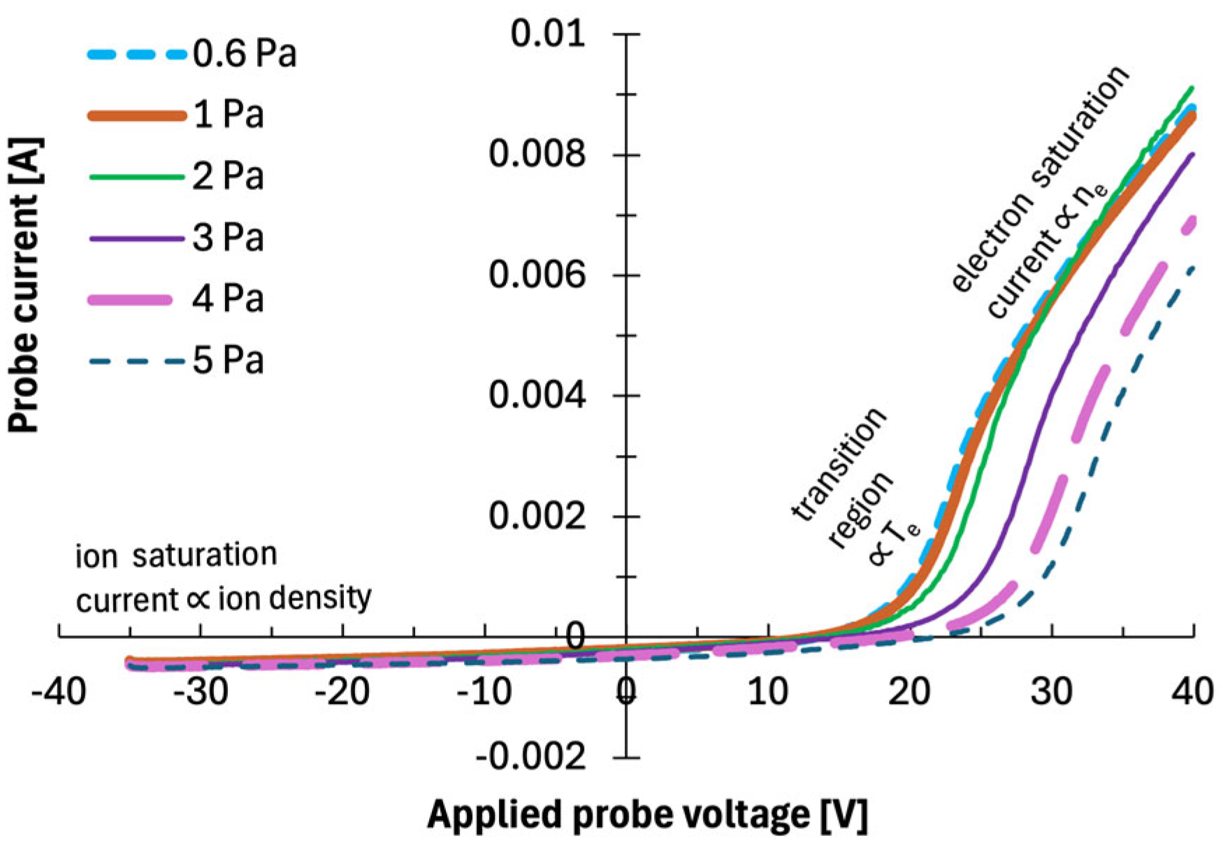
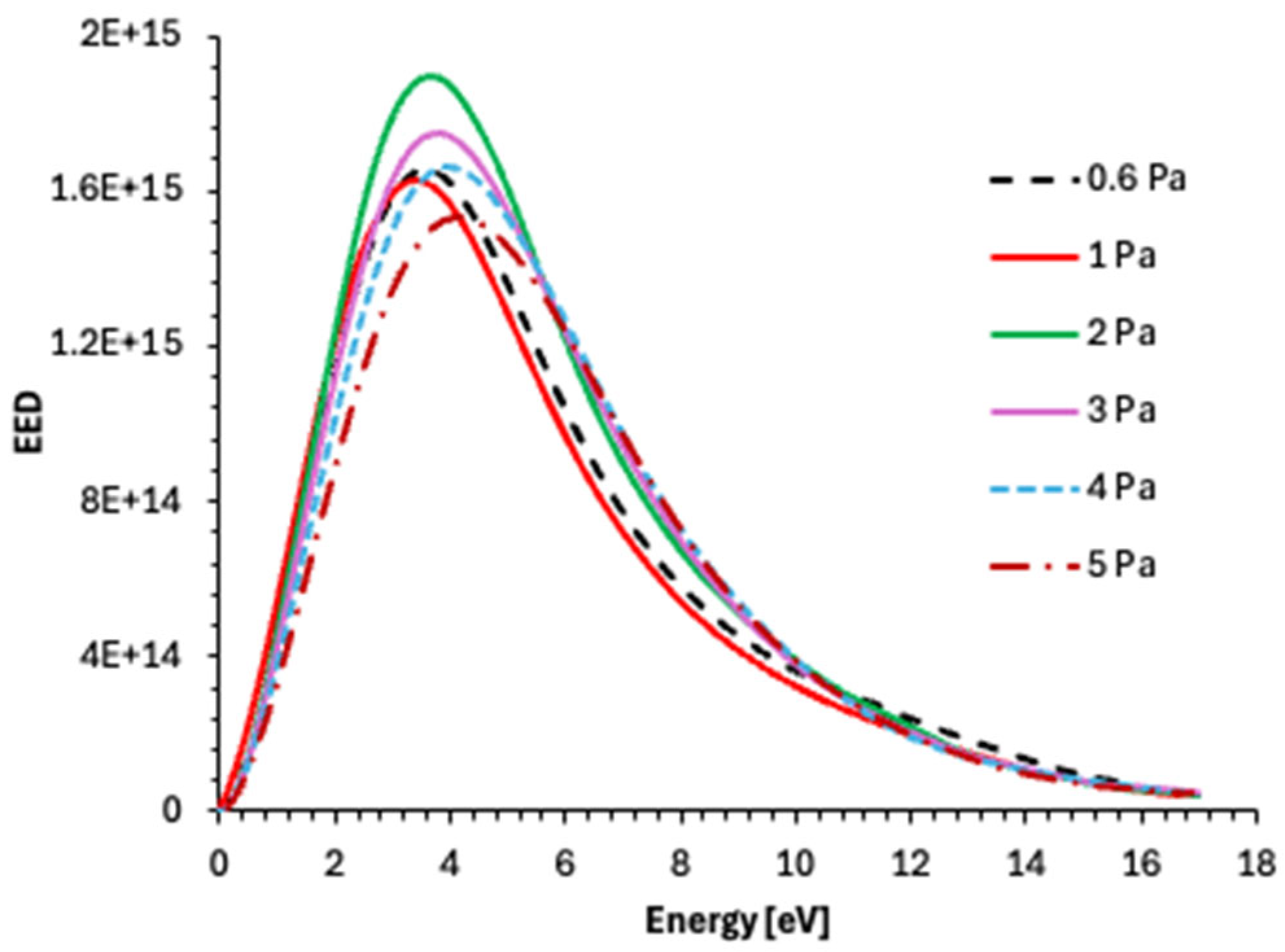
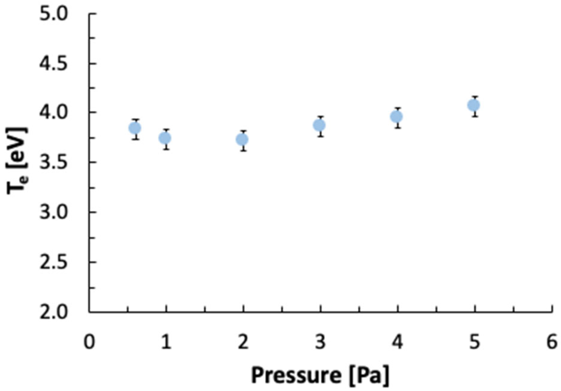
Probe measurements consisted of determining the current–voltage (I–V) characteristics of the probe, i.e., the dependence of the current in the probe circuit on the probe voltage relative to the reference electrode (in this case, the grounded vacuum chamber). Figure 1 shows the probe I–V curves measured at a magnetron discharge power of 80 W as a function of pressure (corresponding to the deposition conditions of the B coatings). A rightward shift in the I–V curve was observed with increasing pressure. However, the slope of the curves in the exponential transition region and the electron saturation region varied only slightly; therefore, only minimal variation in the electron temperature (Te) and electron density (ne) is expected. Using Druyvesteyn’s method [25], the electron energy distribution functions (EEDFs) were obtained from the I–V characteristics (Figure 2). All EEDFs follow a Druyvesteyn distribution, as expected for magnetron discharges [28]. Within the analyzed pressure range, the plasma dynamics appear unchanged, as indicated by the measurements of Te and ne. The Te and ne profiles obtained from the processing of the EEDFs are shown in Figure 3 and Figure 4. Figure 3 shows that Te remains approximately constant, varying in the range of 3.7–4 eV depending on the pressure considered. As is well known, Te is primarily governed by the balance between electron heating (due to the electric field) and electron energy loss processes, mainly through inelastic collisions with neutral atoms or molecules. Therefore, these results suggest that within this pressure range, the electron mean free path and collision frequency adjust so that the electron energy distribution and effective electron temperature reach a quasi-steady state [29,30]. This is supported by the analysis of the EEDFs (Figure 2); the shape of the EEDFs does not change substantially, and examining the high-energy tail (>10 eV) shows that the most energetic electrons are not significantly affected by the increase in pressure. This may indicate that most of the electrons reaching the probe do not lose significant energy in collisions, and therefore, the electron temperature and density remain similar, as the more energetic electrons dominate the probe measurement. These energetic electrons are not significantly thermalized by collisions with neutral particles.
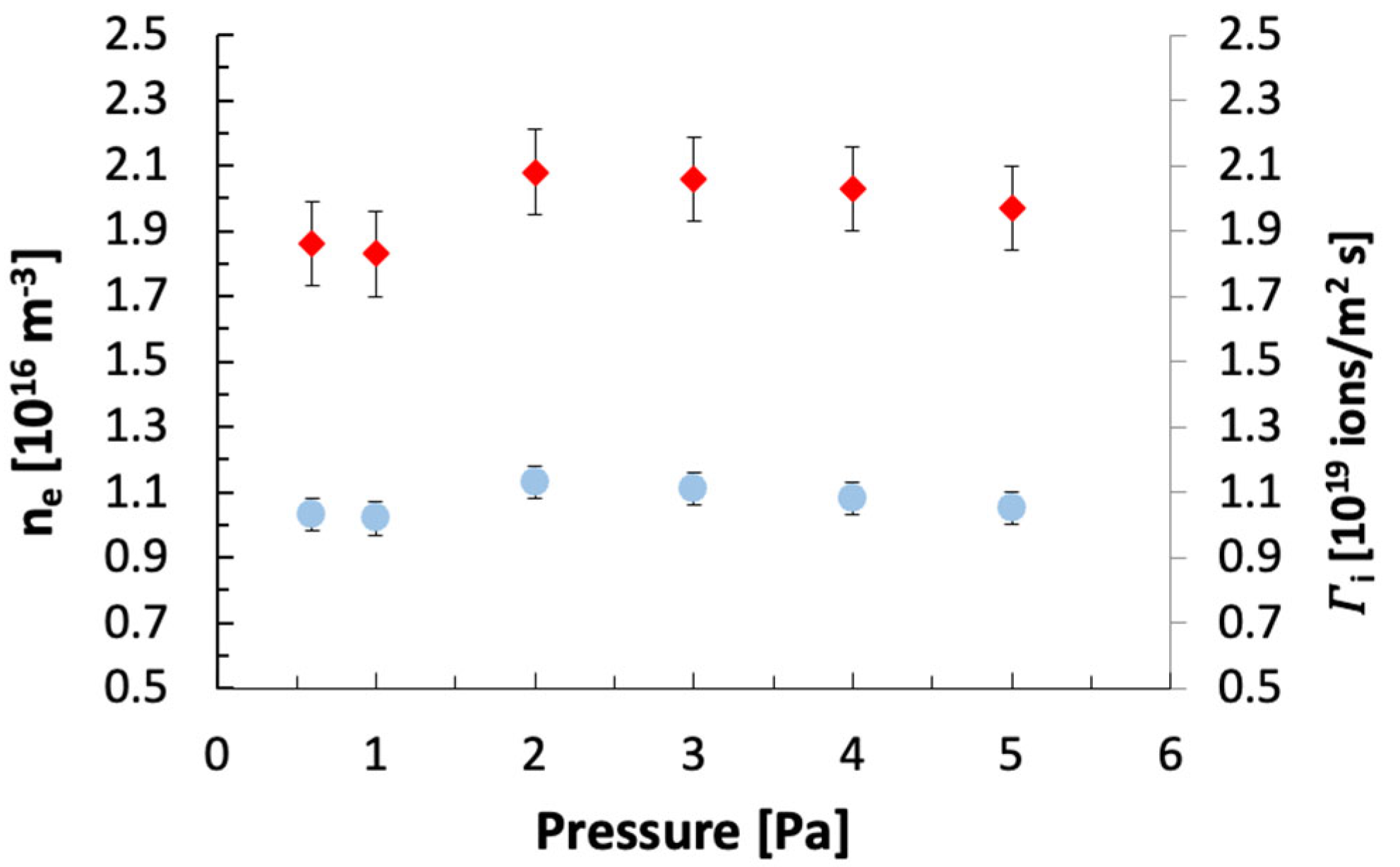
The same applies to the density, which remains at a value around 1.1 × 10¹⁶ m−3 and does not vary significantly over the pressure range considered, as shown in Figure 4.
Assuming quasi-neutrality ( n e n i ), the ion flux (Figure 4) was estimated using the Bohm criterion [31]. The ion flux (Γi) is only weakly affected by pressure, varying from 1.9 to 2.1 × 10¹⁹ ions m−2 s−1 across the investigated pressure range. Therefore, although the ion flux reaching the target plays a crucial role in determining the sputtering rate (SR) of the B target, it does not appear to significantly influence the structural growth of the deposited coatings. Consequently, as will be discussed in the following section, the structural properties of the B coatings are mainly determined by the flux of sputtered atoms arriving at the substrate, including their kinetic energy and scattering processes in the gas phase.

3.2. Coating Deposition

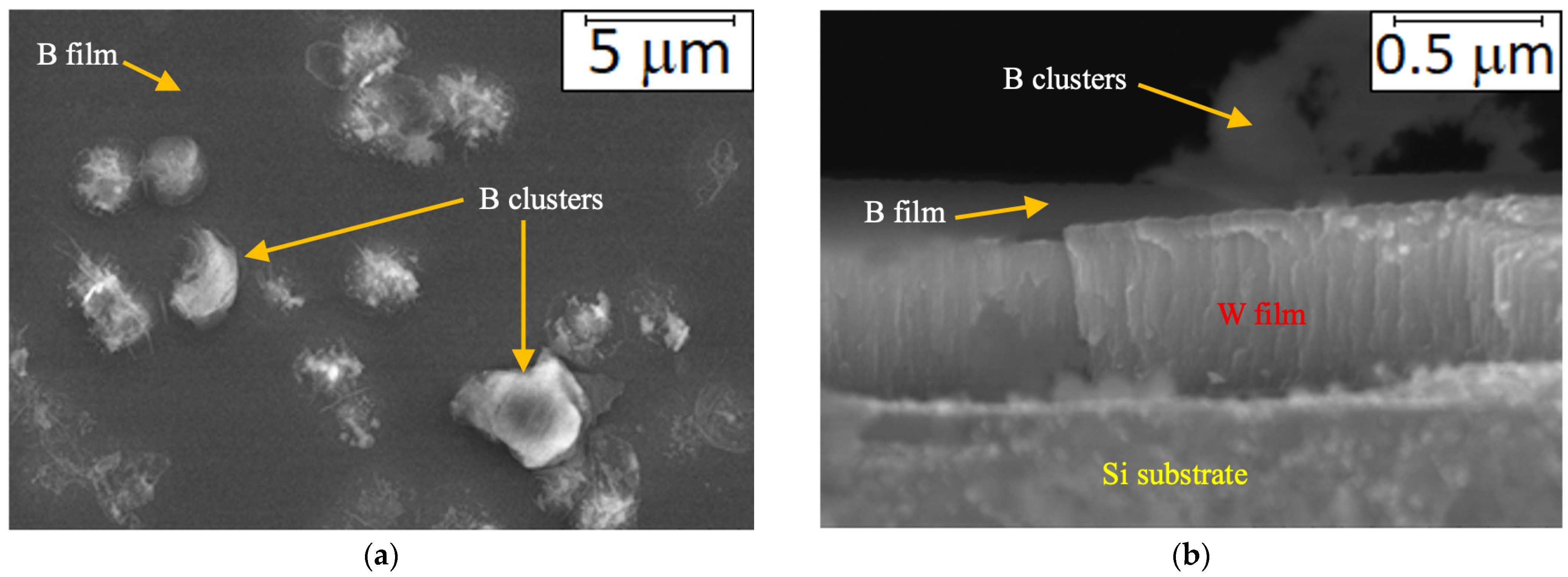
B coatings were deposited to investigate the effect of sputtering pressure (in the range of 0.6–5 Pa) on the deposition rate (DR), film density (ρ), and morphology. With regard to process pressure, pressures up to 4–5 Pa were explored; however, at these higher pressures, it was not possible to reliably measure DR or ρ, since the boron growth mechanism differs from that of conventional thin-film deposition. Boron coatings deposited by sputtering can form clusters under certain conditions [32], a phenomenon associated with several factors related to both the sputtering process and the intrinsic properties of boron. At pressures of 4–5 Pa, collisional effects significantly reduce the kinetic energy of B atoms, preventing sufficient surface diffusion to form a uniform coating. As a result, boron tends to aggregate both as a discontinuous film and as agglomerated clusters. It should also be noted that gas-phase generation of B clusters (or boron oxides) is likely, particularly at high pressures [33]. The formation of B clusters is detrimental to the deposition of a boron coating. This is because the clusters are highly reactive and, in particular, react with the atmosphere upon exposure to air (these clusters quickly form boron oxides and hydroxides), causing poor adhesion of coating, cracks, and coating failure (delamination) [34]. It should also be noted that a low-pressure vacuum chamber can act as a source of residual oxygen—a well-known phenomenon in vacuum-based processes—due to the outgassing of internal surfaces that adsorb gases when exposed to the atmosphere. Another factor we consider as a possible source of oxygen is the purity of the argon gas. As mentioned in the Introduction, since the sputtering gas used in this work has a purity of 99.999%, the residual oxygen present in the gas cylinder may play a role comparable [14,19] to that of residual water vapour released from the materials of the deposition chamber. Figure 5 shows the morphology of the B coating deposited on Si substrates (with a W interlayer) at 5 Pa. The formation of a boron structure consisting of both a thin film and clusters can be observed. Cluster formation was detected even at relatively low pressures, around 3 Pa. Therefore, under our experimental conditions, no cluster formation was observed at pressures of 2.4 Pa or lower, and the study was conducted within this pressure range. Moreover, the coating did not exhibit any signs of immediate delamination upon removal from the deposition reactor.
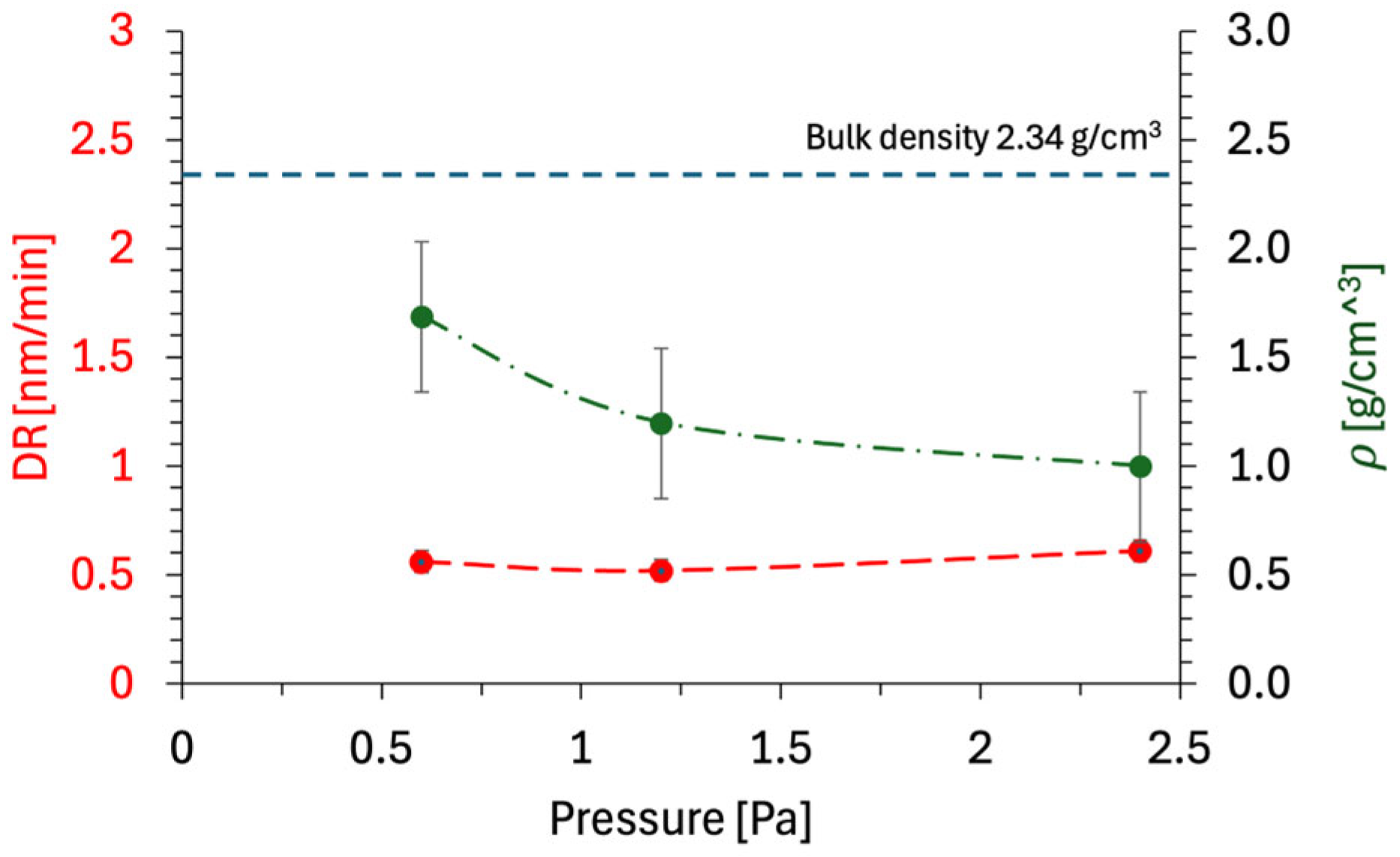
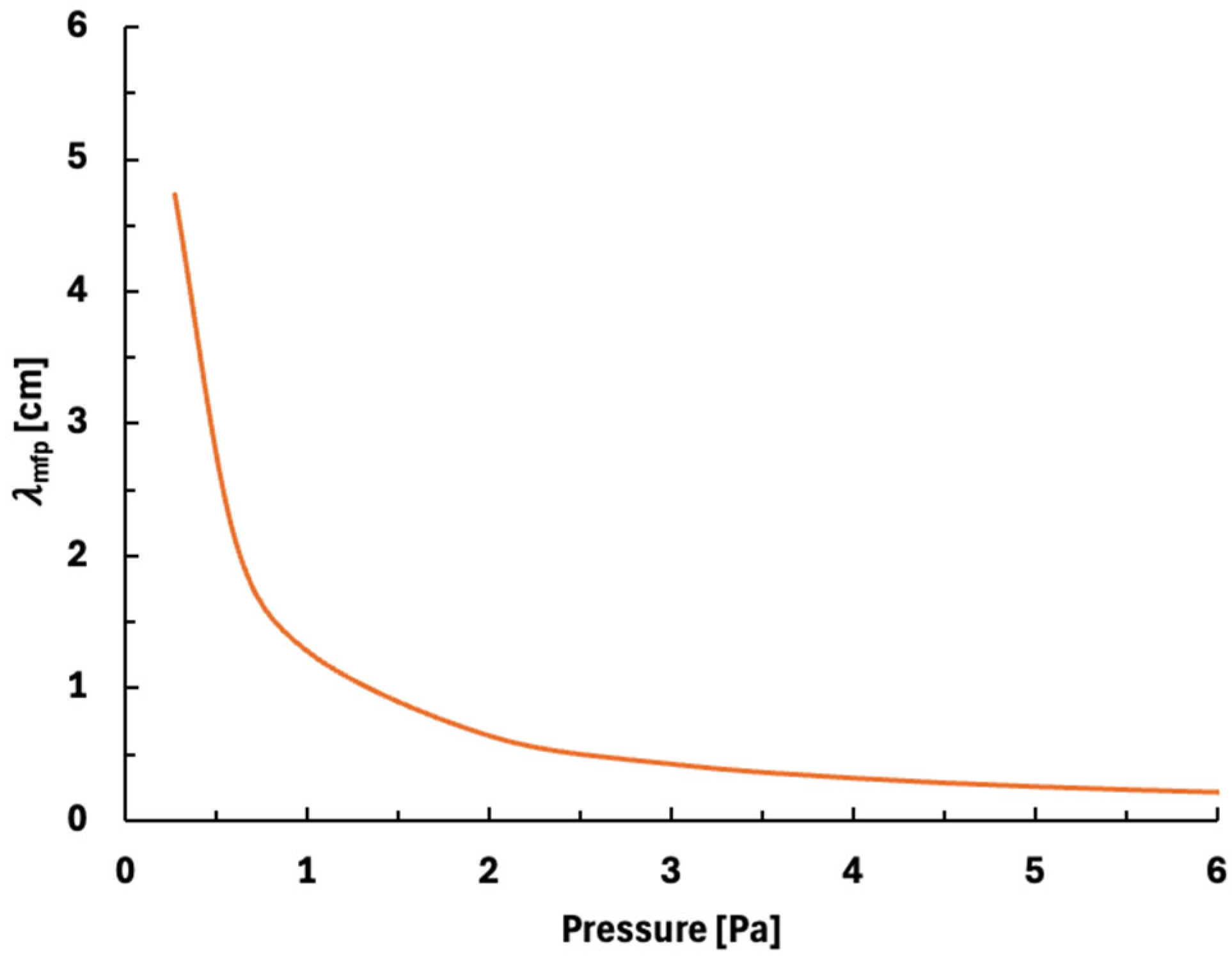
The deposition rate (DR) and film density (ρ) were analyzed as a function of sputtering pressure (Figure 6) while keeping the power constant. The DR did not change significantly over the pressure range considered. This result can be explained by noting that at lower pressures, fewer collisions compensate for the reduced ionization (see ne as a function of sputtering pressure in Figure 4). At higher pressures, the increased ion flux offsets scattering losses. Therefore, the balance between sputtering and transport remains relatively stable within this pressure range. In contrast, the ρ showed a clear dependence on pressure. At low pressures, the mean free path of sputtered atoms (Figure 7) increases, allowing them to travel directly to the substrate with minimal scattering and, consequently, limited energy loss. As a result, adatoms reach the substrate with higher kinetic energy, promoting the formation of denser coatings. As expected, the highest density (~1.7 g/cm3) was obtained at 0.6 Pa, although it remains lower than that of bulk boron (~2.3 g/cm3). Conversely, ρ decreases at higher pressures due to the increased scattering and energy loss of sputtered atoms. Similar density values were reported by Yushkov et al. [35].
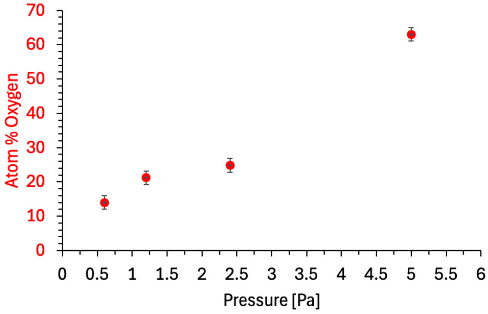
An important aspect to be evaluated in the deposition of B coatings is the amount of oxygen that B can incorporate (“capture”) [36]. B has a strong affinity for oxygen and readily forms stable oxides (such as boron oxide, B2O3), enabling it to effectively scavenge oxygen. In vacuum processes, B can therefore contribute to maintaining an oxygen-free environment by reacting with residual oxygen. Even when the sputtering gas does not contain oxygen, this contaminant is commonly present in the residual atmosphere of the sputtering chamber [37] and may be incorporated into the growing film during deposition. In sputtering systems, the presence of residual oxygen is a common phenomenon due to outgassing from internal surfaces. In fact, the chamber walls, holders, shields, and targets absorb oxygen, particularly water vapour, when the system is exposed to the atmosphere [38]. During the sputtering process, these gases are released and become an indirect source of oxygen. In order to evaluate the variation in oxygen content in the coatings as a function of the process pressure, the EDX technique was employed. Although this technique is significantly more sensitive to heavy atoms such as W than to light elements such as C and O, the oxygen concentration was determined semi-quantitatively (Figure 8), taking into account a possible error of up to 10–15%. Before focusing on the EDX analysis, several considerations should be addressed. All coatings were deposited at a base pressure of 10−4 Pa (after 24 h of pumping). EDX analysis was performed immediately after the deposition process; however, the samples were exposed to air for approximately 2 h. Moreover, no chamber degassing procedure was carried out prior to the sputtering process. Therefore, assuming a similar atmospheric environment for all the samples, the variation in oxygen in the coating (gettered O2) can be attributed to the amount of oxygen outgassed from the chamber materials (except for a few nm of surface oxidation). Returning to EDX measurements (Figure 8), varying the pressure produces a significant impact on film composition as regards the amount of oxygen (at.%). At 0.6 Pa, a minimum value of gettered oxygen was obtained (≈13 ± 2 at.%). Taking as a reference one of the applications of pure boron thin films (≈100 nm), such as boronization in tokamaks, where large vacuum chambers that are not thermally outgassed are used, the amount of gettered oxygen (at.%) at a pressure of ≈1 Pa is similar to that found in this experimental study [39]. The EDX data indirectly confirm that a higher amount of residual oxygen is present as the pressure increases, also taking into account that the coating density has decreased.
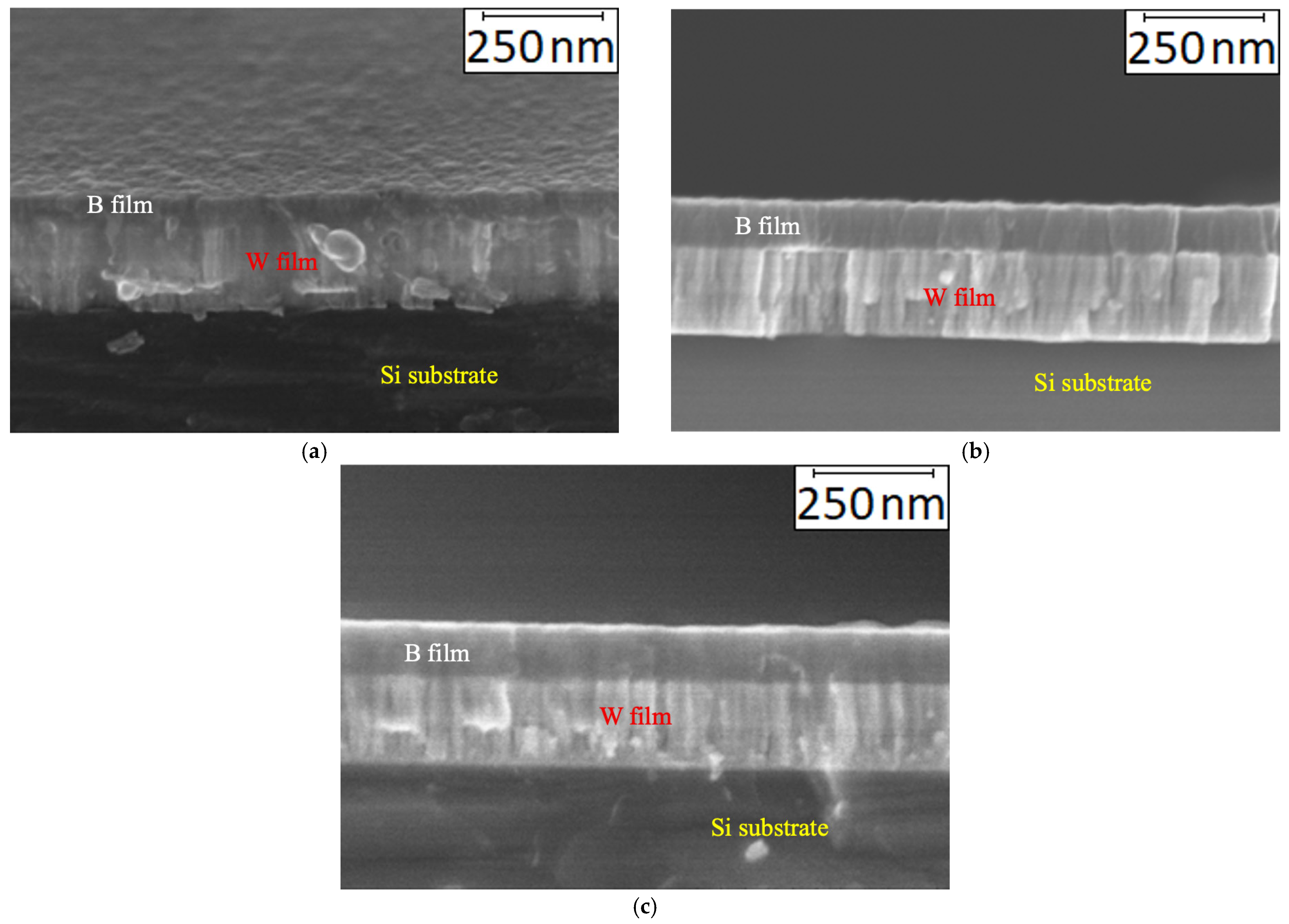
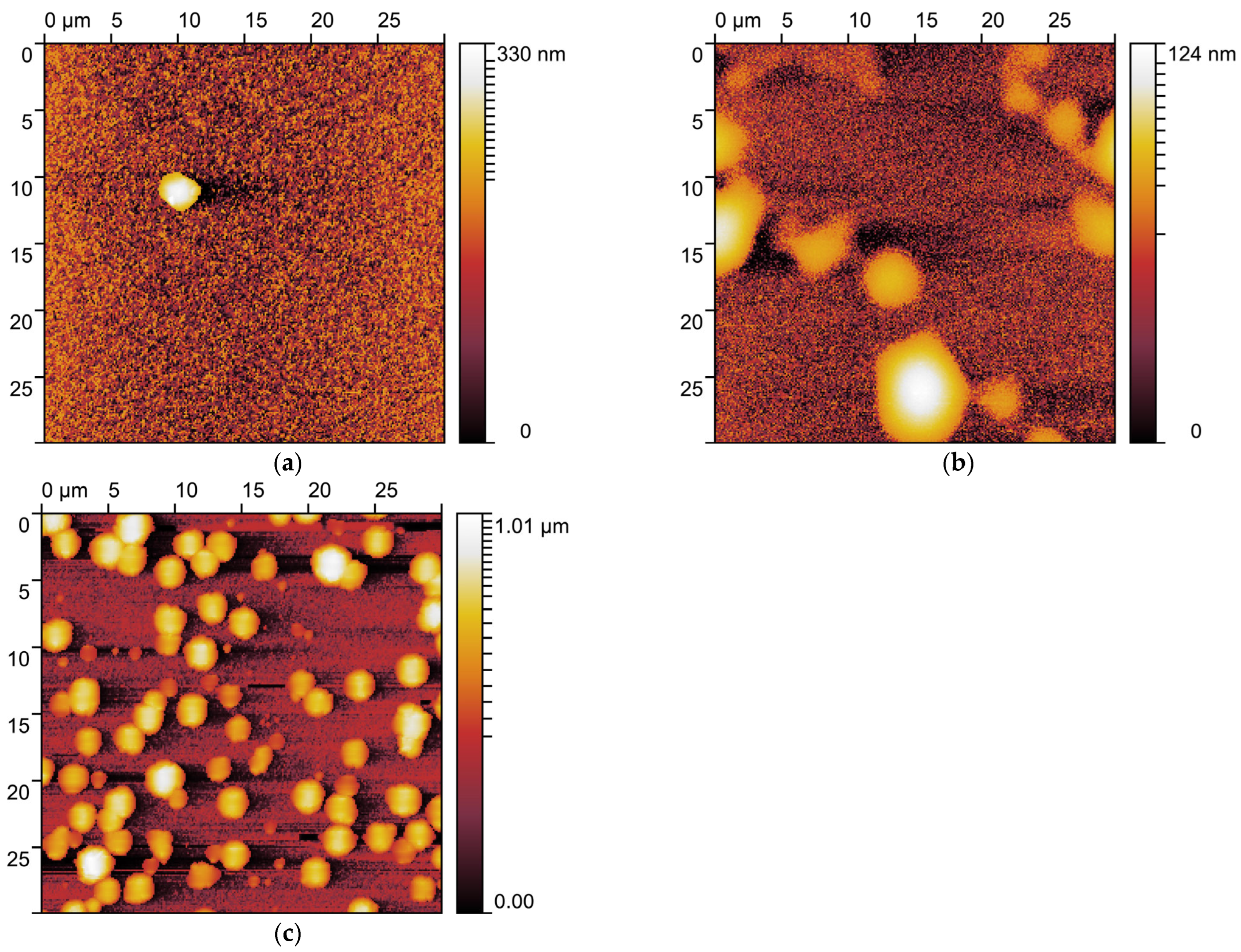
Figure 9 shows SEM cross-sectional micrographs of B coatings deposited at different pressures on a Si substrate with a W interlayer. In all samples, the W layer exhibits a columnar structure, and the subsequent B layer grows conformably on this underlying structure (as clearly shown in Figure 9, in particular, in (a) where the sample is shown slightly tilted). This is a clear indication that B atoms have relatively low surface mobility in this pressure range at 80 W of RF power. Consequently, they may not possess sufficient energy to diffuse across the W surface and form a relatively dense coating. As confirmed by the coating density measurements (Figure 6), the density is lower than that of the bulk material. Examining the cross-section of the coatings grown under varying process pressures, no significant structural differences are observed. The only notable morphological variation is on the surface of coatings. This is highlighted by the AFM measurements (Figure 10). Flat regions composed of agglomerates of varying sizes are observed on the surface. At 0.6 Pa (Figure 10a), an average of one agglomerate is observed within an area of 30 × 30 µm2, ranging in size from 2 to 3 µm. At 1.2 Pa (Figure 10b), several agglomerates appear, ranging in size from 2 to 5 µm. At 2.4 Pa (Figure 10c), dozens of agglomerates are observed, typically 1–2 µm in lateral size and with heights on the order of 1 µm. The experimental results indicate that the surface roughness (Ra) increases moderately from 2.4 nm at 0.6 Pa to 6.2 nm at 1.2 Pa, and then rises significantly to 150 nm at 2.4 Pa.
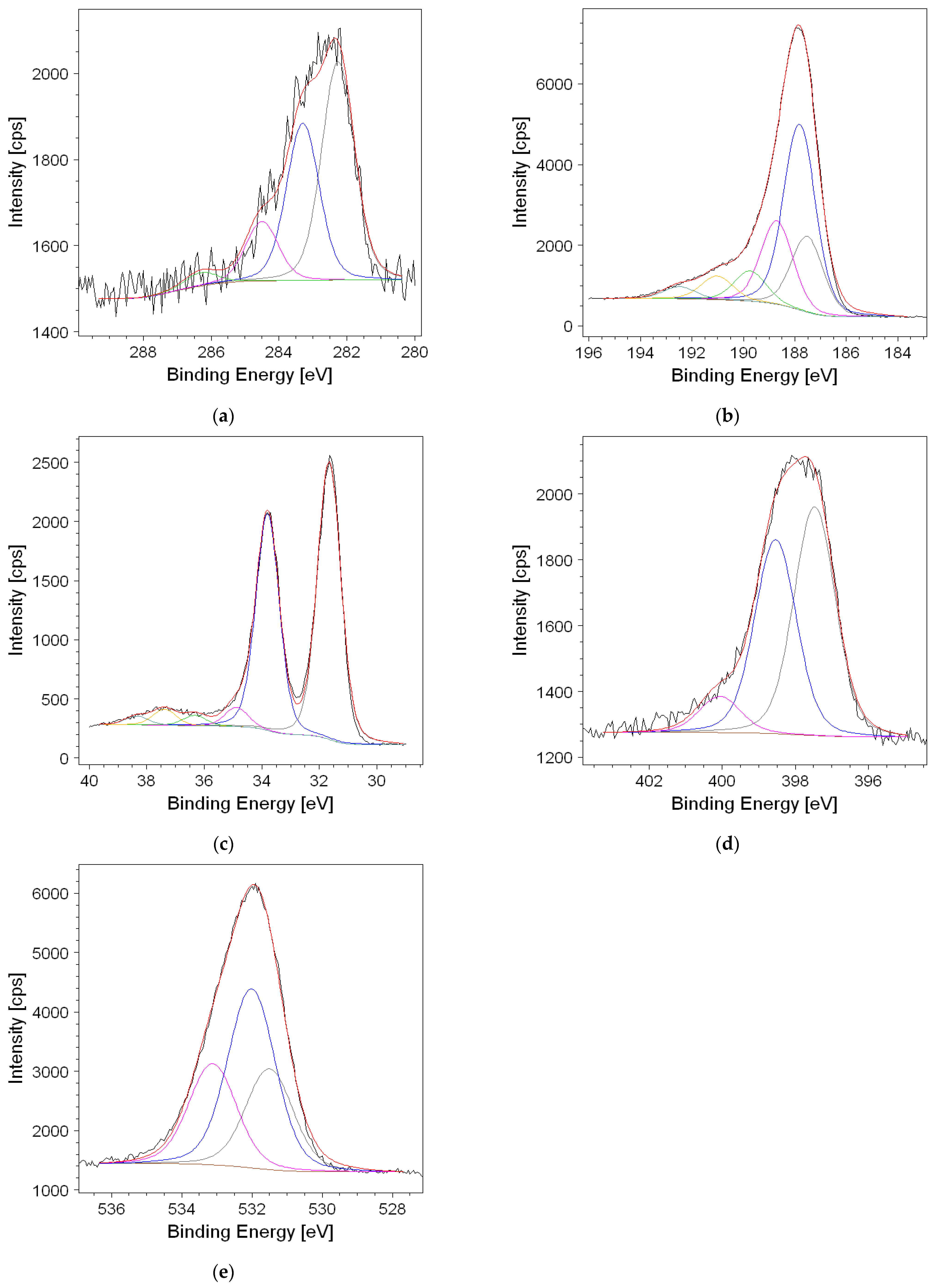
The analyses indicate that, in order to obtain a homogeneous coating with low oxygen content, low roughness and a density as close as possible to that of bulk boron, sputtering should be performed at low pressures, specifically at 0.6 Pa in the present study. For this latter condition, to quantitatively evaluate the B and O contents and investigate possible chemical bonds, including those involving impurities present in the chamber, an XPS measurement was performed. The XPS depth profile shown in Table 1 illustrates the chemical behaviour of each element at the surface (without Ar+ sputtering) and in the near-surface region (after 12.0 min of Ar+ sputtering, approximately 70 nm below the surface) of the sample. The oxygen percentage is consistent with the value determined by EDX. At the surface, N and W were detected (N2 originates from the exposure of the chamber to air, while W contamination results from previous sputtering used to produce the interlayer). However, these elements are associated with high uncertainty due to their low concentrations. C and O show high concentrations at the surface. Most of the detected carbon originates from adventitious contamination caused by air exposure, leading to the adsorption of organic species. The components observed at 284.8 eV and 284.3 eV are attributed to CHx species and graphitic C=C carbon, respectively. The lower binding energy contributions, in the range of 282–283.5 eV, are assigned to carbon–boron and carbon–tungsten (C–W) bonds [40]. The oxygen concentration is also high, largely because boron oxidizes spontaneously in air due to its strong affinity for oxygen. As expected, the concentrations of C and O decrease with depth, while boron evolves structurally into both elemental and impurity-bonded forms. The acquired high-resolution spectra after 12 min of sputtering are peak-fitted into different components (Figure 11).
The peaks at approximately 282 eV and 283 eV (Figure 11a) correspond to carbon atoms bonded to B [12,41,42]. Specifically, they are associated with boron-rich (BxC) and carbon-rich (BCγ) boron carbide, respectively [42,43,44,45,46]. For completeness, although W is always present at concentrations below 1%, WCx bonds may also form in the low-energy region. The peak at around 284.8 eV is mainly attributed to C–C/C–H bonds [47,48,49]. The high-energy component in the 286–287 eV region can be attributed to the presence of carbon in various oxygen-containing groups [19,49,50], some of which correspond to components in the O1s spectrum (Figure 11e) associated with oxygen–carbon bonds. The O1s spectrum can be fitted with components at 531.5 eV, 532.5 eV, and 533.6 eV, assigned to O–C, O=C [50], and O–B bonds [50,51], respectively. It should be noted, however, that a peak in the 531.3–531.7 eV range may also be attributed to oxygen bonded to W [52,53]. The B1s spectrum (Figure 11b) was fitted with six components. The component at 187.5 eV corresponds to the B–B bond [21], in good agreement with the reported value for bulk boron [39,54]. Consistent with the C 1s spectrum, the B 1s signal also contains B–C bonds associated with boron-rich (BxC) and carbon-rich (BCγ) boron carbides at 188 eV and 189 eV, respectively [45,50,55,56]. The peak at around 190 eV can be attributed to boron nitride bonds [57,58]. The feature at approximately 191.7 eV may be assigned to boron oxides, in which an oxygen atom is coordinated with several boron atoms (Bx–O) [39,59,60], and/or to boron oxycarbides [55]. The highest-energy component of the B 1s spectrum, at around 193 eV, together with the corresponding O1s feature at 533.6 eV in Figure 11e, is clearly characteristic of B2O3 [50,54,61]. Tungsten (Figure 11c) appears as a mixture of oxides and carbide. The spin–orbit 4f 7/2 component at a binding energy (BE) of ~31.7 eV is assigned to WCx, while oxidized W in a sub-stoichiometric form is found at around ~35.2 eV [62,63,64,65] and as stoichiometric WO3 at ~36.2 eV [54,63,66]. Nitrogen present as an impurity also forms chemical bonds within the coating. The N1s high-resolution spectrum was decomposed into three components with binding energies of 397.9 eV [67,68], 399.5 eV [69], and 402.0 eV [67], corresponding to nitride, C–N bonds, and NH2 groups, respectively (Figure 11d).

4. Conclusions

Boron (B) coatings with a thickness of approximately 100 nm were deposited on Si substrates by RF magnetron sputtering as a function of sputtering pressure (0.6–5 Pa) at a fixed RF power of 80 W. In order to gain an understanding of the plasma properties in the sputtering system, a Langmuir probe was used to measure the electron temperature (Te) and electron density (ne). These parameters did not show a significant dependence over the pressure range considered. Te remained in the range of 3.7–4.0 eV, while ne was in the range of 1.0–1.1 × 10¹⁶ m−3. Regarding the coatings, the results showed that density, film morphology, and oxygen content are strongly dependent on the sputtering pressure. The lowest process pressure resulted in a smooth B coating with minimal oxygen uptake and higher mass density. In addition, a high reactivity of boron with impurities present in the process chamber was observed, particularly with oxygen (EDX analyses), as evidenced by the formation of boron oxides detected by XPS analyses. Deposition at the lowest sputtering pressure enabled the production of coatings with the lowest oxygen content (~11%), lower roughness, higher density, and a deposition rate of approximately 30 nm/h. Overall, the results show that the influence of sputtering pressure on plasma parameters and coating properties has been successfully assessed, providing new insights into the pressure-dependent trends in boron coating density, surface morphology, and oxygen incorporation, for which no experimental studies under conditions comparable to ours have been reported in the literature.

Author Contributions

Conceptualization, E.V., M.P. and M.S.; investigation, E.V., M.P., M.S., D.R. and G.S.; data curation, E.V., M.P., M.S., D.R. and G.S.; writing—original draft preparation, E.V. and M.P.; writing—review and editing, E.V., M.P., M.S., D.R. and G.S. All authors have read and agreed to the published version of the manuscript.

Funding

This research received no external funding.

Institutional Review Board Statement

Not applicable.

Informed Consent Statement

Not applicable.

Data Availability Statement

The original contributions presented in this study are included in the article material. Further inquiries can be directed to the corresponding author.

Conflicts of Interest

The authors declare no conflicts of interest.

References

  1. Bernard, R.; Pastre, A.; Griboval, A.; Andrieux, V.; Técher, K.; Laffont, G.; Rached, L.L. High-temperature resistant boron nitride-based coatings for specialty silica optical fibers. Opt. Laser Technol. 2025, 181, 111855. [Google Scholar] [CrossRef] [Scilit]
  2. Kaya, O.; Gabatel, L.; Bellani, S.; Barberis, F.; Bonaccorso, F.; Cole, I.; Roche, S. 2D hexagonal boron nitride-based anticorrosion coatings. J. Phys. Mater. 2025, 8, 042002. [Google Scholar] [CrossRef] [Scilit]
  3. Avcıoğlu, S.; Buldu, M.; Kaya, F.; Üstündağ, C.B.; Kam, E.; Menceloğlu, Y.Z.; Kaptan, H.Y.; Kaya, C. Processing and properties of boron carbide (B4C) reinforced LDPE composites for radiation shielding. Ceram. Int. 2020, 46, 343–352. [Google Scholar] [CrossRef] [Scilit]
  4. Wang, Z.; Morris, C. Multi-layer boron thin-film detectors for neutrons. Nucl. Instrum. Methods Phys. Res. A Accel. Spectrometers Detect. Assoc. Equip. 2011, 652, 323–325. [Google Scholar] [CrossRef] [Scilit]
  5. Shao, Q.; Voss, L.F.; Conway, A.M.; Nikolic, R.J.; Dar, M.A.; Cheung, C.L. High aspect ratio composite structures with 48.5% thermal neutron detection efficiency. Appl. Phys. Lett. 2013, 102, 063505. [Google Scholar] [CrossRef] [Scilit]
  6. Oganov, A.R.; Solozhenko, V.L. Boron: A hunt for superhard polymorphs. J. Superhard Mater. 2009, 31, 285–291. [Google Scholar] [CrossRef] [Scilit]
  7. Mannix, A.J.; Zhou, X.; Kiraly, B.; Wood, J.D.; Alducin, D.; Myers, B.D.; Liu, X.; Fisher, B.L.; Santiago, U.; Guest, J.R.; et al. Synthesis of borophenes: Anisotropic, two-dimensional boron polymorphs. Science 2015, 350, 1513–1516. [Google Scholar] [CrossRef] [Scilit] [PubMed]
  8. Sachdev, H. Disclosing boron’s thinnest side. Science 2015, 350, 1468–1469. [Google Scholar] [CrossRef] [Scilit]
  9. Zhao, F.; Zhao, P.; Zhang, X.; Wu, T.; Wang, Q. Transfer-free synthesis of large-area 2D boron films on non-wetting liquid gallium substrate. Phys. B Condens. Matter 2023, 669, 415289. [Google Scholar] [CrossRef] [Scilit]
  10. Lamborn, D.R.; Snyder, D.W.; Xi, X.X.; Redwing, J.M. Modeling studies of the chemical vapor deposition of boron films from B2H6. J. Cryst. Growth 2007, 299, 358–364. [Google Scholar] [CrossRef] [Scilit]
  11. Rehana, I.; Muhammad, D.; Ahmed, S.; Akhter, J.I. Preparation and Characterization of Boron Thin Film on Iron Substrate. J. Mater. Sci. Technol. 2007, 23, 481–486. [Google Scholar]
  12. Tamer, A.; Ekem, N.; Pat, S.; Issever, U.G.; Balbag, M.Z.; Cenik, M.I.; Vladoiu, R.; Musa, G. Boron thin film deposition by using Thermionic Vacuum Arc (TVA) technology. Mater. Lett. 2007, 61, 23. [Google Scholar] [CrossRef] [Scilit]
  13. Yushkov, Y.; Oks, E.; Kazakov, A.; Tyunkov, A.; Zolotukhin, D. Electron-Beam Synthesis and Modification and Properties of Boron Coatings on Alloy Surfaces. Ceramics 2022, 5, 706–720. [Google Scholar] [CrossRef] [Scilit]
  14. Dellasega, D.; Russo, V.; Pezzoli, A.; Conti, C.; Lecis, N.; Besozzi, E.; Beghi, M.; Bottani, C.E.; Passoni, M. Boron films produced by high energy Pulsed Laser Deposition. Mater. Des. 2017, 134, 35–43. [Google Scholar] [CrossRef] [Scilit]
  15. Danışman, Ş.; Odabaş, D.; Teber, M. The Effect of TiN, TiAlN, TiCN Thin Films Obtained by Reactive Magnetron Sputtering Method on the Wear Behavior of Ti6Al4V Alloy: A Comparative Study. Coatings 2022, 12, 1238. [Google Scholar] [CrossRef] [Scilit]
  16. Stankus, V.; Vasiliauskas, A.; Guobienė, A.; Andrulevičius, M.; Meškinis, Š. Synthesis and Characterization of Boron Nitride Thin Films Deposited by High-Power Impulse Reactive Magnetron Sputtering. Molecules 2024, 29, 5247. [Google Scholar] [CrossRef] [Scilit] [PubMed]
  17. Pan, Z.; Yang, Y.; Huang, J.; Ren, B.; Yu, H.; Xu, R.; Ji, H.; Wang, L.; Wang, L. Study on the preparation of boron-rich film by magnetron sputtering in oxygen atmosphere. Appl. Surf. Sci. 2016, 388, 392–395. [Google Scholar] [CrossRef] [Scilit]
  18. Vizir, A.V.; Nikolaev, A.G.; Oks, E.M.; Frolova, V.P.; Cherkasov, A.A.; Shandrikov, M.V.; Yushkov, G.Y. Physical Features of the Functioning of a Planar Magnetron Sputter with a Thermally Insulated, Discharge-Heated Target for Boron Coating Deposition. Russ. Phys. J. 2022, 64, 2177–2184. [Google Scholar] [CrossRef] [Scilit]
  19. Mijatovic, D.; Brinkman, A.; Hilgenkamp, H.; Rogalla, H.; Rijnders, G.; Blank, D. Pulsed laser deposition of MgB2 and B thin films. Appl. Phys. A-Mater. 2004, 79, 1243–1246. [Google Scholar] [CrossRef] [Scilit]
  20. Chen, F.F.; Chang, J.P. Langmuir Probes. In Lecture Notes on Principles of Plasma Processing; Springer: Boston, MA, USA, 2003. [Google Scholar]
  21. Vassallo, E.; Saleh, M.; Pedroni, M.; Cremona, A.; Ripamonti, D. Characterization of Tungsten Sputtering Processes in a Capacitively Coupled Argon Plasma. Plasma 2025, 8, 8. [Google Scholar] [CrossRef] [Scilit]
  22. Vassallo, E.; Pedroni, M.; Aloisio, M.; Minelli, D.; Nardone, A.; Chen, H.; Pietralunga, S.M.; Stinchelli, A.; Di Fonzo, F. Study of process parameters and characteristics properties of W coatings deposited by rf plasma sputtering. J. Vac. Sci. Technol. B 2023, 41, 032802. [Google Scholar] [CrossRef] [Scilit]
  23. Chen, F.F. Langmuir probe diagnostics. In Proceedings of the 2003 IEEE—International Conference on Plasma Science (ICOPS), Jeju, Republic of Korea, 2–5 June 2003. [Google Scholar]
  24. Sudit, I.D.; Woods, R.C. A workstation based Langmuir probe system for low-pressure dc plasmas. Rev. Sci. Instrum. 1993, 64, 2440. [Google Scholar] [CrossRef] [Scilit]
  25. Druyvesteyn, M.J. Der Niedervoltbogen. Eur. Phys. J. A 1930, 64, 781–798. [Google Scholar] [CrossRef] [Scilit]
  26. Lieberman, M.A.; Lichtenberg, A.J. Principles of Plasma Discharges and Materials Processing, 2nd ed.; Wiley: New York, NY, USA, 1994. [Google Scholar]
  27. Speranza, G. Data Driven Guide to the Analysis of X-Ray Photoelectron Spectra Using RxpsG, 1st ed.; CRC Press: Boca Raton, FL, USA, 2023. [Google Scholar]
  28. Ivanov, I.; Statev, S.; Orlinov, V.; Shkevov, R. Electron energy distribution function in a dc magnetron sputtering discharge. Vacuum 1992, 43, 837. [Google Scholar] [CrossRef] [Scilit]
  29. Vass, M.; Wilczek, S.; Lafleur, T.; Brinkmann, R.P.; Donkó, Z.; Schulze, J. Electron power absorption in low pressure capacitively coupled electronegative oxygen radio frequency plasmas. J. Plasma Sources Sci. Technol. 2020, 29, 025019. [Google Scholar] [CrossRef] [Scilit]
  30. Lopez, J.L.; Brunger, M.; Kersten, H. Electron-driven processes from single collisions to high-pressure plasmas. Eur. Phys. J. D 2023, 77, 154. [Google Scholar] [CrossRef] [Scilit]
  31. Kusano, E.; Fukushima, K.; Saitoh, T.; Saiki, S.; Kikuchi, N.; Nanto, H.; Kinbara, A. Effects of Ar pressure on ion flux energy distribution and ion fraction in r.f.-plasma-assisted magnetron sputtering. Surf. Coat. Technol. 1999, 120–121, 189–193. [Google Scholar] [CrossRef] [Scilit]
  32. Feng, B.; Zhang, J.; Zhong, Q.; Li, W.; Li, S.; Li, H.; Cheng, P.; Meng, S.; Chen, L.; Wu, K. Experimental realization of two-dimensional boron sheets. Nat. Chem. 2016, 86, 563–568. [Google Scholar] [CrossRef] [Scilit] [PubMed]
  33. Cao, L.; Zhang, Z.; Wang, W. Magnetron sputtering synthesis of large area well-ordered boron nanowire arrays. Sci. China Ser. G Phys. Mech. Astron. 2004, 47, 403–415. [Google Scholar] [CrossRef] [Scilit]
  34. Bayu Aji, L.B.; Baker, A.A.; Bae, J.H.; Hiszpanski, A.M.; Stavrou, E.; McCall, S.K.; Kucheyev, S.O. Degradation of ultra-thin boron films in air. Appl. Surf. Sci. 2018, 448, 498–501. [Google Scholar] [CrossRef] [Scilit]
  35. Yushkov, G.Y.; Gridilev, V.D.; Nikolaev, A.G. Features of Magnetron Deposition by Sputtering Boron Target in Reactive Gases Medium. J. Surf. Investig. 2024, 18, S84–S90. [Google Scholar] [CrossRef] [Scilit]
  36. Hino, T.; Mochizuki, T.; Hirohata, Y.; Tsuzuki, K.; Inoue, N.; Sagara, A.; Noda, N.; Motojima, O.; Mori, K.; Sogabe, T.; et al. Oxygen gettering properties of boron film produced by diborane dc glow discharge. J. Nucl. Mater. 1997, 248, 38–41. [Google Scholar] [CrossRef] [Scilit]
  37. Yang, Y.C.; Chang, C.T.; Hsiao, Y.C.; Lee, J.W.; Lou, B.S. Influence of high power impulse magnetron sputtering pulse parameters on the properties of aluminum nitride coatings. Surf. Coat. Technol. 2014, 259, 219–231. [Google Scholar] [CrossRef] [Scilit]
  38. Berman, A. Water vapor in vacuum systems. Vacuum 1996, 47, 327–332. [Google Scholar] [CrossRef] [Scilit]
  39. Ennaceur, M.M.; Terreault, B. XPS study of the process of oxygen gettering by thin films of PACVD boron. J. Nucl. Mater. 2000, 280, 33–38. [Google Scholar] [CrossRef] [Scilit]
  40. NIST. NIST X-Ray Photoelectron Spectroscopy Database—Version 5.0. 2023. Available online: https://srdata.nist.gov/xps/ (accessed on 3 November 2025).
  41. Künzli, H.; Gantenbein, P.; Steiner, R.; Oelhafen, P. Deposition and Characterization of Thin Boron-Carbide Coatings. Fresenius’ J. Anal. Chem. 1993, 346, 41–44. [Google Scholar] [CrossRef] [Scilit]
  42. Yang, Q.; Wang, C.B.; Zhang, S.; Zhang, D.M.; Shen, Q.; Zhang, L.M. Effect of Nitrogen Pressure on Structure and Optical Properties of Pulsed Laser Deposited BCN Thin Films. Surf. Coat. Technol. 2010, 204, 1863–1867. [Google Scholar] [CrossRef] [Scilit]
  43. Ronning, C.; Schwen, D.; Eyhusen, S.; Vetter, U.; Hofsäss, H. Ion synthesis of boron carbide thin films. Surf. Coat. Technol. 2002, 382–387, 158–159. [Google Scholar] [CrossRef] [Scilit]
  44. Wada, Y.; Yap, Y.K.; Yoshimura, M.; Mori, Y.; Sasaki, T. The control of B N and B C bonds in BCN films synthesized using pulsed laser deposition. Diam. Relat. Mater. 2000, 9, 620–624. [Google Scholar] [CrossRef] [Scilit]
  45. Mannan, A.; Nagano, M.; Kida, T.; Hirao, N.; Baba, Y. Characterization of BCN films synthesized by radiofrequency plasma enhanced chemical vapor deposition. J. Phys. Chem. Solids 2009, 70, 20–25. [Google Scholar] [CrossRef] [Scilit]
  46. Qian, J.C.; Zhou, Z.F.; Yan, C.; Li, D.J.; Li, K.Y.; Descartes, S.; Chromik, R.; Zhang, W.J.; Bello, I.; Martinu, L.; et al. Tailoring the mechanical and tribological properties of sputtered boron carbide films via the B1-xCx composition. Surf. Coat. Technol. 2015, 267, 2–7. [Google Scholar] [CrossRef] [Scilit]
  47. Norimatsu, W.; Matsuda, K.; Terasawa, T.-O.; Takata, N.; Masumori, A.; Ito, K.; Oda, K.; Ito, T.; Endo, A.; Funahashi, R. Controlled growth of boron-doped epitaxial graphene by thermal decomposition of a B4C thin film. Nanotechnology 2020, 31, 145711. [Google Scholar] [CrossRef] [Scilit]
  48. Behera, S.; Wilks, J.; Dowben, P.A.; Driver, M.S.; Caruso, A.N.; Kelber, J.A. Photo-induced site-specific nitridation of plasma deposited B10C2Hx films: A new pathway toward post-deposition doping of semiconducting boron carbides. Surf. Sci. 2010, 604, 21–22. [Google Scholar] [CrossRef] [Scilit]
  49. Vickerman, J.C. (Ed.) Surface Analysis—The Principle Techniques; John Wiley & Sons: Chichester, UK, 1997. [Google Scholar]
  50. Sulyaeva, V.; Khomyakov, M.; Kosinova, M. Room-Temperature Formation of Hard BCx Films by Low Power Magnetron Sputtering. Appl. Sci. 2021, 11, 9896. [Google Scholar] [CrossRef] [Scilit]
  51. Reisse, G.; Weissmantel, S.; Keiper, B.; Weber, A. Properties of pulsed laser deposited boron nitride films. Appl. Surf. Sci. 1997, 108, 9–15. [Google Scholar] [CrossRef] [Scilit]
  52. Chen, H.; Chiasera, A.; Varas, S.; Sayginer, O.; Armellini, C.; Speranza, G.; Suriano, R.; Ferrari, M.; Pietralunga, S.M. Tungsten oxide films by radio-frequency magnetron sputtering for near-infrared photonics. Opt. Mater. X 2021, 12, 100093. [Google Scholar] [CrossRef] [Scilit]
  53. Riech, I.; Acosta, M.; Peña, J.L.; Bartolo-Pérez, P. Effects of working pressure on physical properties of tungsten-oxide thin films sputtered from oxide target. J. Vac. Sci. Technol. A 2010, 28, 329–333. [Google Scholar] [CrossRef] [Scilit]
  54. Moulder, J.; Stickle, W.; Sobel, P.; Bomben, E. Handbook of X-Ray Photoelectron Spectroscopy; Chastain, J., King, R.C., Eds.; Physical Electronics: Eden Prairie, MN, USA, 1995. [Google Scholar]
  55. Hu, T.; Steihl, L.; Rafaniello, W.; Fawcett, T.; Hawn, D.D.; Mashall, J.G.; Rozeveld, S.G.; Putzig, C.L.; Blackson, J.H.; Cermignani, W.; et al. Structures and properties of disordered boron carbide coatings generated by magnetron sputtering. Thin Solid Film. 1998, 332, 80–86. [Google Scholar] [CrossRef] [Scilit]
  56. Bao, R.; Chrisey, D.B. Chemical states of carbon in amorphous boron carbide thin films deposited by radio frequency magnetron sputtering. Thin Solid Film. 2010, 519, 164–168. [Google Scholar] [CrossRef] [Scilit]
  57. Crist, B.V. Rare earth oxides, hydroxides, carbonates, nitrides, sulfides, and miscellaneous materials. In Handbooks of Monochromatic XPS Spectra; John Wiley & Sons Inc.: Chichester, UK, 2000; Volume 5. [Google Scholar]
  58. Jiang, L.; Fitzgerald, A.G.; Rose, M.J.; Lousa, A.; Gimeno, S. Formation of cubic boron nitride films by r.f. magnetron sputtering. Surf. Interface Anal. 2002, 34, 732–734. [Google Scholar] [CrossRef] [Scilit]
  59. Belyansky, M.; Trenary, M.; Ellison, C. Boron Chemical Shifts in B6O. Surf. Sci. Spectra 1994, 3, 147–150. [Google Scholar] [CrossRef] [Scilit]
  60. Wang, Y.; Trenary, M. Characterization with XPS of a thin film of B2O2 deposited on a Ag substrate. Surf. Sci. Spectra 1992, 1, 183–187. [Google Scholar] [CrossRef] [Scilit]
  61. Wang, Y.; Trenary, M. Surface chemistry of boron oxidation. 2. The reactions of boron oxides B2O2 and B2O3 with boron films grown on tantalum(110). Chem. Mater. 1993, 5, 199–205. [Google Scholar] [CrossRef] [Scilit]
  62. Marin, A.; Saefan, A.; Unterberg, E.; Parish, C.M.; Bernard, E.; Diez, M.; Tsitrone, E.; Wang, X. XPS post-mortem analysis of plasma-facing units extracted from WEST after the C3 (2018) and C4 (2019) campaigns. J. Nucl. Mater. 2025, 604, 155525. [Google Scholar] [CrossRef] [Scilit]
  63. Barreca, D.; Carta, G.; Gasparotto, A.; Rossetto, G.; Tondello, E.; Zanella, P. A study of nanophase tungsten oxides thin films by XPS. Surf. Sci. Spectra 2001, 8, 258–267. [Google Scholar] [CrossRef] [Scilit]
  64. Bouvard, O.; Krammer, A.; Schüler, A. In situ core-level and valence-band photoelectron spectroscopy of reactively sputtered tungsten oxide films. Surf. Interface Anal. 2016, 48, 660–663. [Google Scholar] [CrossRef] [Scilit]
  65. Romanyuk, A.; Oelhafen, P. Evidence of different oxygen states during thermal coloration of tungsten oxide. Sol. Energy Mater. Sol. Cells 2006, 90, 1945. [Google Scholar] [CrossRef] [Scilit]
  66. Colton, R.J.; Wayne, J. Rabalais, Electronic structure to tungsten and some of its borides, carbides, nitrides, and oxides by x-ray electron spectroscopy. Inorg. Chem. 1976, 15, 236–238. [Google Scholar] [CrossRef] [Scilit]
  67. Gouin, X.; Grange, P.; Bois, L.; L’Haridon, P.; Laurent, Y. Characterization of the nitridation process of boric acid. J. Alloys. Compd. 1995, 224, 22–28. [Google Scholar] [CrossRef] [Scilit]
  68. Jean-Remy, P.M.; Cabral, M.J.; Davis, R.F. Flow-modulated deposition of sp2-boron nitride using diborane and ammonia on chemomechanically polished (0001) 4H-SiC substrates. J. Vac. Sci. Technol. A 2022, 40, 023409. [Google Scholar] [CrossRef] [Scilit]
  69. Gammon, W.J.; Kraft, O.; Reilly, A.C.; Holloway, B.C. Experimental comparison of N(1s) X-ray photoelectron spectroscopy binding energies of hard and elastic amorphous carbon nitride films with reference organic compounds. Carbon 2003, 41, 1917–1923. [Google Scholar] [CrossRef] [Scilit]
Figure 1. I–V characteristics of the probe for the plasma discharge with a boron target and an RF power of 80 W at different sputtering pressures.
Surfaces 09 00031 g001
Figure 2. Electron energy probability functions (EEDs) as a function of pressure at 80 W of input power.
Surfaces 09 00031 g002
Figure 3. Te as a function of the sputtering pressure at a fixed RF power of 80 W.
Surfaces 09 00031 g003
Figure 4. ne as a function of the sputtering pressure at a fixed RF power of 80 W.
Surfaces 09 00031 g004
Figure 5. Top-view (a) and cross-sectional (b) SEM images of the deposited B coatings deposited at 5 Pa.
Surfaces 09 00031 g005
Figure 6. Boron DR and coating density as a function of the sputtering pressure at a fixed RF power of 80 W.
Surfaces 09 00031 g006
Figure 7. Estimated value of the mean free path of the B atoms at various Ar pressures.
Surfaces 09 00031 g007
Figure 8. O (at.%) of W coatings grown as a function of pressure (at fixed RF power of 80 W).
Surfaces 09 00031 g008
Figure 9. SEM cross-sectional images of the boron coatings deposited as a function of pressure: (a) 0.6 Pa, (b) 1.2 Pa and (c) 2.4 Pa.
Surfaces 09 00031 g009
Figure 10. AFM images of boron coatings deposited as a function of pressure: (a) 0.6 Pa, (b) 1.2 Pa and (c) 2.4 Pa.
Surfaces 09 00031 g010
Figure 11. XPS peak-fitted spectra of B coating at 0.6 Pa after 12.0 min of Ar+_ion sputtering: (a) C1s, (b) B1s, (c) W4f, (d) N1s, and (e) O1s.
Surfaces 09 00031 g011
Table 1. Relative elemental concentrations (at.%) and calculated information depth (nm) for the sample deposited at 0.6 Pa.
Ar+ Sputtering TimeB1sO1sC1sN1sW4fDepth (nm)
0.0 min59.820.918.20.80.30
12.0 min 81.011.43.33.31.070
Disclaimer/Publisher’s Note: The statements, opinions and data contained in all publications are solely those of the individual author(s) and contributor(s) and not of MDPI and/or the editor(s). MDPI and/or the editor(s) disclaim responsibility for any injury to people or property resulting from any ideas, methods, instructions or products referred to in the content.