Article

Global–Local Cooperative Optimization in Photonic Inverse Design Algorithms

1
School of Electrical and Information Engineering, Tianjin University, Tianjin 300072, China
2
Tianjin Key Laboratory of Brain-Inspired Intelligence Technology, Tianjin 300072, China
*
Author to whom correspondence should be addressed.
Photonics 2025, 12(7), 725; https://doi.org/10.3390/photonics12070725
Submission received: 12 June 2025 / Revised: 11 July 2025 / Accepted: 15 July 2025 / Published: 17 July 2025
(This article belongs to the Special Issue Recent Progress in Integrated Photonics)

Abstract

We developed the Global–Local Integrated Topology inverse design algorithm (denoted as the GLINT algorithm), which employs a trajectory-based optimization strategy with waveguide–substrate material-flipping structural modifications, enabling the direct optimization of discrete waveguide–substrate binary structures. Compared to the conventional Direct Binary Search (DBS), the GLINT algorithm not only significantly enhances computational efficiency through its global search–local refinement framework but also achieves a superior 20 nm × 20 nm optimization resolution while maintaining its optimization speed—substantially advancing the design capability. Utilizing this algorithm, we designed and experimentally demonstrated a 3.5 µm × 3.5 µm dual-port wavelength division multiplexer (WDM), achieving a minimum crosstalk of −11.3 dB and a 2 µm × 2 µm 90-degree bending waveguide exhibiting a 0.31–0.52 dB insertion loss over the 1528–1600 nm wavelength range, both fabricated on silicon-on-insulator (SOI) wafers. Additionally, a 4.5 µm × 4.5 µm three-port WDM structure was also designed and simulated, demonstrating crosstalk as low as −36.5 dB.

1. Introduction

Integrated photonic devices are crucial for advancing modern optical technologies, facilitating breakthroughs in high-speed communication [1], quantum information processing [2], and biosensing [3]. Traditional design strategies often focus on optimizing a limited set of geometric parameters, such as waveguide widths or cavity radii, which are typically confined to predefined regular shapes. Although this approach is straightforward, it significantly restricts design freedom by confining solutions to low-dimensional design spaces that struggle to meet the increasing demand for compact, high-performance devices capable of exploiting complex light–matter interactions. To address these limitations, inverse design methodologies have emerged as a transformative paradigm [4], utilizing computational optimization to explore high-dimensional design spaces and unlock photonic devices with unprecedented functionality, enabling innovations from the three-channel wavelength demultiplexer [5] to meta-dispersion microresonators [6] and non-reciprocal pulse routers [7]. These advancements highlight the paradigm’s capability to surpass traditional design constraints, establishing it as an essential tool for next-generation integrated photonics [8,9,10,11,12,13].
Despite these achievements, current mainstream adjoint-based inverse design approaches utilizing density topology optimization (DTO) [14,15,16] face a critical challenge that substantially constrains the optimization efficiency. The inherent assumption of a spatially continuous refractive index distribution within this framework fundamentally conflicts with practical fabrication requirements. The mandatory binarization process for discretizing continuous refractive indices may completely negate the carefully optimized optical characteristics, thereby necessitating optimization reinitialization, which significantly compromises the design efficiency. While level-set optimization (LST) [17,18] algorithms are commonly combined with DTO [5,18,19] to mitigate this issue through the direct boundary optimization of binary structures, their standalone application suffers from critical limitations. Specifically, LST methods can only modify existing boundaries or internal cavities but cannot spontaneously generate new void structures within solid regions, thus requiring complementary optimization strategies for a practical implementation.
Alternative approaches such as direct binary search (DBS) [20,21,22,23,24,25,26] algorithms and rotatable DBS [27] variants circumvent the continuous refractive index assumption by discretizing the design space into rectangular or circular pixels. However, such pixel-based methods suffer from two critical drawbacks. First, these methods sacrifice substantial design freedom compared to DTO approaches, with typical pixel dimensions (~100 nm × 100 nm) being excessively large, severely constraining their optimization flexibility. Second, prohibitive computational demands stemming from exhaustive pixel-by-pixel searching in DBS algorithms render these methods impractical for large-scale or functionally complex photonic devices.
In this work, we introduce a Global–Local Integrated Topology inverse design algorithm, denoted throughout this work as the GLINT algorithm or the GLINT inverse design algorithm, that addresses these challenges through an iterative optimization framework. Our approach strategically combines a global search for a rapid performance improvement and local refinement for precision tuning. The global search phase rapidly identifies promising design regions where structural modifications yield significant performance gains, while the local refinement phase progressively refines geometries within these regions through meticulous parameter adjustments. When the local refinement stagnates, the algorithm automatically reactivates the global search to locate new optimization zones, cycling between these modes until target specifications are achieved. Crucially, our method not only eliminates the continuous refractive index assumption inherent in DTO algorithms but also, compared to the DBS algorithm, significantly enhances the design freedom and computational efficiency.
To validate our approach, we experimentally demonstrate its efficacy through the realization of two compact devices: a two-port wavelength division multiplexer (WDM) and a 90-degree bending waveguide. Additionally, we numerically design a three-port WDM, showcasing the algorithm’s capability to handle increasingly complex design challenges. Remarkably, the 90-degree bending waveguide occupies a footprint of just 2 µm × 2 µm, while the two-port and three-port WDMs measure 12.25 µm2 and 20.25 µm2, respectively. These results highlight the algorithm’s ability to achieve ultra-compact device geometries, significantly reducing spatial requirements for chip layouts and paving the way for large-scale, densely integrated photonic circuits.

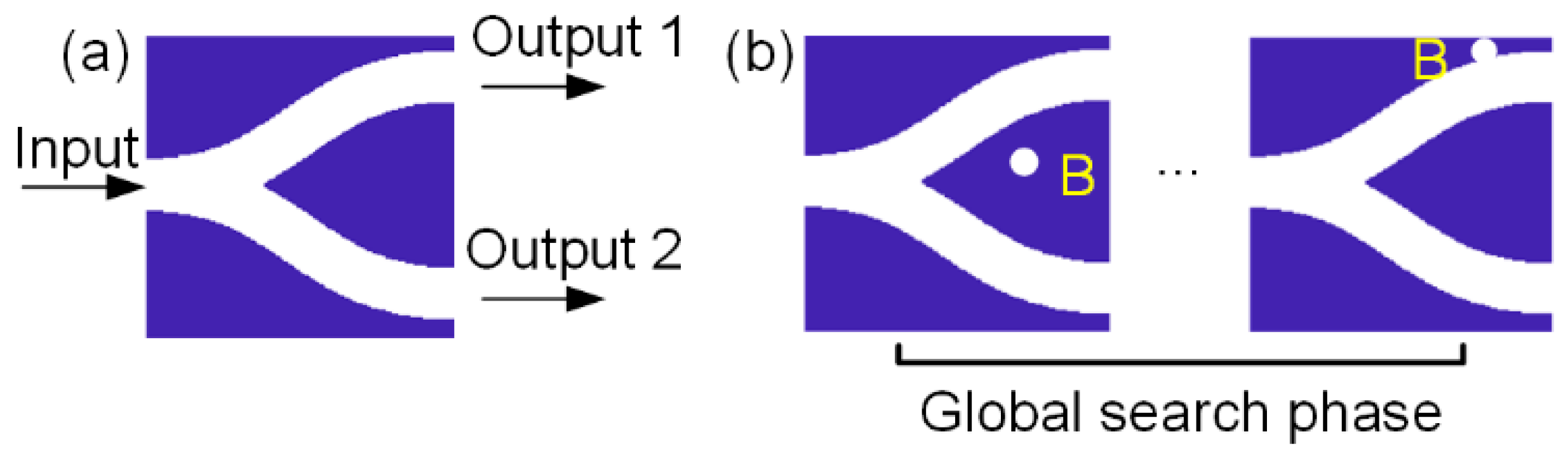
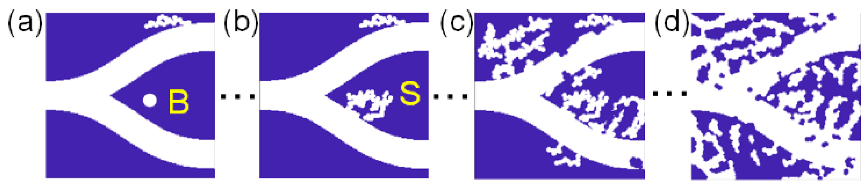
2. The Principle of the GLINT Inverse Design Algorithm

The underlying principle of the GLINT inverse design algorithm can be illustrated through a WDM design example. In this example, all simulations employed a 3D finite-difference time-domain (3D-FDTD) methodology with a spatial resolution of 20 nm × 20 nm, uniform perfectly matched layer (PML) boundary conditions, and transverse-electric (TE) polarized excitation sources. The optimization domain is defined with dimensions of 3.5 µm × 3.5 µm × 220 nm. The substrate material is silicon dioxide (represented in white), and the waveguide material is silicon (represented in blue). To facilitate global search and local refinement operations, the optimization domain is subdivided into a uniform grid with a cell size of 20 nm × 20 nm. Notably, the grid size (20 nm × 20 nm in this work) defines the minimum feature size of the optimized structures. While this parameter is not fixed and can be scaled according to fabrication capabilities, all designs in this study adopt 20 nm × 20 nm features to rigorously validate the GLINT algorithm’s performance under near-lithographic-resolution constraints. Figure 1a illustrates the initial structure, where the silicon (white) and silica (blue) regions are clearly defined. Two input signals at λ1 = 1607.5 nm and λ2 = 1528.8 nm enter from the left port, with the design objective of routing λ1 to output port 1 and λ2 to port 2. Notably, GLINT allows the free selection of initial structures—including fully waveguide- or substrate-filled configurations. However, better initial structures could reduce the optimization time. To assess the device’s performance, the fundamental principle governing the Figure of Merit (FOM) formulation dictates that as the performance of the optimized structure asymptotically approaches the target performance, the FOM converges toward 0; conversely, the deviation from the target performance drives the FOM toward 1. For this work, we define the FOM as
F O M = 1 P 1 ( λ 1 ) P i n ( λ 1 ) P 2 ( λ 2 ) P i n ( λ 2 )
where Pin(λi) is the input power at wavelength λi, and Pi(λi) is the output power at λi from port i (i = 1,2). The optimization target aims to minimize this FOM (ideally to zero) through iterative structural modifications. After each iteration, the updated FOM value is denoted as FOM0.
As shown in Figure 1b, the algorithm initiates the global search by randomly selecting the circular region B within the design area (in this case, the radius of region B is 80 nm). The temporary material inversion (silicon ↔ silica) within B generates a trial structure, followed by the trial FOM calculation (FOMt). After restoring the original configuration, this process repeats with new random regions until it identifies a candidate satisfying
F O M 0 F O M t F O M 0 > G t h
where Gth is the global searching threshold. The processes illustrated in Figure 1b are termed the global search phase, and the qualified region B is referred to as the global optimization area.
As demonstrated in Figure 2a, once a circular region B meets the specified condition (2), it is condensed to a smaller concentric circular region S (in this case, the radius of region S is 40 nm), referred to as the local optimization area. Within this region, the materials are permanently inverted, and FOM0 is updated to reflect the current FOM value. Thereafter, the algorithm randomly selects a small adjacent region X next to S (Figure 2b), inverts the materials in X, calculates the trial value FOMt, and then restores the materials in X. Repeat the above procedures until the following condition is met:
F O M 0 F O M t F O M 0 > L t h
where Lth is the local refinement threshold. When the region X satisfies the aforementioned condition (3), it is integrated into S (i.e., S = SX) (Figure 2c), subsequent to a permanent inversion of the materials in X and an update of FOM0. The above procedures occurring in the vicinity of S are referred to as the local refinement phase, and the local optimization area S has the potential to expand through successive local searches until no adjacent region X meets the specified condition (Figure 2d). Once this occurs, the local refinement terminates, and a new cycle of the global search initiates (Figure 3a). The algorithm alternates between the global search and local refinement (Figure 3a–c) until FOM0 achieves a value below a predefined performance threshold (FOMs) or the cumulative number of search steps executed during either the global search or local refinement phases exceeds the preset maximum iteration limit (Figure 3d).
It is critical to emphasize that within the GLINT algorithm, the dimensions of regions B and S are user-configurable parameters that can either remain fixed or dynamically adapt during optimization, depending on specific optimization requirements. Let RB and RS denote the radii of regions B and S, respectively. Upon the completion of each local refinement phase and before recommencing the global search procedure, both parameters (RB and RS) can be adaptively adjusted based on the optimization progress. While a reduction in the size of region B inherently increases the global search duration, this strategy becomes essential when larger initial B regions fail to identify domains satisfying the global search threshold Gth. Under such conditions, strategically downsizing region B enables an accelerated convergence toward Gth-compliant regions, thereby significantly enhancing the algorithm’s search efficiency in complex optimization scenarios. Similarly, Gth and Lth serve as adjustable parameters in the GLINT framework, and when tuning RB and RS in the algorithm, Gth and Lth can be simultaneously adjusted. In the presented example, these thresholds were empirically initialized at Gth = 0.01 and Lth = 0.001. The precise adjustment of Gth, Lth, and the dimensions of regions B and S is critical for identifying higher-quality local optima throughout the optimization process. To prevent the algorithm from stagnating due to a premature convergence to suboptimal local optima, we recommend employing larger initial parameters (1 > Gth ≥ 0.01; GthLth ≥ 0.001; RB ≥ 120 nm; RBRS ≥ 60 nm) and progressively scaling them down throughout iterations. This adaptive strategy ensures balanced exploration–exploitation trade-offs, coordinating the rates of the search efficiency and the FOM reduction across the optimization trajectory. Notably, the selection of Gth and Lth retains full flexibility. Practitioners may alternatively initialize smaller optimization thresholds (e.g., Gth = 1 × 10⁻⁵, Lth = 1 × 10⁻⁷) along with reduced B and S dimensions (e.g., RB = 20 nm, RS = 10 nm) to prioritize the rapid acquisition of functionally viable devices, albeit with an increased risk of premature convergence to suboptimal local optima. This configurability empowers users to tailor the optimization workflow to application-specific priorities.
The GLINT inverse design algorithm introduces two fundamental advancements over the conventional DBS algorithm: First, it employs a dual-phase strategy integrating the global search with the local refinement, achieving a minimum feature size comparable to DTO (20 nm × 20 nm). This high-resolution capability enables the full exploitation of the optimization potential within the design space, directly resolving the limited flexibility issue inherent in the pixel-based DBS algorithm. Second, the global–local optimization architecture significantly enhances the computational efficiency through the rapid identification of critical optimization regions during the global phase, thereby addressing the computational inefficiency inherent in conventional DBS algorithms. Collectively, these innovations expand the applicability of the GLINT inverse design to complex photonic devices while simultaneously improving the computational efficiency and design flexibility. In the subsequent section, the practicability of our algorithm will be demonstrated by several examples.

3. Simulation and Experimental Results

3.1. Dual-Port WDM Structure

The complete simulation flow of the 1528.8/1607.5 nm WDM structure’s crosstalk–iteration relationship (Section 2 case study) is presented in Figure 4a. Notably, this case maintains fixed RB and RS dimensions, with Gth and Lth adjusted only when algorithmic stagnation occurs due to undiscoverable regions satisfying conditions (2) and (3)—a deliberate configuration to benchmark the worst-case optimization speed. Utilizing a single i9-10900K CPU, the total optimization required 240 h across 1360 iterations. The slower optimization speed of this WDM structure is primarily attributed to the progressively diminishing probability of discovering region B configurations that satisfy the FOM reduction threshold during later optimization stages, where global search operations demanded excessive computational resources. Although reducing RB/RS would accelerate the search velocity in regions B/S and facilitate the escape from suboptimal local optima, these parameters were intentionally kept fixed in this case to validate the worst-case optimization performance.
Within Figure 4a, intermediate structures at iterations 1110 and 1215 exemplify GLINT’s progressive optimization deceleration. At iteration 1110 (62 h), both ports’ crosstalk reached −11.7 dB. By iteration 1215 (110 h), the crosstalk improved to −13.5 dB (upper port) and −11.7 dB (lower port). The markedly slower progression between iterations 1110 and 1215 indicates approaching optimization bottlenecks near local optima. Despite this, we continued reducing Gth/Lth thresholds to evaluate the performance characteristics of this local optimum. Upon reaching 240 h, the iteration rate degraded to approximately 1 step/3 h without the RB/RS adjustment, confirming the proximity to a local optimum. Final crosstalk values of −14.4 dB (upper port) and −12.5 dB (lower port) represent marginal improvements (<1 dB for both ports) over the 1215-iteration solution despite 130 additional hours. We emphasize that this configuration represents a near-optimal local solution (not global optimum) obtained within 110 h without parameter precise tuning. The precise co-optimization of RB, RS, Gth, and Lth would yield faster searching and superior local optima approaching the global optimum performance.
The schematic of the final optimized structure is shown in Figure 4b. The electric field distributions for input signals at wavelengths of 1607.5 nm and 1528.8 nm are depicted in Figure 4d and Figure 4e, respectively, clearly demonstrating that the energy at different wavelengths is directed to different output ports. The upper port achieves a −14.4 dB crosstalk at 1607.5 nm, while the lower port provides a −12.5 dB crosstalk at 1528.8 nm, as shown in Figure 4f. To enable the systematic performance evaluation of the WDM structure, we define the normalized transmission ratio, denoted as T. More specifically, Ti designates this metric for the i-th output port, expressed as T i = P i / k P k , where i, k ∈ (up, down) and Pi are the output power at port i.
All nanostructures presented herein were fabricated via industry-standard electron beam lithography (EBL) with subsequent inductively coupled plasma (ICP) dry etching and wet chemical stripping, achieving minimum feature widths of 20 nm (±10 nm tolerance). The designed structure was fabricated on an SOI wafer. In the experimental setup, the output from a tunable laser source is directed through a polarization controller and into a lensed fiber, which subsequently couples the light to the face of the test chip. The output is similarly collected using a lensed fiber and measured by a power meter. To enhance the optical coupling efficiency at the chip’s end face, inverse taper structures were introduced. Figure 4c shows an SEM image of the fabricated structure. It can be seen that several fine features present in Figure 4b are missing in Figure 4c. These deviations result in experimental normalized transmission ratio measurements (indicated by the red and blue dashed lines in Figure 4f) that do not closely match those simulation results, leading to an increased crosstalk of −9.7 dB at the upper port and −11.3 dB at the lower port, respectively. Similarly, the insertion loss (black dashed lines in Figure 4f) has also increased compared to the simulation results. These fine structural features originate from interstices between discrete circular refinement zones during the local optimization phase. When present in excessive quantities, such non-manufacturable features (<40 nm) significantly enlarge the discrepancy between simulated and experimental results. In our future work, these fine structural features will be effectively removed through spatial filtering, a heuristic learning-driven structural simplification, or an integrated LST algorithm to significantly enhance the device manufacturability.

3.2. The 90-Degree Bending Waveguides

The radii of conventional 90-degree bending waveguides typically range from the tens of micrometers, primarily due to the constraints imposed by radiation loss, which significantly hampers the development of ultra-compact optical integration. By employing the GLINT inverse design algorithm, the size of the 90-degree bending waveguide can be reduced by more than an order of magnitude. We validate the feasibility of the GLINT framework through the design, fabrication, and experimental characterization of a subwavelength-scale 90-degree bending waveguide, with a primary focus on demonstrating extreme dimensional miniaturization.
During the design process, a Euler bend with a radius of 1.4 µm is used as the initial structure, as illustrated in Figure 5a. The white regions represent silicon, while the blue regions denote silicon dioxide. The dimensions of the entire optimization region are 2 µm × 2 µm × 220 nm. After 11 h of iterative optimization, the final optimized structure is given in Figure 5b, with a 1.4 µm radius. Assuming an optical signal enters from the left side and exits from the top, the electric field distributions for the optimized structures are shown in Figure 5c.
The optimized structures were fabricated on a silicon-on-insulator (SOI) wafer. Figure 5d shows the scanning electron microscope (SEM) image of the test chip. The complete test structure contains twelve cascaded optimized 90-degree bending waveguides, only eight are visible here due to the limited imaging field of view. To mitigate the impact of fabrication errors, the average insertion loss of the individual waveguide structure is calculated and used as the experimental result.
Figure 5e presents a comparison between the simulation and experimental results of the optimized structure. The solid line represents the simulation results, while the dashed line corresponds to the experimental data. The optimized structure achieves insertion losses as low as 0.22–0.26 dB across the 1528–1600 nm wavelength range in the simulation. Experimental measurements reveal insertion losses of 0.31–0.52 dB for the structure over the identical wavelength range. A comparative analysis of experimental and simulated results reveals an insertion loss increase of 0.09–0.26 dB in measured devices. This discrepancy is attributed to fabrication-induced losses; fabrication errors cause the structural deformation in the optimized configuration, deviating from the local optimum and consequently increasing the insertion loss.

3.3. Three-Port WDM Structure

To further evaluate the capability of our algorithm, we designed a more complex three-port WDM capable of separating input signals at wavelengths of 1450 nm, 1550 nm, and 1650 nm. As shown in Figure 6a, the optimized design measures 4.5 µm × 4.5 µm on a 220 nm thick SOI wafer. The input port is positioned on the left side, while the three output ports are located on the right side, arranged top to bottom.
The optimized structure exhibits insertion losses of 1.36 dB, 1.15 dB, and 1.08 dB at wavelengths of 1450 nm, 1550 nm, and 1650 nm, respectively, as shown in the lower portion of Figure 6b. Assuming the output powers for the upper, middle, and lower output ports are Pup, Pmiddle, and Pdown, respectively, the normalized transmission ratio Ti is defined as T i = P i / k P k , where i, k ∈ (up, middle, down). Tup, Tmiddle, and Tdown are also plotted in the upper portion of Figure 6b, represented by the red, green, and blue curves, respectively. Based on the electric field distribution simulation results shown in Figure 6c–e, at wavelengths of 1650 nm, 1550 nm, and 1450 nm, the input energy is effectively routed to the corresponding upper, middle, and lower ports, respectively. The crosstalk for each output port at three wavelengths is detailed in Table 1, with values ranging from −18.0 dB to −36.5 dB.
Throughout the optimization process, we dynamically scaled down RB, RS, Gth, and Lth parameters to prevent algorithmic stagnation. The parameter co-regulation strategy enabled the completion of a functionally more complex three-port WDM design within 190 h over 1842 iterations using a single CPU. Notably, despite doubling the simulation domain area compared to the dual-port WDM in Section 3.1, this three-port WDM design achieved both a faster optimization time and lower crosstalk—convincingly demonstrating that precise parameter co-regulation enhances GLINT’s ability to escape suboptimal local optima and the optimization speed.
The compact size and excellent performance of this complex WDM structure demonstrate the robustness of our algorithm in addressing intricate design challenges. In future work, we will expand the simulation bandwidth of this WDM structure to enhance its tolerance to fabrication errors [28]. By simply modifying the optimization objective function, the design can be readily extended to accommodate more output ports. These compact WDMs have the potential to serve as key components in optical communication systems [29], optical neural networks [30], and optical frequency synthesizers [31,32].

4. Conclusions

In summary, we proposed the GLINT inverse design algorithm for integrated photonics, leveraging global search and local refinement strategies. The proposed algorithm addresses two critical limitations of conventional DBS algorithms through its unique global–local refinement framework. The high-precision local refinement phase resolves the constrained design freedom issue, while the efficient global search mechanism significantly enhances the computational efficiency. Compared to traditional DBS algorithms, this framework demonstrates a superior computational efficiency and design flexibility.
To demonstrate the effectiveness of the proposed algorithm, we have designed and experimentally validated a 90-degree bending waveguide structure and multiple WDM structures. The experimentally measured insertion loss of the optimized 90-degree bending waveguide ranges from 0.31 dB to 0.52 dB across the 1528–1600 nm wavelength. Additionally, the fabricated dual-port WDM structure achieves crosstalk values of −9.7 dB and −11.3 dB at the two output ports for the targeted wavelengths. The three-port WDM structure further demonstrates the algorithm’s capability to optimize more complex design tasks.
Currently, we are actively extending our algorithm to further demonstrate its superior capabilities compared to conventional DBS algorithms. We are also developing several acceleration strategies to improve the algorithm’s search speed and efficiency. In addition, we are exploring various heuristic methods that can regenerate the initial structure based on phased optimization results, thus simplifying the final optimized structure and improving its manufacturability. With ongoing advancements in computational power and fabrication precision, we anticipate that the GLINT inverse design algorithm will play an increasingly pivotal role in integrated photonics in the near future.

Author Contributions

Conceptualization, M.X. and M.L.; methodology, M.X.; software, M.X.; validation, M.L., T.W., Y.Z., Y.S., J.Y., D.P. and K.Z.; formal analysis, M.L.; investigation, M.L.; resources, M.L.; data curation, M.L.; writing—original draft preparation, M.L.; writing—review and editing, M.X.; visualization, M.L.; supervision, M.X.; project administration, M.X.; funding acquisition, M.X. All authors have read and agreed to the published version of the manuscript.

Funding

This work was supported by the National Key R&D Program of China (Grant No. 2021YFC2201902) and the National Natural Science Foundation of China (Grant No. 61975149).

Institutional Review Board Statement

Not applicable.

Informed Consent Statement

Not applicable.

Data Availability Statement

The authors will supply the relevant data in response to reasonable requests.

Conflicts of Interest

The authors declare no conflicts of interest.

References

  1. Zhang, X.; Zhou, Z.; Guo, Y.; Zhuang, M.; Jin, W.; Shen, B.; Chen, Y.; Huang, J.; Tao, Z.; Jin, M. High-coherence parallelization in integrated photonics. Nat. Commun. 2024, 15, 7892. [Google Scholar] [CrossRef] [PubMed]
  2. Weinstein, A.J.; Reed, M.D.; Jones, A.M.; Andrews, R.W.; Barnes, D.; Blumoff, J.Z.; Euliss, L.E.; Eng, K.; Fong, B.H.; Ha, S.D. Universal logic with encoded spin qubits in silicon. Nature 2023, 615, 817–822. [Google Scholar] [CrossRef] [PubMed]
  3. Altug, H.; Oh, S.-H.; Maier, S.A.; Homola, J. Advances and applications of nanophotonic biosensors. Nat. Nanotechnol. 2022, 17, 5–16. [Google Scholar] [CrossRef] [PubMed]
  4. Molesky, S.; Lin, Z.; Piggott, A.Y.; Jin, W.; Vucković, J.; Rodriguez, A.W. Inverse design in nanophotonics. Nat. Photonics 2018, 12, 659–670. [Google Scholar] [CrossRef]
  5. Su, L.; Piggott, A.Y.; Sapra, N.V.; Petykiewicz, J.; Vuckovic, J. Inverse design and demonstration of a compact on-chip narrowband three-channel wavelength demultiplexer. ACS Photonics 2018, 5, 301–305. [Google Scholar] [CrossRef]
  6. Lucas, E.; Yu, S.-P.; Briles, T.C.; Carlson, D.R.; Papp, S.B. Tailoring microcombs with inverse-designed, meta-dispersion microresonators. Nat. Photonics 2023, 17, 943–950. [Google Scholar] [CrossRef]
  7. Yang, K.Y.; Skarda, J.; Cotrufo, M.; Dutt, A.; Ahn, G.H.; Sawaby, M.; Vercruysse, D.; Arbabian, A.; Fan, S.; Alù, A. Inverse-designed non-reciprocal pulse router for chip-based LiDAR. Nat. Photonics 2020, 14, 369–374. [Google Scholar] [CrossRef]
  8. Liao, J.; Tian, Y.; Yang, Z.; Xu, H.; Tang, C.; Wang, Y.; Zhang, X.; Kang, Z. Inverse design of highly efficient and broadband mode splitter on SOI platform. Chin. Opt. Lett. 2024, 22, 011302. [Google Scholar] [CrossRef]
  9. Yu, Z.; Cui, H.; Sun, X. Genetically optimized on-chip wideband ultracompact reflectors and Fabry–Perot cavities. Photonics Res. 2017, 5, B15–B19. [Google Scholar] [CrossRef]
  10. Jin, X.; Xu, J.; Li, Y.; Xue, C.; Liao, R.; Fu, L.; Liu, M.; Shen, Y.; Quan, X.; Cheng, X. Fabrication-constrained inverse design and demonstration of high-performance grating couplers. Chin. Opt. Lett. 2024, 22, 112201. [Google Scholar] [CrossRef]
  11. Yang, K.Y.; Shirpurkar, C.; White, A.D.; Zang, J.; Chang, L.; Ashtiani, F.; Guidry, M.A.; Lukin, D.M.; Pericherla, S.V.; Yang, J. Multi-dimensional data transmission using inverse-designed silicon photonics and microcombs. Nat. Commun. 2022, 13, 7862. [Google Scholar] [CrossRef] [PubMed]
  12. Nikkhah, V.; Mencagli, M.J.; Engheta, N. Reconfigurable nonlinear optical element using tunable couplers and inverse-designed structure. Nanophotonics 2023, 12, 3019–3027. [Google Scholar] [CrossRef] [PubMed]
  13. Hughes, T.W.; Minkov, M.; Williamson, I.A.; Fan, S. Adjoint method and inverse design for nonlinear nanophotonic devices. ACS Photonics 2018, 5, 4781–4787. [Google Scholar] [CrossRef]
  14. Bendsøe, M.P. Optimal shape design as a material distribution problem. Struct. Optim. 1989, 1, 193–202. [Google Scholar] [CrossRef]
  15. Frellsen, L.F.; Ding, Y.; Sigmund, O.; Frandsen, L.H. Topology optimized mode multiplexing in silicon-on-insulator photonic wire waveguides. Opt. Express 2016, 24, 16866–16873. [Google Scholar] [CrossRef] [PubMed]
  16. Hammond, A.M.; Oskooi, A.; Johnson, S.G.; Ralph, S.E. Photonic topology optimization with semiconductor-foundry design-rule constraints. Opt. Express 2021, 29, 23916–23938. [Google Scholar] [CrossRef] [PubMed]
  17. Lalau-Keraly, C.M.; Bhargava, S.; Miller, O.D.; Yablonovitch, E. Adjoint shape optimization applied to electromagnetic design. Opt. Express 2013, 21, 21693–21701. [Google Scholar] [CrossRef] [PubMed]
  18. Piggott, A.Y.; Petykiewicz, J.; Su, L.; Vučković, J. Fabrication-constrained nanophotonic inverse design. Sci. Rep. 2017, 7, 1786. [Google Scholar] [CrossRef] [PubMed]
  19. Piggott, A.Y.; Lu, J.; Lagoudakis, K.G.; Petykiewicz, J.; Babinec, T.M.; Vučković, J. Inverse design and demonstration of a compact and broadband on-chip wavelength demultiplexer. Nat. Photonics 2015, 9, 374–377. [Google Scholar] [CrossRef]
  20. Shen, B.; Wang, P.; Polson, R.; Menon, R. An integrated-nanophotonics polarization beamsplitter with 2.4 × 2.4 μm2 footprint. Nat. Photonics 2015, 9, 378–382. [Google Scholar] [CrossRef]
  21. Shen, B.; Wang, P.; Polson, R.; Menon, R. Integrated metamaterials for efficient and compact free-space-to-waveguide coupling. Opt. Express 2014, 22, 27175–27182. [Google Scholar] [CrossRef] [PubMed]
  22. Li, Z.; Li, G.; Huang, J.; Zhang, Z.; Yang, J.; Yang, C.; Qian, Y.; Xu, W.; Huang, H. Ultra-compact high efficiency and low crosstalk optical interconnection structures based on inverse designed nanophotonic elements. Sci. Rep. 2020, 10, 11993. [Google Scholar] [CrossRef] [PubMed]
  23. Sebbag, Y.; Talker, E.; Naiman, A.; Barash, Y.; Levy, U. Demonstration of an integrated nanophotonic chip-scale alkali vapor magnetometer using inverse design. Light Sci. Appl. 2021, 10, 54. [Google Scholar] [CrossRef] [PubMed]
  24. Liu, Y.; Li, H.; Chen, W.; Wang, P.; Dai, S.; Zhang, B.; Li, J.; Li, Y.; Fu, Q.; Dai, T. Direct-binary-search-optimized compact silicon-based polarization beam splitter using a pixelated directional coupler. Opt. Commun. 2021, 484, 126670. [Google Scholar] [CrossRef]
  25. Xu, K.; Liu, L.; Wen, X.; Sun, W.; Zhang, N.; Yi, N.; Sun, S.; Xiao, S.; Song, Q. Integrated photonic power divider with arbitrary power ratios. Opt. Lett. 2017, 42, 855–858. [Google Scholar] [CrossRef] [PubMed]
  26. Lu, L.; Liu, D.; Zhou, F.; Li, D.; Cheng, M.; Deng, L.; Fu, S.; Xia, J.; Zhang, M. Inverse-designed single-step-etched colorless 3 dB couplers based on RIE-lag-insensitive PhC-like subwavelength structures. Opt. Lett. 2016, 41, 5051–5054. [Google Scholar] [CrossRef] [PubMed]
  27. Ma, H.; Huang, J.; Zhang, K.; Yang, J. Ultra-compact and efficient 1 × 2 mode converters based on rotatable direct-binary-search algorithm. Opt. Express 2020, 28, 17010–17019. [Google Scholar] [CrossRef] [PubMed]
  28. Lu, J.; Vučković, J. Nanophotonic computational design. Opt. Express 2013, 21, 13351–13367. [Google Scholar] [CrossRef] [PubMed]
  29. Li, N.; Xin, M.; Su, Z.; Magden, E.S.; Singh, N.; Notaros, J.; Timurdogan, E.; Purnawirman, P.; Bradley, J.D.; Watts, M.R. A silicon photonic data link with a monolithic erbium-doped laser. Sci. Rep. 2020, 10, 1114. [Google Scholar] [CrossRef] [PubMed]
  30. Xu, X.; Tan, M.; Corcoran, B.; Wu, J.; Boes, A.; Nguyen, T.G.; Chu, S.T.; Little, B.E.; Hicks, D.G.; Morandotti, R. 11 TOPS photonic convolutional accelerator for optical neural networks. Nature 2021, 589, 44–51. [Google Scholar] [CrossRef] [PubMed]
  31. Singh, N.; Xin, M.; Li, N.; Vermeulen, D.; Ruocco, A.; Magden, E.S.; Shtyrkova, K.; Ippen, E.; Kärtner, F.X.; Watts, M.R. Silicon photonics optical frequency synthesizer. Laser Photonics Rev. 2020, 14, 1900449. [Google Scholar] [CrossRef]
  32. Xin, M.; Li, N.; Singh, N.; Ruocco, A.; Su, Z.; Magden, E.S.; Notaros, J.; Vermeulen, D.; Ippen, E.P.; Watts, M.R. Optical frequency synthesizer with an integrated erbium tunable laser. Light Sci. Appl. 2019, 8, 122. [Google Scholar] [CrossRef] [PubMed]
Figure 1. (a) The initial structure of the GLINT algorithm; (b) the global search phase; during this phase, the algorithm continuously searches for region B which satisfies condition (2).
Photonics 12 00725 g001
Figure 2. The local refinement phase. (a) Contract the global optimization region B satisfying condition (2) into a local optimization region S; (b) search for region X satisfying condition (3); and (c,d) region X satisfying condition (3) is progressively integrated into region S.
Photonics 12 00725 g002
Figure 3. (a) The completion of the local refinement phase and the reinitiation of the global search phase; (b) the conclusion of the second local refinement phase; (c) the cyclic execution of global search and local refinement phases; and (d) the final optimized structure layout.
Photonics 12 00725 g003
Figure 4. Experimental and simulation results for dual-port WDM structure. (a) Iteration steps and crosstalk schematic, and structures shown from left to right correspond to iterations 0, 1110, 1215, and 1360, respectively; (b) optimized structure layout; (c) SEM image of dual-ports WDM structure; (d,e) simulated electric field with 1607.5 nm and 1527.8 nm input; and (f) comparison of simulation and measurement results, T: normalized transmission ratio, Ti is defined as T i = P i / k P k , where i, k ∈(up, down) and Pi are the output power at port i.
Photonics 12 00725 g004
Figure 5. Experimental and simulation results for 90-degree bending waveguides. (a) Initial structure layout; (b) optimized structure layout; (c) electric field distribution of optimized structure; (d) SEM diagram on test chip; and (e) simulation and measurement results of insertion loss.
Photonics 12 00725 g005
Figure 6. Simulation results for three-port WDM structure. (a) Optimized structure layout; (b) simulated normalized transmission ratio and insertion loss results; and (ce) simulated electric field distribution with 1650 nm, 1550 nm, and 1450 nm input.
Photonics 12 00725 g006
Table 1. Crosstalk simulation results for the three-port WDM at up, middle, and down ports.
Crosstalk (dB)Input Wavelength (µm)
1.451.551.65
Output portsup−22.9−18.1
middle−36.5−18.0
down−20.1−22.3
Disclaimer/Publisher’s Note: The statements, opinions and data contained in all publications are solely those of the individual author(s) and contributor(s) and not of MDPI and/or the editor(s). MDPI and/or the editor(s) disclaim responsibility for any injury to people or property resulting from any ideas, methods, instructions or products referred to in the content.

