1. Introduction
Optical bandpass filters (OBFs) are important elements in various fields of optical and spectroscopic applications [
1,
2,
3,
4,
5,
6,
7,
8,
9]. For example, in fluorescent spectroscopic measurement, an appropriate OBF with matching central wavelength and bandwidth to those of the fluorescence of interest is a key device for rejection of background light disturbance. Many types of OBFs, either tunable or non-polarizing, and/or both have been studied extensively, as briefed in our previous publication and the references therein [
10]. Ideally, a non-polarizing OBF refers to a filter that is able to pass light waves at wavelengths of interest, regardless of the polarization state of the incident light. This is the usual case for OBFs made of multiple dielectric thin films working at 0° angle of incidence. However, for optical systems operating in free space, such as cubic beam splitters and the dispersion grating or prism in optical spectrometers, the light beam passes through these elements, which can be regarded as OBFs, in oblique directions. The passed (or filtered) optical signal usually differs on the two orthogonally polarized states, either distortion in passband shape or separation of passbands in the spectral region [
11,
12,
13]. This passband distortion and/or separation results in downgrading the overall transmission efficiency of the OBF, and consequently deteriorates the signal-to-noise ratio of the optical measurements, especially in weak fluorescent spectral or image detections. Therefore, non-polarizing or polarization-independent OBFs are much more desirable.
If the light wave passes through OBFs in consistent efficiencies upon the two orthogonally polarized states for all the spectral components of interest, the optical signal is distortion free. This is important when the dynamic characteristic of the optical signal is of great interest, for example, in optical signal transmission and/or optical communication systems [
14]. Therefore, a flat top is the preferred passband shape for most OBFs, whether of wide or narrow bandwidth [
14,
15,
16]. However, this is not an easy goal for OBFs formed by all dielectric thin films, where tens or even hundreds of layers of thin-film depositions are necessary to obtain a flat top passband [
17]. The large number of films in deposition brings up complexities both in film deposition systems and error accumulations in film-growth processing. Therefore, features of flat top and non-polarizing OBFs with a reduced number of film layers are important to investigate.
P. Baumeister designed a flat top and polarization-independent OBF in the form of a five-cavity thin-film stack, which was sandwiched between two Porro prisms. The film stack included 118 layers of several kinds of materials of different refractive indices [
11]. The OBF was designed to work at the central wavelength of 632.8 nm, bandwidth 15 nm, and light beam incident at 45°. Also, with two-prism sandwiching, A. Melnyk et al. presented an OBF composed of a multi-film stack, including 17 dielectric thin-film layers with an air gap as the central layer. Experimental results showed that it centered at 1550 nm and the bandwidth was about 10 nm [
18]. It is a flat top OBF, but polarization dependent, i.e., TE and TM are spectroscopically separated. With a similar configuration of prism coupled thin-film stack with a central air gap, T. R. Harrison et al. reported their OBF was tunable within a wide spectral region, 1000–1800 nm [
19]. The number of films in the stack was reduced to 11. Again, it is also a polarization-dependent OBF.
By optimal design with a prism-pair sandwiched film stack, we experimentally demonstrated an angularly tunable and non-polarizing OBF, which was composed of only five dielectric thin-film layers, where the film layers functioned as a planar optical waveguide (POW) [
10]. Upon this, the incident angle of the light beam at the interface of the coupling prism and the film stack must be larger than the critical angle in order to pass the light beam with spectral selectivity. The optical passbands for transverse electric (TE) and transverse magnetic (TM) states of light mostly coincided with each other, and the overlap of the two passbands was sustainable with the central wavelengths shifting more than 200 nm as the light beam incident angle was changed by 2°. The sandwiched POW was composed of a substrate and cladding layers, together with a compound three-layer guiding slab. Due to this single POW stack, the passband shapes for the TE and TM states were only of a single peak, therefore not flat.
In this work, we report that by adding another waveguide stack, i.e., with two waveguide stacks piled together, a double-peak resonant band is able to form simultaneously for both TE and TM states in the spectral region of interest. By simply iterating the layer thicknesses in the two compound guiding slabs, a double-peaked passband for each individual polarization state not only merges to form a flat top passband, though in different merging rates, but also the two passbands of different polarization states coincide upon each other gradually, evolving into a non-polarizing passband. Thereafter, by simply averaging the two transmission bands for the TE and TM states, a flat top non-polarizing OBF applicable for unpolarized light can be formed with overall transmittance no less than 97.8%. The flat band top spans about 5 nm. The center of the flat passband is set to 632.8 nm, the He-Ne laser wavelength, as an illustration, which can be changed to certain specific wavelengths without difficulty.
2. Structural Design and Modeling
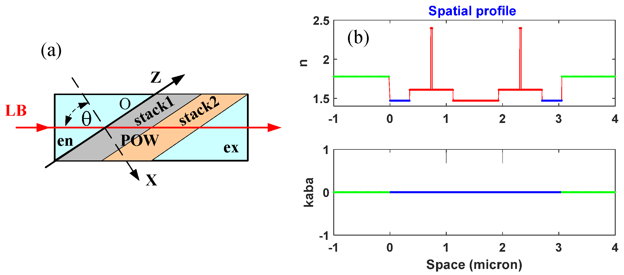
The structure of the proposed OBF is illustrated schematically in
Figure 1a, where X and Z are the coordinate axes, “en” and “ex” denote the two coupling prisms, “POW” stands for the zone where the two planar optical waveguide stacks (“stack1” and “stack2”) are sandwiched, and θ is the angle of the incident light beam (labeled as “LB” in red) at the boundary between the coupling prism “en” and “stack1” of the POW. The inner structure of the waveguide stacks is constructed from the same materials as those in our previous work [
10]. The POW structure in this work consists of nine layers of thin film. The whole POW layers can be functionally simplified as “sub-guiding–gap-guiding cladding” slabs, where the “gap” represents a buffer layer between the two “guiding” slabs. The material refractive index profile along the X axis, i.e., the normal to the POW, is illustrated schematically in
Figure 1b.
The thickness and refractive index for each layer in the POW are represented by d
i and n
i in the simulation model, where i =1…9. Refractive indices of the prism pair are denoted as n
en and n
ex. Light transmission through this stratified structure can be modeled according to the transfer matrix method (TMM) [
20]; the transmittance of amplitude t and of intensity T for the TE polarized light across the POW can be expressed as follows:
where
, N is the total number of layers in the POW, and
,
is the wavelength in vacuum,
is the incident angle, as shown in
Figure 1a. Formulae for the TM wave are similar to Equations (1) and (2) except for parameter
, which is replaced by
in each constituent layer,
, but not for those in the exponents of Equations (1) and (2).
3. Simulations and Results
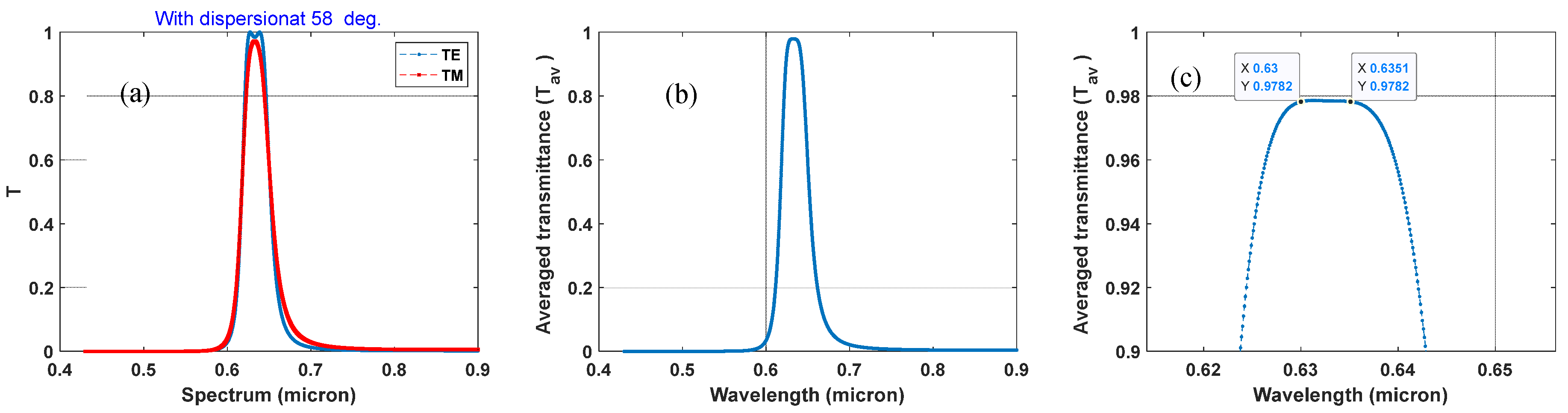
To test the performance of optical filtering in this proposed structure, the transmission matrix method (TMM), Equations (1) and (2) above, was adopted as in our previous design. Numerical simulations were conducted in Matlab R2023a environment. Materials and layer thicknesses in this filter are listed in
Table 1, where the column for the refractive index of each layer gives the representative values at a wavelength of 632.8 nm only. In the simulation process, material dispersions and losses for all the film layers were taken from laboratory data [
10]. The angle of the beam incidence was set to θ = 58.0°, which is above the critical angle (55.85° [
10]) between the “
en” prism and the “sub” layer. Additionally, the transmittances of the two polarization states, TE and TM, were averaged to represent the filtering effect for unpolarized incident light [
21]. These results are shown in
Figure 2a,b, respectively. It is clear that the averaged passband top is flat, although the TE and TM passbands are not completely flat individually. The flat top portion of the unpolarized passband in
Figure 2b is redrawn in
Figure 2c for an enlarged view. The unpolarized passband is designed to be centered at 632.8 nm, the wavelength of the He-Ne laser, for illustration.
To filter the light wave components using the proposed OBF, the light beam “LB” is collimated and it enters the OBF structure at an incident
angle, as shown in
Figure 1a. The refractive indices for the substrate and the cladding layers of the POW should be lower than those of the guiding layers and the two prisms, as shown in
Figure 1b. Furthermore, the incident angle
should be larger than the critical angle at interfaces between the two coupling prisms and at “stack1” and “stack2”, according to the mechanism of prism coupling in the POW [
22].
4. Discussion
From
Figure 2a, it can be seen that with the structural data listed in
Table 1, the simulated two polarized passbands are very symmetric at the 632.8 nm central wavelength, which corresponds to the structure shown in
Figure 1b. Further, they coincide almost exactly upon each other, showing that their FWHM bandwidths are almost the same. Discrepancies between the two bands are minor on the top and at the right foot of the two bands. For the currently optimized data set, there is only one peak in the TM band, whereas there are two peaks in TE band. This result is obtained by the value of the “gap” layer listed in
Table 1, where the two-peak top of the TM band is over-fused, whereas the top of the TE band is still pre-fused and not yet entirely flat. Therefore, the “gap” layer thickness is a key parameter in controlling the passband top of the OBF. Fortunately, during the simulation process, the flatness of the passband in
Figure 2b or
Figure 2c was able to be clearly resolved in a step length of 10 nm for the “gap” layer thickness iterations. This step value is easily controlled with respect to the precision of the film deposition system that was used in our previous sample preparation [
10].
It is clearly seen that the band top illustrated in
Figure 2c remains flat and spans about 5 nm, with transmittance over 97.8%. The FWHM bandwidth of the unpolarized passband in
Figure 2b is about 35 nm, and the two band slopes roll down sharply to the ground almost symmetrically, and the two null sidebands extend almost completely in the visible band, making the passband more or less like a box shape. Comparatively, to obtain an OBF of this passband shape by multiple dielectric films working at 0° incidence, several tens or even hundreds of film layers are necessary [
17].
The POW structure shown in
Figure 1 stems from our previous design, where features of angularly tunable and non-polarizing OBFs were experimentally verified [
10]. In that design guided modes were simultaneously resonant for both TE and TM states. According to optical waveguide theory [
22], guided modes for TE and TM waves in a simple planar optical waveguide, for example, a three-layered POW, can never coincide at the same wavelength due to the phase difference in their respective transcendental equations [
22]. It is the compound guiding slab, which was composed by LHL layers, that provides the opportunity to match the central spectral positions of the TE and TM waves in the resonant passbands. This intuitively ignited the idea that an additional compound “guiding” slab added to the existing one, was able to merge another guided mode in resonance for TE and TM waves to the same central wavelength. By iterating the layer thicknesses in the proposed two waveguide stacks, it was indeed noted that double passbands were formed simultaneously for the TE and TM waves. When the two passbands were shifted sufficiently close, the passbands then began to merge, and the band top became flat in either polarization state of the light. This evolution of the band shape for both polarization states does not have to be at the same rate due to the different phase equations. This may occur as long as another degree of freedom or structural parameter is supplemented.
In the iterations, the thicknesses of the H, L, and “gap” layers played different roles in the spectral positioning and passband shaping. For example, the thickness of the “gap” layer mainly adjusts the spectral distance between the two modes in the individual polarization states. To determine the central wavelength for a certain design of such a non-polarizing POW structure, the iteration roles must be used for the H and L layers in the “guiding” slabs. Fortunately, by establishing a symmetric configuration for the “guiding” slabs, as shown in
Figure 1b, searching for layer parameters for the flat top unpolarized passband on the H and L layers can be made much simpler and easier.
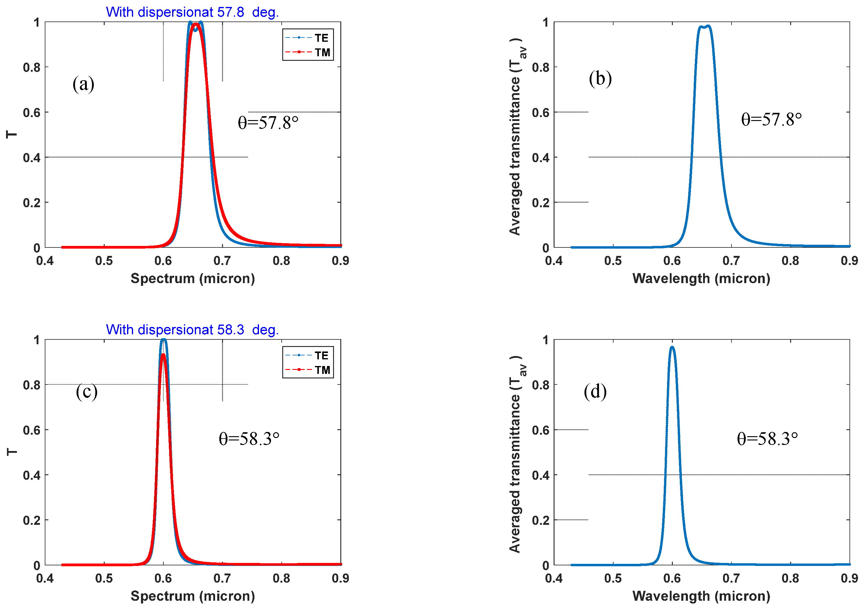
Figure 3 shows the simulation results of angular tolerance for the proposed OBF, at two mistuned incident angles, say 57.8° and 58.3°, respectively, slightly away from the designated central angle of 58.0°. It is seen that at a 0.3° mismatch, the passbands of the TE and TM waves still overlap, so that the unpolarized or non-polarizing passbands still perform well with high transmission efficiency over 96.5%. It is evident from
Figure 3 that within an angular uncertainty of 0.5°, the transmission peak changes only about 1%. Additionally, the passband shape distortions are small. This is very useful for practical device applications, for example, in optical sensing [
23]. Spectroscopic properties, such as central wavelength, peak transmittance, and bandwidth of the passbands for the TE, TM, and averaged non-polarizing passbands shown in
Figure 2 and
Figure 3, are summarized in
Table 2.
To make a comparison, performances of our proposed OBF and other reported thin-film-based OBFs are summarized in
Table 3. It is clear that the number of film layers in our proposed OBF is the minimum, while the three important features of flat top, non-polarizing, and tunable are still maintained. In addition, the band top ripple can also remain very low.
Comparatively, the advantages of our proposed OBF are evident over OBFs made from dielectric thin films working at 0° incidence, and also over those made from one- or two-dimensional waveguide gratings [
27,
28]. Firstly, the non-polarizing filtering designed with only five layers of thin-film layers has been experimentally demonstrated. The flatness of the band top as simulated in this work with a film stack of only nine layers originates from the fusion of two guided-mode resonances in the planar waveguide. When these two modes are merged or fused, it ensures the resonances of a series of wavelengths so that makeing the passband top flat instead of single peaked. Secondly, because of the guided mode resonance, off-resonant wavelengths are prevented from entering the guiding region; thus, the number of film layers needed for constructing a flat top and non-polarizing filter is greatly reduced. And thirdly, the processing for device fabrication of this OBF type involves only planar thin film depositions without any complicated lithographic steps, which are required for waveguide grating OBFs [
27,
28].
5. Conclusions
In this work, based on our previous experimentally verified design of a polarization-independent bandpass filter, we present a new structure that provides a flat top and non-polarizing optical bandpass filter. This new design includes two planar optical waveguide stacks with only nine thin-film layers, making this type of OBF more effective in terms of device fabrication and cost reduction. Theoretical simulations demonstrated the high transmission efficiency and structural tolerance. Therefore, this type of OBF has prominent potential for many applications in optical and laser spectroscopies.
Although performing well when theoretically simulated in the visible spectral region, additional effort is needed on more accessible bandwidths, either wider or narrower, and more central wavelengths, especially to the longer side of the spectrum, such as the NIR communication bands. In addition, experimental studies also have to be conducted to facilitate actual potential applications.

