Abstract
This article presents a novel Ka-band Marchand balun implemented in 0.13-μm SiGe bipolar complementary metal–oxide–semiconductor (BiCMOS) process. By combining both edge- and broadside-coupled structures, the new hybrid balun is able to increase the coupling and minimize the balun insertion loss. As compared with conventional edge-coupled or broadside-coupled structures, the proposed balun achieves the lowest insertion loss of 1.02 dB across a wide 1-dB bandwidth from 29.0 GHz to 46.0 GHz, with a core size of 270 μm 280 μm.
1. Introduction
Balun, which converts single ended signals into balanced signals is widely used in RF front-end modules, such as frequency multipliers, mixers which utilize differential signals for common-mode signal cancellation, and to improve port isolations. Key performance specifications of a balun include insertion loss, amplitude/phase balance, and chip size. These parameters are important in the design of millimeter-wave (MMW) circuits and systems [1]. Marchand balun [2,3,4,5,6,7,8,9,10], which utilizes two coupled line sections, is widely used in MMW frequency circuit design, due to its wide operating bandwidth and easy implementation.
In [2], an asymmetric broadside coupled Marchand balun based on the modified off-center frequency method was proposed. It achieves a bandwidth of 34–110 GHz; however, it suffers from high insertion loss averaging around 3 dB. Another 30 GHz to 60 GHz transformer balun [11] with offset radii coils was designed to address imbalance performance. Results show a low-amplitude imbalance of 0.12 dB and phase imbalance of less than 1°; however, the maximum insertion loss is around 3 dB. A miniaturized on-chip Marchand balun [12], based on a stacked-spiral-coupled (SSC) structure with a self-coupled compensation line and center-tapped ground-shield with deep trench, was designed for wideband operation from 6.5 GHz to 28.5 GHz, but a maximum of 3 dB insertion loss was measured. Wideband operation and amplitude/phase imbalance had been the focus of previous reported literature, with the trade-off of balun insertion loss. In this article, the design of a novel Ka-band Marchand balun with low insertion loss is presented, while achieving wideband operation with acceptable imbalance performance. The proposed balun employs both edge- and broadside-coupled combined structures to enhance the coupling between the primary and secondary signals and, thus, achieves a measured low insertion loss of 1.02 dB across a 1 dB bandwidth from 29.0 GHz to 46.0 GHz. Section 2 presents the detailed balun analysis and proposed balun design, Section 3 discusses the experiment results and makes a comparison with the state-of-the-art, and Section 4 draws the conclusion.
2. Design of the Proposed Balun
2.1. Technology
A high-performance bipolar complementary metal–oxide–semiconductor (BiCMOS) technology (SG13G2) with a 0.13-μm complementary metal–oxide–semiconductor (CMOS) process from innovations for high performance microelectronics (IHP) has been used for designing the balun. The backend of the line offers 5 thin metal layers, metal 1 (M1) to metal 5 (M5), two thick metal layers, top metal 1 (TM1, 2 μm thick) and top metal 2 (TM2, 3 μm thick), and a metal–insulator–metal (MIM) layer.
2.2. Balun Analysis
Figure 1 shows the schematic of the conventional Marchand balun, which consists of two identical coupled line sections, where a single section coupler with electrical length of θ, is shown in Figure 2, and its four-port S-parameter matrix can be represented by Equation (1), as given in [13].
where , , and , and is the coupling coefficient.
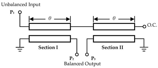
Figure 1.
Block diagram of the conventional Marchand balun.
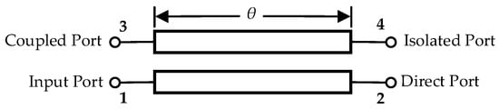
Figure 2.
A single section coupler.
Then from [9], the insertion loss of the Marchand balun can be derived as
Ideally balanced output ports P2 and P3 should be of equal magnitude and exactly 180° out of phase. The plot of the insertion loss S21 as a function of electrical length θ, for different values of coupling coefficient , is shown in Figure 3. It is observed that the insertion loss initially decreases as increases; further increasing beyond 0.7 will increase the insertion loss at the center frequency , while the flattest frequency response occurs for between 0.6 and 0.7. Based on the above observation, the balun insertion loss can be minimized through optimizing the coupling coefficient , as presented in this work. Figure 4 shows the schematic of the designed Marchand balun with a capacitor C1 added to connect the open circuit (O.C.) port to ground, so as to reduce the coupled transmission line length, as well as achieve good in-band matching.
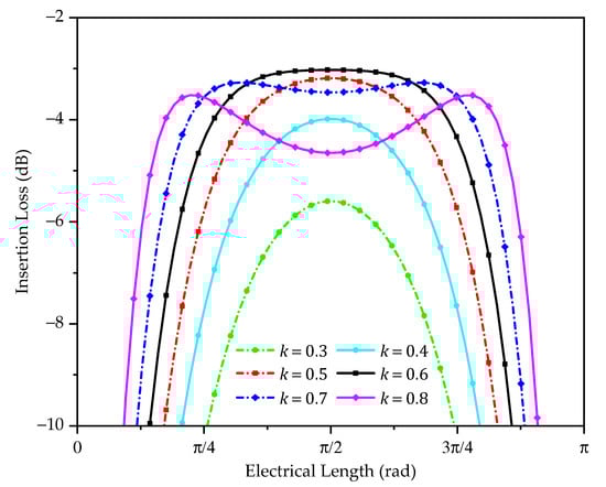
Figure 3.
Plot of insertion loss versus the coupled line electrical length θ, for different coupling coefficient .
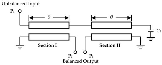
Figure 4.
Block diagram of the designed Marchand balun with capacitive termination.
Meander lines with a 45° bend have been used to save chip area. To reduce the insertion loss, the top two thick metal layers, TM1 and TM2, with low sheet resistance and low parasitic capacitances to substrate are used. A Metal 1 to TM2 guard-ring surrounding the balun is drawn and shorted by internal Vias to ground and is connected to the substrate through contact Vias, as shown in Figure 5a.
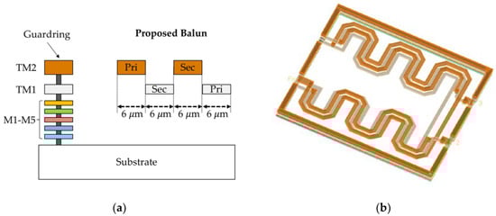
Figure 5.
(a) Cross-section view of the metal stack and proposed balun; (b) 3D view of the balun.
2.3. Proposed Balun
The proposed balun structure is shown in Figure 5. Broadside-coupling between TM1 and TM2 layers and edge-coupling in both TM1 and TM2 layers is formed between primary and secondary signals. Further optimization using Keysight Advanced Design System’s (ADS) Momentum Electromagnetic (EM) simulator was performed to obtain the optimum metal width and spacing, with a 6 μm metal width and a 6 μm metal spacing obtained for both TM1 and TM2 layers, as shown in Figure 5a. Detailed analysis for the proposed balun is given in Figure 6 with the cross-sectional view shown in Figure 6a, where and are the TM1 and TM2 conductor capacitance to ground, respectively. and are the mutual capacitances for the edge-coupled TM1 and TM2, respectively, and is the mutual capacitance between the broadside-coupled TM1 and TM2. Figure 6b shows the equivalent simplified model of the balun, and the corresponding even/odd mode models are given in Figure 6c, Figure 6d, respectively.
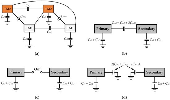
Figure 6.
(a) Cross-section of the proposed balun; (b) simplified model of the proposed balun; (c) even mode analysis; (d) odd mode analysis.
Then from [13], the coupling coefficient can be expressed as
where , and . Therefore, increases as increases. Compared with the edge-coupled structure, where either or exists, or the broadside-coupled structure with only mutual capacitance , using the proposed edge- and broadside-coupled hybrid configuration, a higher can be obtained, hence maximizing coupling .
Using 6 μm metal width for both primary and secondary coupled lines, for the edge-coupled structure, the coupling is limited by the minimum metal spacing rule defined by the foundry process, with a highest simulated of 0.57; for the broadside-coupled structure, it is limited by the vertical distance between TM1 and TM2, with a highest simulated of 0.61. With the proposed edge- and broadside-coupled hybrid structure, a coupling of 0.62 is achieved. Further optimizing the capacitive termination, capacitance in Figure 4 with 30 fF for both edge- and broadside-coupled structures and 74 fF for the proposed hybrid balun, the simulated insertion loss is shown in Figure 7. It can be seen that the proposed balun has achieved the lowest minimum insertion loss among all the designs.
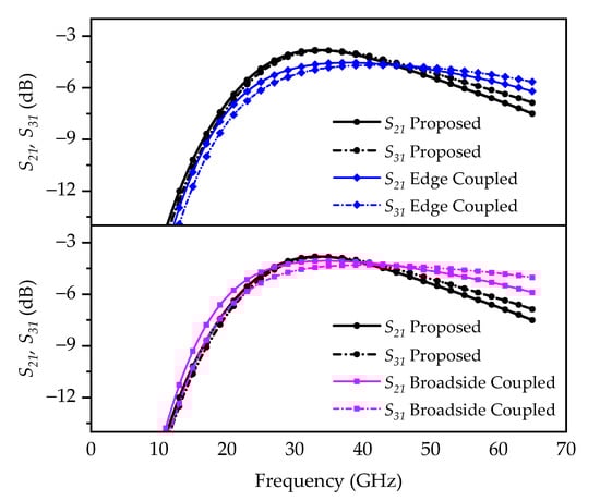
Figure 7.
Plot of insertion loss.
By transforming the three-port balun into a two-port network, the minimum insertion loss ILmin [14] can be calculated by Equations (4) and (5), and the calculated ILmin is shown in Table 1. Simulation and calculation results correlate well, showing that the proposed hybrid structure gives the minimum insertion loss.

Table 1.
Simulated and calculated ILmin *.
From [13], the equivalent even/odd mode characteristic impedance and can be expressed as
where is the mutual inductance, and is the mutual capacitance and is equal to in the proposed balun.
Then from [15], the amplitude imbalance of the balun can be written as
From Equations (6)–(8), it can be seen that, as the coupling coefficient increases, both the mutual inductance, and mutucal capacitance, increase, and thus, decreases, increases, and the amplitude imbalance shifts towards the ideal 0 dB. Figure 8 shows the simulated amplitude and phase imbalance, where phase imbalance is defined as
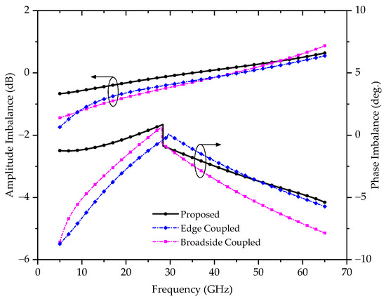
Figure 8.
Plot of amplitude and phase balance.
From Figure 8, it can be seen that the proposed balun shows significant improvement over the conventional edge-coupled and broadside-coupled structures in terms of amplitude/phase balance, where the amplitude and phase imbalance are −0.18 dB to 0.20 dB and −3.23° to 0.81°, respectively across a 1-dB frequency bandwidth.
3. Experiment Results
The proposed balun is fabricated using the IHP 0.13-μm SiGe BiCMOS process with a core size of 270 μm 280 μm. The on-wafer measurement is carried out using the Keysight PNA-X network analyzer N5247A (Keysight, Santa Rosa, CA, USA) with a four-port Hybrid Line–Reflect–Reflect–Match (LRRM) and Short–Open–Load–Thru (SOLR) calibration. The measurement setup and die photo is shown in Figure 9. A minimum insertion loss of 1.02 dB with a 1-dB bandwidth of 29.0 GHz to 46.0 GHz is measured, as shown in Figure 10.
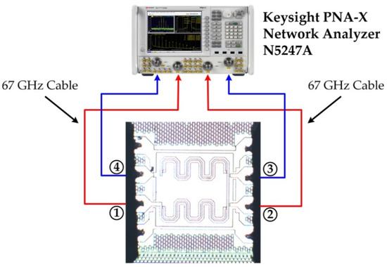
Figure 9.
Measurement setup.
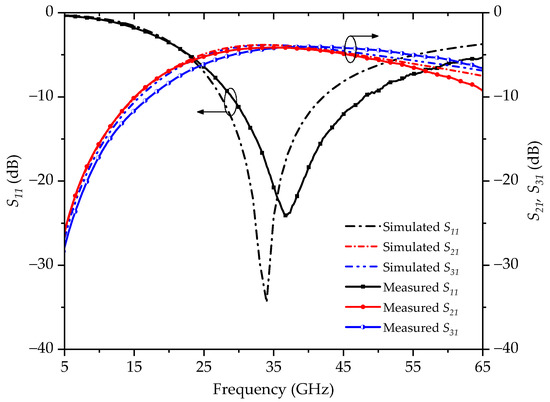
Figure 10.
Simulated and measured performance of the proposed balun.
Figure 11 shows the simulated and measured amplitude and phase imbalances. A ±0.83 dB amplitude imbalance and −3.8° to −7.3° phase imbalance is measured across the band from 29.0 GHz to 46.0 GHz. The small difference between the simulated and measured data is primarily due to the imbalance introduced between the output differential ports during the calibration phase. In addition, the measured frequency shift is due to the process variation of the capacitor C1.
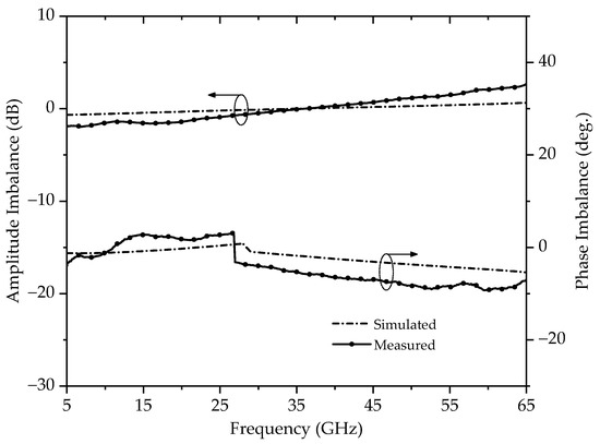
Figure 11.
Simulated and measured amplitude and phase imbalance.
Common mode rejection ratio (CMRR), defined as the ratio between the differential-mode insertion loss over the common-mode insertion loss as shown in Equation (10), is plotted in Figure 12. CMRR more than 25 dB has been measured for the proposed hybrid structure. The difference between simulated and measured data is due to higher amplitude and phase imbalance, as the CMRR is dependent on the amplitude and phase balance of the balun. Poor amplitude or phase balance will result in higher common-mode signal pass through and, thus, low CMRR.
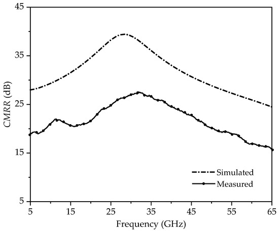
Figure 12.
Simulated and measured common mode rejection ratio (CMRR).
Finally, Table 2 shows the measured performance comparison with the reported SiGe baluns. Compared with the reported standalone broadside-coupled baluns, the proposed hybrid structure has achieved a lowest insertion loss of 1.02 dB.
Table 2.
Performance comparison with reported baluns.
4. Conclusions
In this article, the influence of the coupling coefficient on the Marchand balun insertion loss has been studied. As coupling for the stand-alone edge-coupled and broadside-coupled structures has reached the process limitation, a new structure combining both edge-coupled and broadside-coupled configurations is proposed to enhance the coupling and therefore increase to minimize the insertion loss. With that, a good amplitude imbalance of ±0.83 dB and measured insertion loss of 1.02 dB has been obtained across a 1-dB bandwidth from 29.0 GHz to 46.0 GHz.
Author Contributions
Conceptualization, J.Y.; methodology, J.Y.; validation, J.Y. and K.M.; resources, K.S.Y.; writing—original draft preparation, J.Y.; writing—review and editing, H.L. and K.S.Y.; supervision, H.L.; funding acquisition, X.Z. All authors have read and agreed to the published version of the manuscript.
Funding
This research was funded by Singapore National Research Foundation, award number NRF-CRP20-2017-0003 and project number CRP20-2017-0006.
Conflicts of Interest
The authors declare no conflicts of interest.
References
- Yang, G.; Wang, Z.; Li, Z.; Li, Q.; Liu, F. Balance-Compensated Asymmetric Marchand Baluns on Silicon for MMICs. IEEE Microw. Wirel. Compon. Lett. 2014, 24, 391–393. [Google Scholar]
- Song, I.; Schmid, R.L.; Howard, D.C.; Jung, S.; Cressler, J.D. A 34–110 GHz wideband, asymmetric, broadside-coupled Marchand balun in 180 nm SiGe BiCMOS technology. In Proceedings of the 2014 IEEE MTT-S International Microwave Symposium (IMS2014), Tampa, FL, USA, 1–6 June 2014. [Google Scholar]
- Zhang, J.; Ye, Y.; Sun, X.W. A W-band high conversion gain, single-balanced subharmonically gate-pumped mixer with novel size-reduced Marchand balun. In Proceedings of the 2015 IEEE MTT-S International Microwave Symposium, Phoenix, AZ, USA, 17–22 May 2015. [Google Scholar]
- Xu, L.; Sjoland, H.; Törmänen, M.; Tired, T.; Pan, T.; Bai, X. A Miniaturized Marchand Balun in CMOS With Improved Balance for Millimeter-Wave Applications. IEEE Microw. Wirel. Compon. Lett. 2014, 24, 53–55. [Google Scholar] [CrossRef]
- Tsai, P.; Lin, Y.-H.; Kuo, J.-L.; Tsai, Z.-M.; Wang, H. Broadband Balanced Frequency Doublers With Fundamental Rejection Enhancement Using a Novel Compensated Marchand Balun. IEEE Trans. Microw. Theory Tech. 2013, 61, 1913–1923. [Google Scholar] [CrossRef]
- Chiou, H.K.; Lin, J.Y. Symmetric Offset Stack Balun in Standard 0.13-um CMOS Technology for Three Broadband and Low-Loss Balanced Passive Mixer Designs. IEEE Trans. Microw. Theory Tech. 2011, 59, 1529–1538. [Google Scholar] [CrossRef]
- Xu, Z.; MacEachern, L. Optimum Design of Wideband Compensated and Uncompensated Marchand Baluns With Step Transformers. IEEE Trans. Microw. Theory Tech. 2009, 57, 2064–2071. [Google Scholar]
- Chiou, H.; Yang, T. Low-Loss and Broadband Asymmetric Broadside-Coupled Balun for Mixer Design in 0.18-mm CMOS Technology. IEEE Trans. Microw. Theory Tech. 2008, 56, 835–848. [Google Scholar] [CrossRef]
- Lin, C.S.; Wu, P.-S.; Yeh, M.-C.; Fu, J.-S.; Chang, H.-Y.; Lin, K.-Y.; Wang, H. Analysis of Multiconductor Coupled-Line Marchand Baluns for Miniature MMIC Design. IEEE Trans. Microw. Theory Tech. 2007, 55, 1190–1199. [Google Scholar] [CrossRef]
- Jia, H.; Chi, B.; Kuang, L.; Wang, Z. A W-Band Power Amplifier Utilizing a Miniaturized Marchand Balun Combiner. IEEE Trans. Microw. Theory Tech. 2015, 63, 719–725. [Google Scholar] [CrossRef]
- Chakraborty, S.; Milner, L.E.; Hall, L.T.; Parker, A.; Heimlich, M. A 30–60 GHz SiGe transformer balun with offset radii coils for low amplitude and phase imbalance. In Proceedings of the 2017 IEEE MTT-S International Microwave Symposium (IMS), Honololu, HI, USA, 4–9 June 2017. [Google Scholar]
- Qian, H.J.; Luo, X. Compact 6.5-28.5 GHz On-Chip Balun With Enhanced Inband Balance Responses. IEEE Microw. Wirel. Compon. Lett. 2016, 26, 993–995. [Google Scholar] [CrossRef]
- Mongia, R.; Bhartia, P.; Bahl, I.J. RF and Microwave Coupled-Line Circuits; Artech House: Norwood, MA, USA, 2007. [Google Scholar]
- Leite, B. Design and Modeling of mm-Wave Integrated Transformers in CMOS and BiCMOS Technologies 2012. Ph.D. Thesis, University of Bordeaux 1, Talence, France, 2012; p. 162. [Google Scholar]
- Hsu, H.; Huang, J.-S.; Chen, S.-Y.; Lai, S.-H. Design of an On-Chip Balun With a Minimum Amplitude Imbalance Using a Symmetric Stack Layout. IEEE Trans. Microw. Theory Tech. 2010, 58, 814–819. [Google Scholar]
- Ma, K.; Yan, N.; Yeo, K.S.; Lim, W.M. Miniaturized 40–60 GHz On-Chip Balun With Capacitive Loading Compensation. IEEE Electron Device Lett. 2014, 35, 434–436. [Google Scholar] [CrossRef]
© 2020 by the authors. Licensee MDPI, Basel, Switzerland. This article is an open access article distributed under the terms and conditions of the Creative Commons Attribution (CC BY) license (http://creativecommons.org/licenses/by/4.0/).