Article

Design of Differential Variable-Gain Transimpedance Amplifier in 0.18 µm SiGe BiCMOS

1
Engineering Product Development, Singapore University of Technology and Design, 8 Somapah Road, Singapore 487372, Singapore
2
College of Information Science and Electronic Engineering, Zhejiang University, 866 Yuhangtang Road, Xihu District, Hangzhou 310027, China
*
Author to whom correspondence should be addressed.
Electronics 2020, 9(7), 1058; https://doi.org/10.3390/electronics9071058
Submission received: 8 May 2020 / Revised: 16 June 2020 / Accepted: 20 June 2020 / Published: 27 June 2020
(This article belongs to the Special Issue Millimeter-Wave Integrated Circuits and Systems for 5G Applications)

Abstract

:
This paper presents two new inductorless differential variable-gain transimpedance amplifiers (DVGTIA) with voltage bias controlled variable gain designed in TowerJazz’s 0.18 µm SiGe BiCMOS technology (using CMOS transistors only). Both consist of a modified differential cross-coupled regulated cascode preamplifier stage and a cascaded amplifier stage with bias-controlled gain-variation and third-order interleaving feedback. The designs have wide measured transimpedance gain ranges of 24.5–60.6 dBΩ and 27.8–62.8 dBΩ with bandwidth above 6.42 GHz and 5.22 GHz for DVGTIA designs 1 and 2 respectively. The core power consumptions are 30.7 mW and 27.5 mW from a 1.8 V supply and the input referred noise currents are 10.3 pA/√Hz and 21.7 pA/√Hz. The DVGTIA designs 1 and 2 have a dynamic range of 40.4 µA to 3 mA and 76.8 µA to 2.7 mA making both suitable for real photodetectors with an on-chip photodetector capacitive load of 250 fF. Both designs are compact with a core area of 100 µm × 85 µm.

1. Introduction

The demand for data transmission will increase immensely in the future due to applications such as cloud-computing and the internet of things, causing an insufficient capacity for the current Wi-Fi frequency channels used. Currently, the millimeter wave band is being taken and developed for the 5G communication network. Hence, visible light communication (VLC) offers another solution as the unused visible light spectrum (400 THz–800 THz) can also be used for wireless communication due to the dwindling available RF spectrum [1,2]. The light signal can be transmitted through short distances via light-emitting diodes (LEDs) or long distances via fiber optic cables which are deployed across the world [1,2]. Data is transmitted by modulating the light signal through controllable LEDs [1,2]. The key advantages of VLC include the fact that light signals can be easily confined within opaque walls, thus keeping data transmission secure within a room, rapid replacement of fluorescent lighting to LED lighting as well as the low costs of the LEDs themselves [1,2]. This allows them to be well-suited for a wide variety of near-field wireless communication applications such as secure office/home and vehicle-to-vehicle or vehicle-to-traffic-light communication [1,2].
The transimpedance amplifier (TIA) is a chip block that converts and amplifies current input signal into voltage output [1,2,3]. Other than for VLC, TIAs can also be utilized in other applications such as magnetic resonance imagining for healthcare, infra-red night vision and even sensors, such as accelerometers and gyroscopes, that have microelectromechanical systems (MEMS) components as long as there is a current signal output to input into the TIA [3]. However, as different applications require different design specifications [3], this paper focuses on TIA designs for VLC.
The VLC transceiver consists of a transmitter and a receiver module with the transmitter having a photodiode and the receiver having a photodetector to transmit and receive the light signal respectively [3,4,5,6,7]. A key limitation of VLC systems is the low efficiency of the electro-optical conversion for the photodiode and vice versa which is solved by improvements in LED efficiency as well as the need for larger photodetectors in the receiver to absorb sufficient light [1,2]. In the receiver module, the TIA is the first circuit block after the photodetector that converts its current output into voltage [4,5,6,7]. As the first block, the TIA determines important parameters such as the bandwidth, noise, sensitivity and dynamic range, for subsequent blocks and thus, for the entire VLC system [3,4,5,6,7]. Silicon-based processes, such as the complementary metal-oxide semiconductor (CMOS) and Silicon–Germanium (SiGe), have been widely used for previous TIA designs due to the fact of its technological maturity, low-cost, high reliability at high frequency and on-chip integrability with photodiodes and photodetectors [4,5,6,7]. Both CMOS and bipolar-junction transistors (BJTs) can be made together on the same chip in a SiGe BiCMOS process.
The major challenge for TIA designs is to overcome the gain–bandwidth trade-off, with the bandwidth limited by the large photodetector parasitic capacitive load ( C p d ) that drags down the frequency of the dominant pole located at the TIA input. Thus, most TIA designs try to compensate C p d by lowering the input impedance Z i n of the TIA design [4,5,6,7,8]. A popular technique to do this is through the regulated cascode (RGC) design [4,5,6,7], while additional bandwidth-enhancing techniques, such as interleaving feedbacks [6,7], capacitive degeneration [7] and active-inductive peaking [8], are also common to introduce zeros to counter the dominant pole. Another technique is to use parallel pathways, such as via PMOS transistors, from the input to increase transconductance at input and, thus, lower Z i n [6,8]. To keep the TIA size small and, thus, low cost, an inductorless design is always preferred as on-chip inductors are large in physical size [4,5,6,7,8].
A differential design is also advantageous over a single-ended design for three reasons. Firstly, the common-mode noise would be cancelled [7,8]. Secondly, other types of noise such as power supply and substrate-coupling noise would be lowered [7,8]. Thirdly, it would not require a large AC-eliminating capacitor within the single to differential converter in order to input a required differential signal into the limiting amplifier (LA) block after the TIA [7,8].
In order to increase the dynamic range of the input signal, the amplifier should have a variable gain function in order to lower the gain when the input signal is high to prevent gain compression and thus non-linearity of the output signal [5,7]. This is because the input signal strength from a usual photodetector with typical responsivity and optical modulation index has a large input signal current range of 150 µA to 0.9 mA due to the variable user-required optical power from −6 to 2 dBm [7,9].
The variable-gain function can use gain-varying techniques from variable-gain amplifier (VGA) designs. Previous papers have explored having voltage-controlled gain varying transistors in the load of common-source amplifiers [10,11,12] with separate PMOS and NMOS pathways for dB-linearity [11,12] as well as reconfigurable DC-offset cancellation to remove DC differences between both differential sides [13]. Ideally, when varying gain, the gain-controlling pole and peaking-controlling zero should be adjusted together to ensure a flat frequency response and prevent instability [11,12].
The proposed inductorless differential variable-gain TIA (DVGTIA) in this paper builds on the authors’ previous design in [7], with measurement results from the taped-out chips presented here. Two similar designs are shown, both consisting of a novel cross-coupled regulated cascode input stage and a gain-varying gain stage. The designs are unique for several reasons. Firstly, they take a single-ended input with a single C p d to become a differential output while maintaining the low input impedance of a RGC configuration. Secondly, they have an additional automatic small negative feedback at the input to lower input impedance even further. The bandwidth is maintained throughout the gain stage by using interleaving feedback and capacitive degeneration. Although the designs are taped-out in TowerJazz’s 0.18 µm SiGe BiCMOS technology, only CMOS transistors are used and thus they are compatible with a normal bulk CMOS process [7].
This paper is organized as such. Section 2 discusses the literature review of previous TIA designs and design techniques. Section 3 discusses the two proposed TIA designs in this paper, their design novelty, layout and measurement setup. Section 4 presents the post-layout simulation before chip tape-out as well as the measurement results after chip tape-out. Section 5 discusses the results in Section 4 and compares them with other recent papers and finally Section 6 is the conclusion.

2. Literature Review

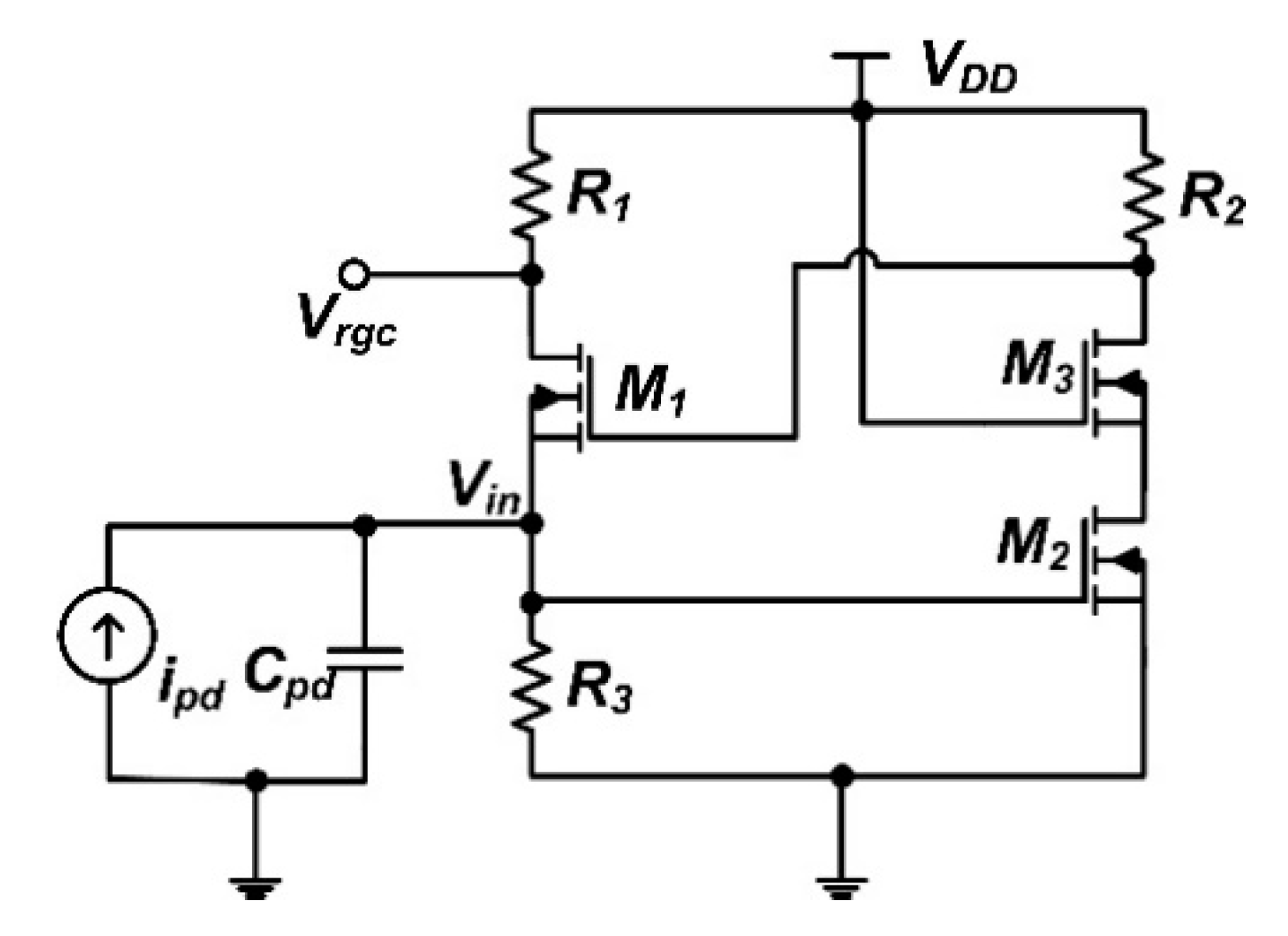
2.1. Regulated Cascode TIA

The goal of a TIA design is to lower the input impedance Z i n as much as possible and thus the simplest TIA design is a common-gate (CG) with a Z i n of 1/ g m [4,5,6,7], where g m is the transconductance of the transistor. As shown in Figure 1, an active photodetector is modelled with a C p d load and current input i p d into the TIA input at V i n . The regulated cascode (RGC) is a popular TIA design as the internal feedback allows M 1 to act as both a CG and common-source (CS) amplifier, lowering Z i n further to 1/ g M 1 ( 1 + g M 2 R 2 ) .
The additional cascode transistor M 3 helps to eliminate the Miller effect that arises due to the CS M 2 transistor by increasing the separation between the input V i n from the output V r g c [6,7], thus helping to increase the bandwidth while having little impact on the gain of RGC TIA. The transimpedance gain Z T , R G C and the poles are calculated as [7]:
Z T , R G C =   V r g c V i n =   R 1 ( 1 + s ω p 1 ) ( 1 + s ω p 2 )
ω p 1 = 1 { R 3 | | ( r o M 1 + R 1 ) } ( C p d + C i )   ,    ω p 2 =   1 R 1 | | ( r o M 1 + R 3 ) C o
where pole ω p 1 is located at V i n , pole ω p 2 is located at V r g c , C i and C o are the capacitive loads of the transistors at V i n and V r g c respectively. The problem with this RGC TIA design is that the dominant pole ω p 1 is still located at V i n due to the insufficient lowering of Z i n for a typical C p d value such as 250 fF, causing C p d to still have a significant impact on the bandwidth of the TIA. Thus, further modification on the RGC is required to further lower Z i n and isolate C p d from bandwidth determination [4,5,6,7].

2.2. Cross-Coupling TIA

Apart from just one feedback in the RGC TIA design, there could be a cross-coupled design as shown in Figure 2 with dual feedbacks to the gates of M 1 A | 1 B in order to create more zeros and increase the bandwidth as in [14].
Care must be taken to ensure that the dual feedback loops do not cause instability shown by frequency response peaking and, thus, resulting in oscillation of the amplifier. R 1 A | 1 B contributes to both the gain of the TIA as well as to the feedback gain. Hence, to prevent instability and oscillation, the value of R 1 A | 1 B and thus the gain is limited. Another disadvantage of this design is that it does not have a differential output.
The cross-coupling design can also be made to be a differential design shown in Figure 3 as in [15]. In this design, components of both sides are identical in size to equalize the DC voltages at V o u t + and V o u t . Since the cross-coupling is also a dual feedback, it likewise helps to generate the opposite small-signal of V o u t + at V o u t although it is not yet entirely equal in magnitude.
However, a key disadvantage is that the input of both sides is a simple CG with a higher Z i n of 1/ g M 1 (without considering the cross-coupling) since there is no CS circuit directly from the input. Furthermore, there is an entire dummy circuit with an additional large C p d on the side without the input signal which both wastes chip area and reduces bandwidth. Lastly, precious voltage headroom is wasted by adding M 2 as a cascode yet simply biasing it with a fixed V B I A S , effectively limiting the gain to reduce the Miller effect. Thus, although the output is a differential signal, it is more costly in terms of price, gain and bandwidth.

3. Design Process of Proposed DVGTIA

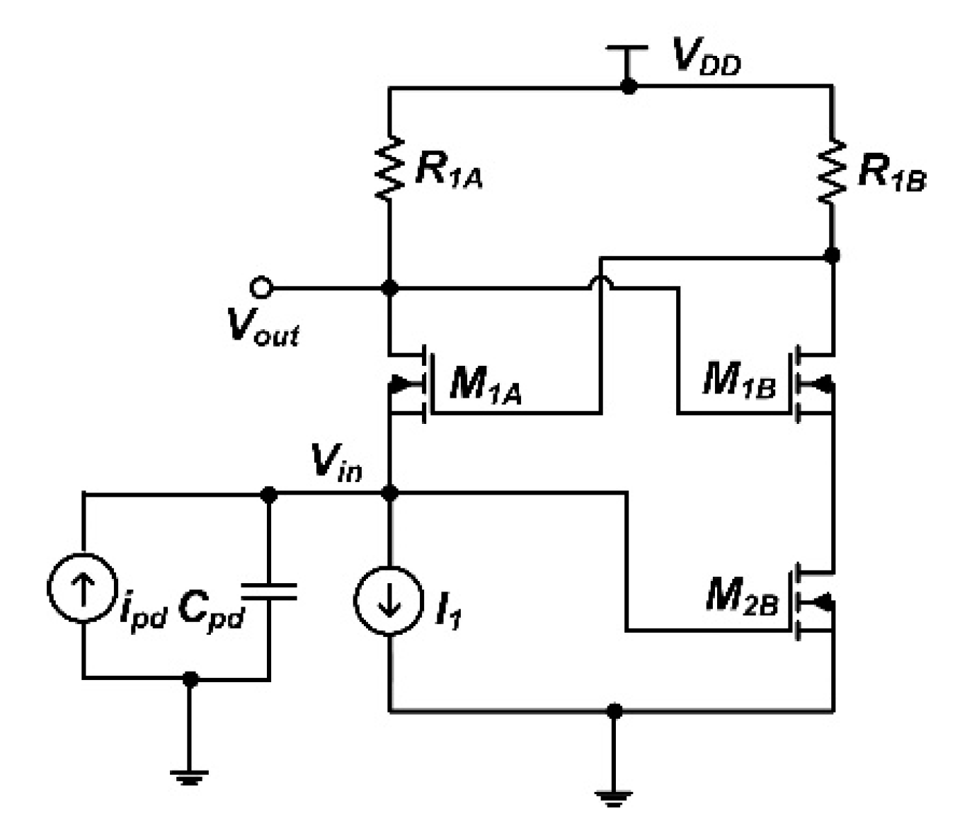
3.1. Proposed Input Stage of the DVGTIA Design

The proposed DVGTIA input stages shown in Figure 4 is similar to the authors’ previous design in [7], with added feedback transistors M 3 A | 3 B and M 4 A | 4 B for designs 1 and 2 respectively. It is a cross-coupled design similar to [14], but it uniquely takes a single-ended input with a single C p d to become a differential output while maintaining the low Z i n RGC configuration unlike in [15].
The transistors M 1 A | 1 B act as both a CG and CS, with the input signal just from a single side V i n while M 1 B is still able to be a cascode transistor for the CS M 2 B . R 1 A | 1 B determines the gain of the input stage while R 2 determines the peaking of the frequency response. This is done because it controls the difference in input signal between M 2 A | 2 B , whereby M 2 A is the biasing of the M 1 A CG and M 2 B is CS of the opposite side. Because there are only three components in the V D D instead of four unlike in [15] while still maintaining the cascode configuration, this allows for greater voltage headroom across the gain resistor R 1 A | 1 B and thus, increases gain for the TIA. Even though the functions of transistors on both sides are different, they are the same size to equalize DC similar to [15].
An additional novelty is that there is an automatic small negative feedback in both designs back to the input at V i n that introduces another zero at V i n and lowers Z i n further, compensating the large C p d load and increasing the bandwidth. As shown in Figure 4, the difference in designs 1 and 2 is that for design 1, the feedback is directly from V m i d + and V m i d to the gates of M 3 A | 3 B , while in design 2, it is from the nodes V g 2 and V g 2 + respectively, in the gain stage. For design 1, the advantage is that the feedback path is shorter in layout since it is from the same stage at V m i d , yet this would cause additional parasitic capacitance at V m i d which is a more sensitive node along the signal path than V g 2 . Conversely, for design 2, the feedback has a longer path in layout yet does not burden V m i d . Although the difference seems minor, it affects the location of the poles and zeros, hence, affecting the frequency response in which would be shown later.
The calculated Z i n ( 0 ) of the first DVGTIA input stage is:
Z i n , D V G T I A = 1 g M 1 A × 1 ( 1 + g M 2 B R 1 B ) ( 1 + g M 3 A R 1 A )
where g M 1 A | 1 B = 11 m S , g M 2 A | 2 B = 8.5 m S , g M 3 A | 3 B g M 4 A | 4 B 1 m S from simulation results. Both designs 1 and 2 do not have very different Z i n . Hence, the calculated Z i n , D V G T I A is lower than Z i n , R G C .
To find the input stage gain, the transfer functions of all feedback loops are listed in Table 1:
Hence, by identifying and combining all feedback loops and taking V i n = I i n × Z i n , transimpedance gain Z T , i n of the first DVGTIA input stage positive side Z T , i n 1 + and negative side Z T , i n 1 is calculated as loops from V i n to V m i d + : loop 1: V m i d + V i n , loop 2: V i b V i n × V m i d V i b × V m i d + V m i d , −loop 3: V i n V m i d + :
Z T , i n 1 + * =   Z i n × V m i d + V i n = | 1 + g M 1 B R 1 B g M 1 B R 1 B g M 3 A R 1 A g M 1 A ( 1 + g M 2 B R 1 B ) ( 1 + g M 3 A R 1 A ) |
*Note that since the signals at V i n and V m i d + have the same sign, the absolute value is taken for Z T , i n 1 + .
Loops from V I N to V m i d : loop 1: V m i d V i n , loop 2: V i b V i n × V m i d V i b , loop 3: V m i d + V i n × V m i d V m i d + , −loop 4: V i b * V m i d :
Z T , i n 1 * =   Z i n × V m i d V i n = | 1 + g M 1 B R 1 B + g M 1 A R 1 A g M 3 B R 1 B g M 1 A ( 1 + g M 2 B R 1 B ) ( 1 + g M 3 A R 1 A ) |
*Note that the negative loop is taken from V i b instead of V i n for simplification as A C S , M 2 B is only one-directional, i.e., V i n / V i b does not exist. Also, since the signals at V i n and V m i d are opposite in phase, thus the negative of the absolute value for Z T , i n 1 is taken.
For the second DVGTIA input stage Z T , i n 2 + and Z T , i n 2 , the transistors for the negative loops are M 4 A | 4 B instead of M 3 A | 3 B and the transfer functions are substituted accordingly:
Z T , i n 2 + =   Z i n × V m i d + V i n = | 1 + g M 1 B R 1 B g M 1 B R 1 B g M 4 A R 1 A g M 1 A ( 1 + g M 2 B R 1 B ) ( 1 + g M 4 A R 1 A ) |
Z T , i n 2 =   Z i n × V m i d V i n = | 1 + g M 1 B R 1 B + g M 1 A R 1 A g M 4 B R 1 B g M 1 A ( 1 + g M 2 B R 1 B ) ( 1 + g M 4 A R 1 A ) |
The differential gain is the difference between both gains which are of opposite polarities, hence the absolute values are added together to get Z T , i n 1 , d i f f and Z T , i n 2 , d i f f of DVGTIA designs 1 and 2.

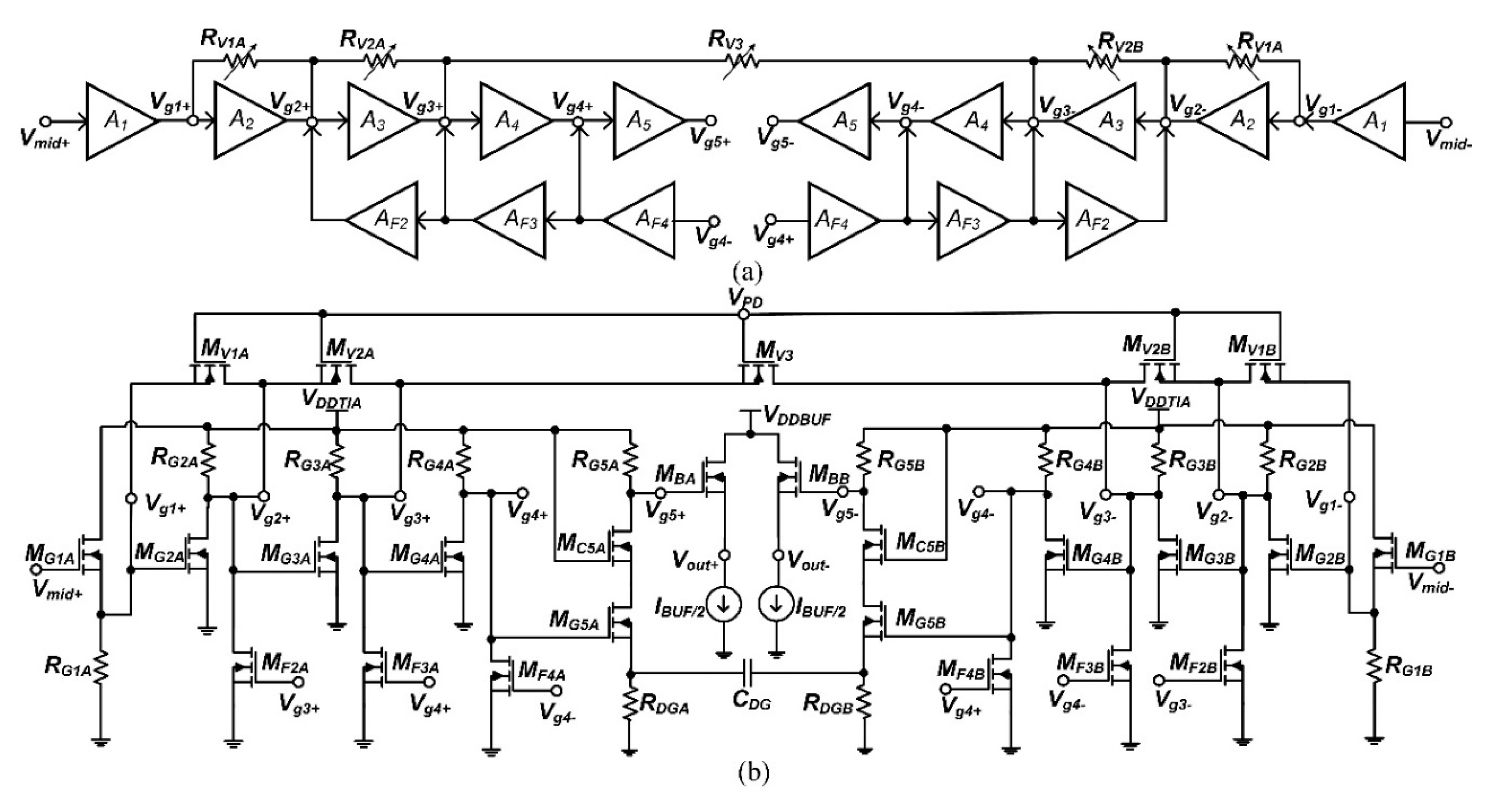
3.2. Proposed DVGTIA Gain Stage

Both DVGTIA designs 1 and 2 share the same gain stage design as in [7] as shown in Figure 5. There is a source-follower M G 1 A | 1 B followed by four CS amplifiers differential pairs M G 2 , 3 , 4 , 5 that give gains A G 2 , 3 , 4 , 5 , while three interleaving feedback transistor pairs M F 2 , 3 , 4 produce negative feedback gains A F 2 , 3 , 4 . The feedbacks introduce zeros at V g 2 , 3 , 4 , thus boosting bandwidth by gain peaking [6,7].
A unique advantage of the proposed DVGTIA gain stage is that it allows the same number of interleaving feedbacks as that of gain stages since the last interleaving feedbacks M F 4 A | 4 B can be from the opposite sides V g 4 and V g 4 + respectively [6,7]. A single gain varying DC bias V P D controls all gain varying transistors M V 1 , 2 , 3 across the CS amplifiers and lowers the gain at high input signal. This prevents non-linearity when the input signal strength increases which can cause signal distortion or clipping throughout the signal path. Thus, variable-gain increases the dynamic range of the TIA [5,7].
The gains at DC in the gain stage is listed in Table 2.
The poles and zeros can be calculated for the gain stage, with ω G 2 , 3 , 4 , 5 poles contributed by the gain transistors M G 2 , 3 , 4 , 5 and ω F 2 , 3 , 4 poles and zeros contributed by feedbacks M F 2 , 3 , 4 :
ω G 2 , 3 , 4 , 5 =   1 R G 2 , 3 , 4 , 5 C o , G 2 , 3 , 4 , 5
ω F 2 , 3 , 4 =   1 R G 2 , 3 , 4 C o , G 2 , 3 , 4
where C o , G 2 , 3 , 4 , 5 is the output parasitic capacitances at V g 2 , 3 , 4 , 5 at both positive and negative sides.
Voltage gain of the gain stage (with both sides being equal) is calculated as:
A g a i n = A G 2 A G 3 A G 4 A G 5 ( 1 + s ω F 2 , 3 , 4 ) ( 1 + s ω D 5 ) ( 1 + s ω G 2 , 3 , 4 ) ( 1 + s ω F 2 , 3 , 4.5 ) ( 1 + s ω D 5 ) A G 2 A G 3 A F 2 A G 3 A G 4 A F 3 + A G 4 A F 4
Hence, the differential gain equation of the entire circuit for DVGTIA designs 1 and 2 are:
Z T , D V G T I A 1 , d i f f = ( Z T i n 1 + Z T i n 1 ) × A g a i n
Z T , D V G T I A 2 , d i f f = ( Z T i n 2 + Z T i n 2 ) × A g a i n
After the DVGTIA gain stage, the buffer stage is a simple source-follower M B A | B B with the load being an NMOS current mirror current source I B U F / 2 of 2 mA on each side to match to 50 Ω.

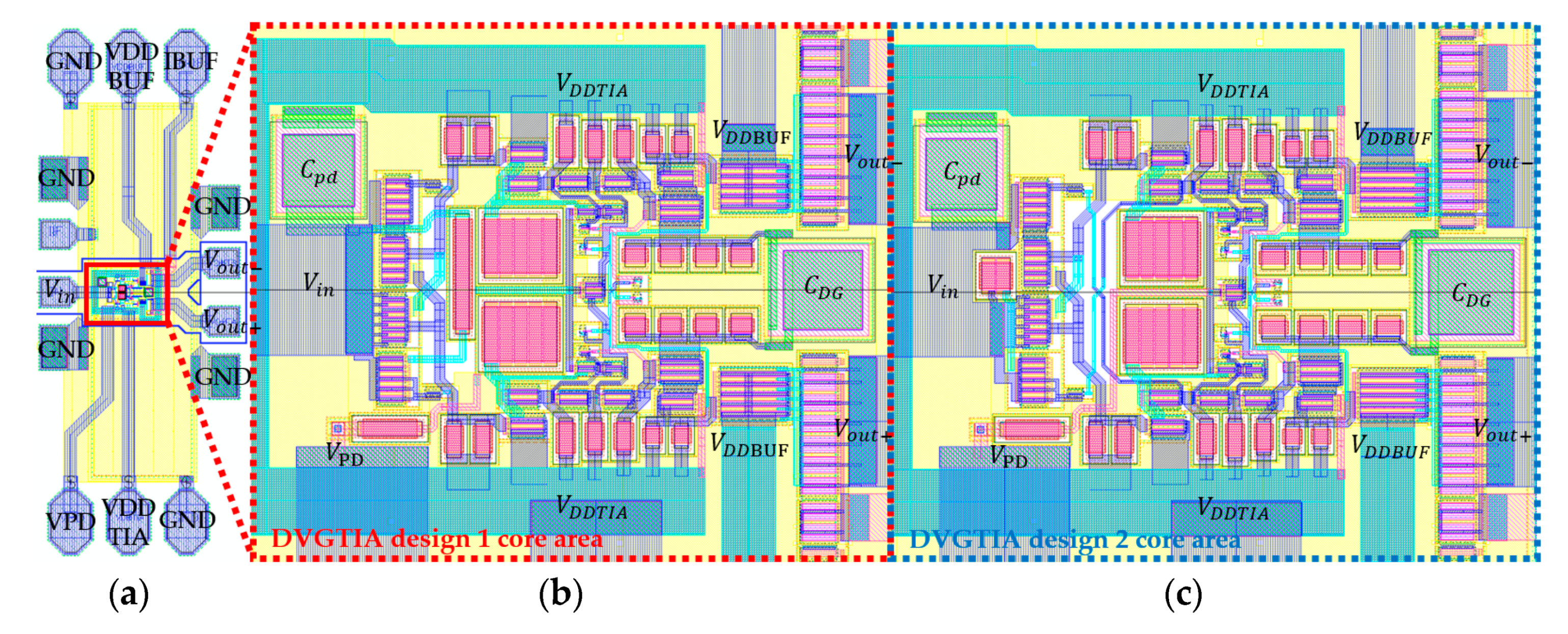
3.3. Layout and Die Microphotograph

The TIA layout is shown in Figure 6 and it has two three-pin DC pads at the top and bottom and two ground-signal-signal-ground (GSSG) input/output pads on the left/right respectively. The V D D is 1.8 V for both the core TIA and buffer while I B U F is 4 mA.   V P D is the voltage biasing for gain variation and varies from 1 V to 1.8 V. The 250 fF C p d load is included on-chip to show that the TIA designs can handle a real photodetector load. All schematic, layout and post-layout simulation results are done with the Cadence software design tool.
After the finalization of layouts of both DVGTIA designs, they are sent to Tower Semiconductor Ltd. (TowerJazz) foundry for manufacturing, with the die microphotographs of the actual taped-out chips shown in Figure 7.

3.4. Measurement Setup

The measurement setup is shown in Figure 8. The DC voltage and current biasing for the device under test (DUT) is provided by the Keysight B1500A Semiconductor Device Analyzer which is also able to measure current for V D D power supply. S-parameter and IP1dB analysis is done by the Keysight PNA-X N5247A Network Analyzer.
The measured DC currents for V D D T I A and V D D B U F are shown in Table 3:

4. Results and Discussion

4.1. Frequency Response from S-parameters

Both simulation and measurement results are presented in this paper for comparison. Measurement data in S-parameters can be converted to differential Z-parameter transimpedance gain through Equation (13) to plot Figure 9.
Z T , d i f f = Z 41 Z 21 =   2 S 41 × Z p o 1 Z p o 4 ( 1 S 11 ) ( 1 S 44 ) S 14 S 41   2 S 21 × Z p o 1 Z p o 2 ( 1 S 11 ) ( 1 S 22 ) S 14 S 21   Ω
where Z p o 1 ,   Z p o 2 ,   Z p o 4 are the impedances of ports 1, 2 and 4 in the measurement setup and are all 50 Ω, while port 3 is unused.   Z T , d i f f gain in Equation (13) can also be reported in dBΩ as in Figure 9.
As shown in Figure 9, the measured frequency response of both DVGTIA designs 1 and 2 are flat and stable across most of the bandwidth from 10 MHz to 10 GHz. The measured gains for when V P D = 1 V and 1.2 V are similar and some gain drop only occurs when it is increased to 1.4 V. Although gain peaking is within 1 dBΩ for simulation, however due to process variation for the tape-out chips, gain peaking becomes within 2 dBΩ for DVGTIA design 1 (except for V P D = 1.4 V) but above the limit for DVGTIA design 2. This could be corrected in a future design by having a variable peaking design that controls a zero to reduce the peaking due to process design kit (PDK) variation. The differences in frequency response between both designs are due to the different automatic feedbacks at V i n that cause different pole/zero pairs as mentioned in Section 3.1. In addition, the load of design 2 is slightly larger causing a slightly higher gain.
The maximum gain when V P D = 1 V is 60.6 and 62.8 dBΩ for DVGTIA designs 1 and 2 respectively, which reduces to a minimum gain of 24.5 and 27.8 dBΩ respectively when V p d = 1.8 V. Hence, the gain variations of DVGTIA designs 1 and 2 are 36.1 dBΩ and 35 dBΩ respectively. This gain variation helps to increase the TIA input dynamic range which will be explained in Section 4.2. The 3 dB bandwidth for DVGTIA design 1 is 6.42 GHz at V P D = 1 V, except when V P D = 1.4 V where the bandwidth is reduced to 5.03 GHz (3dB above gain at 85 MHz) before the large peaking, which can be ignored if V p d = 1.4 V is not used. Bandwidths for the other V p d biasings are larger than 6.42 GHz and thus there is no bandwidth loss during gain variation.
The simple source follower buffer M B A | B B and I B U F , after the gain stage as shown in Figure 5b has a gain drop of 2.7 dBΩ found in post-layout simulation. Hence, when buffer loss is de-embedded, the maximum gains for the chip of DVGTIA designs 1 and 2 are 63.3 dBΩ and 65.5 dBΩ respectively.
The 3 dB bandwidth for DVGTIA design 2 is 5.22 GHz at V p d = 1 V which is before the large peaking. If the peaking had been controlled, it could be higher at 7.36 GHz instead. The bandwidth is slightly reduced at V p d = 1.8 V to 5.11 GHz which is the lowest among all V p d biasings.

4.2. Input Referred 1dB Compression Point

The input 1 dB compression point (IP1dB) is the input power where the output 1 dB compression point (OP1dB) occurs, which is when the gain became compressed by 1 dB as compared to when the input power P i n is low. The IP1dB is a parameter to check the signal linearity of individual amplifiers and for the entire receiver module [16] and is plotted in Figure 10 for both DVGTIA designs.
The variable-gain DVGTIA designs in this paper increases the upper limit of the dynamic range which is determined by the IP1dB when the V P D = 1.8 V and gain is tuned to be the lowest. As shown in Figure 10, P i n is swept from −30 dBm to 0 dBm. The input 1dB compression point when V p d = 1 V is −27 dBm and −27.4 for DVGTIA designs 1 and 2 respectively, with the baseline P i n = −30 dBm used for comparison. The IP1dB increases when V p d = 1.8 V to −7.5 dBm (0.178 mW) and −7 dBm (0.2 mW) for DVGTIA designs 1 and 2 respectively. This proves that IP1dB increases significantly as V P D biasing is increased. The dynamic range for TIA is defined as the input current signal range that it is able to amplify without significant signal distortion at output. Thus, the upper limit of the input dynamic range in terms of current can be calculated from P i n of the IP1dB by taking the power formula [17]:
P i n =   I i n 2 Z i n  
where Z i n is found to be 19.5 Ω and 28.1 Ω for DVGTIA designs 1 and 2 respectively, in post-layout simulation. Hence, the dynamic range upper limit is calculated to be 3 mA and 2.7 mA respectively.

4.3. Noise

The lower limit of the dynamic range is determined by the noise level, since the noise of the TIA would distort the input signal if it is too small. The allowable signal-to-noise ratio (SNR) for TIA designs with a maximum bit error rate (BER) of 10 12 is 16.9 dB (≈49) [18]. The simulated output-referred noise voltage (ORNV) is shown in Figure 11.
Taking the ORNV in Figure 11 and the maximum gains at V P D = 1V in Figure 9, the input-referred noise current (IRNC) of DVGTIA designs 1 and 2 are calculated to be 10.3 p A / H z and 21.7 p A / H z at bandwidths 6.4 GHz and 5.2 GHz respectively. Hence by taking SNR = 49 and multiplying H z at bandwidth operation, the minimum input current needed is calculated as 40.4 µA and 76.8 µA for the lower limit of the input dynamic range of DVGTIA designs 1 and 2 respectively.
Sensitivity, which is defined as the minimum input signal S m i n required to produce an output signal greater than the required signal-to-noise ratio of both DVGTIA designs can also be calculated. The formula for sensitivity is [19]:
S m i n = ( S / N ) m i n × k × T o × B W × N F  
where ( S / N ) m i n is the signal-to-noise ratio, k is the Boltzmann constant, T o is the absolute temperature (300 K), BW is the bandwidth and NF is the noise figure.
The simulated noise figures of DVGTIA designs 1 and 2 are found to be 11.4 dB and 33.9 dB at bandwidths 6.4 GHz and 5.2 GHz respectively. By using (15), the sensitivity is calculated to be −47.5 dBm and −25.6 dBm for DVGTIA designs 1 and 2. As shown in Figure 11, the largest contributor of noise is the gain stages of the DVGTIA designs. The larger noise of the DVGTIA designs is due to three reasons. Firstly, there is the on-chip C p d , whereas other designs may have an off-chip or an ideal noiseless C p d in simulation to run together after obtaining the measurement results. Secondly, the designs have multiple stages with the second stage as a source follower being a significant problem. This is shown in Friis’ formula, which can be used to calculate the contribution of each stage in an amplifier to find the total noise factor [20]:
F t o t a l = F 1 + F 2 1 G 1 + F 3 1 G 1 G 2 + + F n 1 G 1 G 2 G n 1  
where F n is the noise factor of the n t h stage and G n is the gain of the n t h stage.
According to (16), each cascaded stage contributes noise divided by the gains of the previous stages. Since the gain of the source follower is lower than 1, it contributes to more overall noise F t o t a l . Thirdly, the cascaded common-source amplifiers in the gain stage are not differential stages with a single current source for both sides that can cancel the common-mode noise but separate common-sources amplifiers on both sides. This would thus increase the gain but prevent noise cancellation.

4.4. Eye Diagram

The measured eye diagrams of the DVGTIA designs 1 and 2 are shown in Figure 12. The input signal is a pseudorandom binary sequence (PRBS) at 5 Gb/s with V p p = 1 V. As seen in Figure 12, both eyes are open and clear, with eye heights of approximately 250 mV, eye widths of approximately 150 ps and jitter of less than 100 ps. This proves that the DVGTIA designs can function normally at the high data rate of 5 Gb/s even with an input signal of random sequence. The eye diagrams plotted are single-ended (A/+ side) during measurement using the R&S RTO 1044 oscilloscope.

4.5. Reliablity

The reliability of the DVGTIA designs can also be tested. In simulation, the temperature and C p d load can be varied to check if the TIA design still works as an amplifier and outputs a good frequency response. As shown in Figure 13a, DVGTIA design 1 still works well when the temperature is varied from −40 °C to 80 °C. In addition, when C p d increased from 0.25 pF–2 pF (800%), the bandwidth is reduced only from 6.39 GHz to 4.38 GHz (−31%). This shows that the design is able to withstand a large C p d load as the low Z i n is able to shield the C p d impact on the dominant pole. This is a big advantage for this design as a larger photodiode can be used to absorb more light to output a larger and more detectable current input for the TIA. However as shown in Figure 13b, DVGTIA design 2 encounters instability when temperature deviates too far from 27 °C and also when C p d is increased.

5. Discussion

5.1. Comparison of Theory and Simulation/Measurement Results

The theoretical equations of the gains for the gain stage (10) of the DVGTIA designs can be calculated and compared with the simulation/measurement results to check if they are accurate. The calculation for DVGTIA design 1 is shown in Table 4, but it is similar for design 2 as well. For DVGTIA design 1, the measured differential Z T , d i f f 1 at V O U T is 60.6 dBΩ as in Figure 9a. Using the simulated Z T , d i f f , i n p u t at V m i d and Z T , d i f f , g a i n at V g 5 for the gain stage in Figure 13a and the buffer stage gain drop of 2.7 dBΩ, the gain due to the gain stage is calculated to be 16.5 dBΩ (6.7 times gain).
There is a source follower stage M G 1 and R G 1 that is not accounted for in (10) which has been assumed to have a gain approximately equal to 1, but its gain is closer to 0.5 in reality, as well as including other losses. Hence, half of the gain 13.1 times is 6.5 times which is close to the simulation/measurement results calculated above.

5.2. Figure of Merit

F O M 1 = G a i n   ( Ω ) × B a n d w i d t h   ( G H z ) × C p d   ( p F )   C o r e   P o w e r   ( m W )  
F O M 2 = G a i n   ( Ω ) × B a n d w i d t h   ( G H z ) × C p d   ( p F ) × G a i n   R a n g e   ( d B Ω ) C o r e   P o w e r   ( m W )  
Two different figure of merits (FOMs) formulas are shown in (17) and (18) to compare with other recent variable-gain TIA works. F O M 1 consists of four different parameters including the gain, bandwidth and C p d load which are desired to be large as well as the core power which is desired to be small. All these parameters are key for determining the effectiveness of a TIA design. F O M 2 includes the gain range to include the advantage of having a wide gain-variation design.
As shown in Table 5 below, the DVGTIA designs have good F O M 2 values due to their large gain variation which is more than the other comparable designs.
Although designs in [21] and [24] also have high F O M 2 , they both only operate on a narrow bandwidth less than 1 GHz, in addition with [24] being a much smaller and more advanced process. The gain-bandwidth trade-off for this paper’s designs is acceptable for TIAs that function above 5 GHz. Although both have a slightly higher power consumption and noise due to the large number of CS stages in the gain stage, this allows the largest gain variation to be tuned among all designs and thus resulting in a wide input current dynamic range suitable for the range of current output from a real photodetector [7,10].

6. Conclusions

In conclusion, the authors presented two different inductorless differential variable gain transimpedance amplifier (DVGTIA) designs with a voltage-controlled variable-gain using Tower Jazz Semiconductor’s 0.18-µm SiGe BiCMOS process, while also being compatible with a pure-CMOS process. The designs are unique since they take a single-ended input to become a differential output while maintaining the low input impedance of a RGC configuration, as well as having a small additional automatic negative feedback to lower input impedance even further to compensate the large photodetector capacitive load, which is proven for DVGTIA design 1 in the reliability analysis. The gain stage is also able to provide a good gain while maintaining the bandwidth throughout due to its interleaving feedbacks and capacitive degeneration techniques.
The measurement results after chip tape-out is presented, with gain ranges of 24.5–60.6 dBΩ and 27.8–62.8 dBΩ and bandwidths of 6.42 GHz and 5.22 GHz for DVGTIA designs 1 and 2 respectively while having an on-chip capacitive load of 250 fF modelling a real photodetector. If buffer gain drop of 2.7 dBΩ is de-embedded, the maximum gains would be 63.3 dBΩ and 65.5 dBΩ respectively. By varying the biasing voltage, very wide gain ranges of 36.1 dBΩ and 35 dBΩ with no drop in the bandwidths achieved. This translates into giving wide input current dynamic ranges of 40.4 µA to 3 mA and 76.8 µA to 2.7 mA which fits the real photodetector’s current output.
Both DVGTIA designs also have an input referred noise current of 10.3 pA/ H z and 21.7 pA/ H z (simulation), core DC power consumption of 30.7 mW and 27.5 mW and compact core area of 100 µm × 85 µm. They both have the best figure of merit as defined in this paper with five key TIA parameters for designs above 5 GHz operation.

Author Contributions

S.B.S.L. contributed to the schematic design, layout, simulation in software and measurement results of the actual chip of the proposed circuit, as well as the writing of this paper. H.L. contributed to advice on the design process, tape-out compilation, measurement process and editing of this paper. J.-M.C. and X.Y. are the collaborators of this project while K.S.Y. is the overall project Principal Investigator. All authors have read and agreed to the published version of the manuscript.

Funding

This research was funded by the Singapore University of Technology and Design, grant award number ZJURP1600104.

Acknowledgments

The authors would like to acknowledge the Singapore University of Technology and Design (SUTD) for their support of this research and TowerJazz Semiconductor Ltd. for the process design kit.

Conflicts of Interest

The authors declare no conflict of interest.

References

  1. Karunatilaka, D.; Zafar, F.; Kalavally, V.; Parthiban, R. LED based indoor visible light communications: State of the art. IEEE Commun. Surv. Tutor. 2015, 17, 1649–1678. [Google Scholar] [CrossRef]
  2. Ergul, O.; Dinc, E.; Akan, O. Communicate to illuminate: State-of-the-art and research challenges for visible light communications. Phys. Commun. 2015, 17, 72–85. [Google Scholar] [CrossRef] [Green Version]
  3. Romanova, A.; Barzdenas, V. A Review of Modern CMOS Transimpedance Amplifiers for OTDR Applications. Electron. J. 2019, 8, 1073. [Google Scholar] [CrossRef] [Green Version]
  4. Samuel, L.B.S.; Sern, T.Y.; Kumar, T.B.; Yeo, K.S.; Li, Z.; Yu, X. An inductorless transimpedance amplifier design for 10 Gb/s optical communication using 0.18-μm CMOS. In Proceedings of the 15th International Symposium on Integrated Circuits (ISIC), Singapore, 12–14 December 2016. [Google Scholar]
  5. Samuel, L.B.S.; Sern, T.Y.; Kumar, T.B.; Yeo, K.S. An inductorless variable-gain transimpedance amplifier design for 4GHz optical communication using 0.18-μm CMOS. In Proceedings of the International Conference on Computer Networks and Communication Technology (CNCT 2016), Xiamen, China, 16–18 December 2016; Atlantis Press: Paris, France, 2016; Volume 54. [Google Scholar]
  6. Samuel, L.B.S.; Kumar, T.B.; Qiong, Z.; Yeo, K.S. An inductorless differential transimpedance amplifier design for 5 GHz optical communication using 0.18-µm CMOS. In Proceedings of the 14th IEEE International Conference on Solid-State and Integrated Circuit Technology (ICSICT), 2018, Qingdao, China, 31 October–3 November 2018. [Google Scholar]
  7. Lee, S.B.S.; Liu, H.; Yeo, K.S. An inductorless 6-GHz variable gain differential transimpedance amplifier in 0.18-μm SiGe BiCMOS. In Proceedings of the IEEE International Symposium on Circuits and Systems (ISCAS), 2019, Sapporo, Japan, 26–29 May 2019. [Google Scholar]
  8. Lee, S.B.S.; Liu, H.; Yu, X.; Chen, J.M.; Yeo, K.S. An inductorless 5-GHz differential dual regulated cross-cascode transimpedance amplifier using 40 nm CMOS. In Proceedings of the IEEE 13th International Conference on ASIC (ASICON) 2019, Chongqing, China, 29 October–1 November 2019. [Google Scholar]
  9. Royo, G.; Sanchez-Azqueta, C.; Aldea, C.; Celma, S.; Gimeno, C. CMOS transimpedance amplifier with controllable gain for RF overlay. In Proceedings of the 12th Conference on Ph.D. Research in Microelectronics and Electronics (PRIME) 2016, Lisbon, Portugal, 27–30 June 2016. [Google Scholar]
  10. Liu, H.; Zhu, X.; Boon, C.C.; Yi, X.; Kong, L. A 71 dB 150 µW variable-gain amplifier in 0.18 µm CMOS technology. IEEE Microw. Wirel. Compon. Lett. 2015, 25, 334–336. [Google Scholar] [CrossRef]
  11. Liu, H.; Zhu, X.; Boon, C.C.; He, X. Cell-Based variable-gain amplifiers with accurate dB-linear characteristic in 0.18 µm CMOS technology. IEEE J. Solid-State Circuits (JSSC) 2015, 50, 586–596. [Google Scholar] [CrossRef]
  12. Liu, H.; Boon, C.C.; He, X.; Zhu, X.; Yi, X.; Kong, L.; Heimlich, M.C. A wideband analog-controlled variable-gain amplifier with dB-linear characteristic for high-frequency applications. IEEE Trans. Microw. Theory Tech. 2016, 64, 533–540. [Google Scholar] [CrossRef]
  13. Kumar, T.B.; Ma, K.; Yeo, K.S. A 4 GHz 60 dB variable gain amplifier with tunable DC offset cancellation in 65 nm CMOS. IEEE Microw. Wirel. Compon. Lett. 2015, 25, 37–39. [Google Scholar] [CrossRef]
  14. Taghavi, M.H.; Belostotski, L.; Haslett, J.W. A CMOS low-power cross-coupled immittance-converter transimpedance amplifier. IEEE Microw. Wirel. Compon. Lett. 2015, 25, 403–405. [Google Scholar] [CrossRef]
  15. Chen, D.D.; Yeo, K.S.; Shi, X.; Manh, A.D.; Chirn, C.B.; Wei, M.L. Cross-coupled current conveyor based CMOS transimpedance amplifier for broadband data transmission. IEEE Trans. Very Large Scale Integr. (VLSI) Syst. 2013, 21, 1516–1525. [Google Scholar] [CrossRef]
  16. Eissa, M.H.; Malignaggi, A.; Wang, R.; Elkhouly, M.; Schmalz, K.; Ulusoy, A.C.; Kissinger, D. Wideband 240-GHz transmitter and receiver in BiCMOS technology with 25-Gbit/s data rate. IEEE J. Solid-State Circuits (JSSC) 2018, 53, 2532–2542. [Google Scholar] [CrossRef]
  17. ElectronicsTutorials.ws, Power Triangle and Power Factor. Available online: https://www.electronics-tutorials.ws/accircuits/power-triangle.html (accessed on 3 June 2020).
  18. Sackinger, E. Analysis and Design of Transimpedance Amplifiers for Optical Receivers; John Wiley & Sons, Inc.: Hoboken, NJ, USA, 2017. [Google Scholar]
  19. University of Hawaii Department of Physics and Astronomy, Receiver Sensitivity/Noise. Available online: https://www.phys.hawaii.edu/~anita/new/papers/militaryHandbook/rcvr_sen.pdf (accessed on 3 June 2020).
  20. McCorkle, J. Microwaves101.com, Noise Figure One and Two Friss and IEEE. Available online: https://www.microwaves101.com/encyclopedias/noise-figure-one-and-two-friis-and-ieee (accessed on 3 June 2020).
  21. Ngo, T.H.; Kim, C.H.; Kwon, Y.J.; Ko, J.S.; Kim, D.-B.; Park, H.-H. Wideband receiver for a three-dimensional ranging LADAR system. IEEE Trans. Circuits Syst. I Regul. Pap. 2013, 60, 448–456. [Google Scholar] [CrossRef]
  22. Schoeniger, D.; Henker, R.; Ellinger, F. A high-speed energy-efficient inductor-less transimpedance amplifier with adjustable gain for optical chip-to-chip communication. In Proceedings of the SBMO/IEEE MTT-S International Microwave and Optoelectronics Conference (IMOC) 2015, Porto de Galinhas, Brazil, 3–6 November 2015. [Google Scholar]
  23. Chen, R.Y.; Yang, Z.Y. CMOS transimpedance amplifier for gigabit-per-second optical wireless communications. IEEE Trans. Circuits Syst. Ii Exp. Briefs 2016, 63, 418–422. [Google Scholar] [CrossRef]
  24. Royo, G.; Martinez-Perez, A.D.; Aldea, C.; Celma, S. A Highly Linear Low-Noise Transimpedance Amplifier for Indoor Fiber-Wireless Remote Antenna Units. Electron. J. 2019, 8, 437. [Google Scholar] [CrossRef] [Green Version]
Figure 1. Standard RGC TIA design with additional cascode transistor M 3 [3,4,5,6,7].
Electronics 09 01058 g001
Figure 2. Cross-coupling single-ended TIA design with RGC input design as in [14].
Electronics 09 01058 g002
Figure 3. Cross-coupling differential TIA design with simple CG input design as in [15].
Electronics 09 01058 g003
Figure 4. (a) Simplified and (b) transistor-level schematic of the proposed DVGTIA input stage design 1 and (b) design 2.
Electronics 09 01058 g004
Figure 5. (a) Simplified and (b) transistor-level schematic of the proposed DVGTIA gain stage for both designs 1 and 2 together with the source follower buffer.
Electronics 09 01058 g005
Figure 6. (a) TIA layout design with pads and (b) core area only of DVGTIA design 1 and (c) DVGTIA design 2 (both core area: 100 µm × 85 µm, total area with pads: 350 µm × 910 µm).
Electronics 09 01058 g006
Figure 7. (a) Die microphotographs of the overall DVGTIA design 1 and 2 layouts, (b) core circuit of DVGTIA design 1 and (c) core circuit of DVGTIA design 2.
Electronics 09 01058 g007
Figure 8. Measurement setup for S-parameters and input referred 1 dB compression point.
Electronics 09 01058 g008
Figure 9. (a) Post-layout simulation and measured frequency response of the DVGTIA design 1 and (b) DVGTIA design 2 with varying V P D at 1 V, 1.4 V, 1.6 V and 1.8 V.
Electronics 09 01058 g009
Figure 10. (a) Post-layout simulation and measured IP1dB compression curve of the DVGTIA design 1 and (b) DVGTIA design 2 with V P D at 1 V, 1.4 V, 1.6 V and 1.8 V.
Electronics 09 01058 g010
Figure 11. (a) Post-layout simulation in Cadence of the output referred noise voltage at TIA bandwidth as well as noise contribution at V m i d (output of input stage) and V g 5 (output of gain stage) of DVGTIA design 1 and (b) DVGTIA design 2 with V P D at 1 V, 1.4 V, 1.6 V and 1.8 V.
Electronics 09 01058 g011
Figure 12. (a) Measured eye diagrams with 5 Gb/s PRBS input signal of DVGTIA design 1 and (b) DVGTIA design 2.
Electronics 09 01058 g012
Figure 13. (a) Reliability testing in post-layout simulation by increasing C p d and varying temperature as well as differential gain across V m i d and V g 5 for DVGTIA design 1 and (b) DVGTIA design 2.
Electronics 09 01058 g013
Table 1. Table of gain functions at DC in DVGTIA input stage.
Gain * V o / V i Transfer FunctionGain * V o / V i Transfer Function
A C S , M 1 A V m i d / V m i d + g M 1 A R 1 A A C S , M 3 A V i n / V m i d + g M 3 A R 1 A
A C S , M 1 B V m i d + / V m i d g M 1 B R 1 B A C S , M 3 B V i b / V m i d g M 3 B R 1 B
A C G , M 1 A V m i d + / V i n ≈1 A C S , M 4 A V i n / V g 2 g M 4 B R G 2 B
A C G , M 1 B V m i d / V i b ≈1 A C S , M 4 B V i b / V g 2 + g M 4 A R G 2 A
A C S , M 2 B V i b / V i n g M 1 B R 1 B
* Care must be taken in defining the gains A; in this paper, the negative sign of CS amplifier gain is inside A.
Table 2. Table of gain functions in DVGTIA gain stage.
Gain * V o / V i Transfer FunctionGain * V o / V i Transfer Function
A G 2 , 3 , 4 , 5 V g 2 , 3 , 4 , 5 / V g 1 , 2 , 3 , 4 g M G 2 , 3 , 4 , 5 R G 2 , 3 , 4 , 5 A F 2 , 3 , 4 V g 2 , 3 , 4 / V g 3.4.4 # g M F 2 , 3 , 4 R G 2 , 3 , 4
* Care must be taken in defining the gains A; in this paper, the negative sign of CS amplifier gain is inside A. # Note that two of the feedbacks are from the same V g 4 + and V g 4 nodes, just across to different stages.
Table 3. Measured DC currents for voltage power supply.
I D C   for   V D D T I A   ( mA ) Core Power (mW) I D C   for   V D D B U F   ( mA ) Total Power (mW)
DVGTIA design 117.0830.710.7350.1
DVGTIA design 215.2527.511.4648.1
Table 4. Simulation gain calculations for DVGTIA design 1.
GainEquationSim ValueGainEquationSim Value
A G 2 g M G 2 R G 2 −3.51 A F 2 g M F 2 R G 2 −0.23
A G 3 g M G 3 R G 3 −2.61 A F 3 g M F 3 R G 3 −0.05
A G 4 g M G 4 R G 4 −3.20 A F 4 g M F 4 R G 4 −0.14
A G 5 g M G 5 R G 5 −1.77Equation (10) gain13.1 times
Table 5. Table of comparison with other recent works.
ReferenceUnit[9] a[21] b[22][23][24]This Work
Technologynm180 CMOS130 CMOS130 BiCMOS180 CMOS65 CMOS180 BiCMOS
Design1  Design2
V D D V1.833.31.81.21.8
C p d pF0.920.020.250.450.25
Maximum gain dBΩ667865.169.37660.6 c62.8 c
Ω1995794317932917631010721380
Minimum gaindBΩ484856.755.86024.527.8
Ω251251684617100016.824.5
Gain rangedBΩ18308.413.51636.135
BandwidthGHz1.50.646.810.36.425.22
Core powermW2711421.26630.727.5
Core areamm2N.A.0.2830.00780.00750.0150.0085
Input-referred noise currentpA/√Hz6 d5.64.34 d9.332 d10.3 d21.7 d
F O M 1 Equationn (17)10089121221425665
F O M 2 Equationn (18)17962676971641227220222293
a This paper presents simulation results while others present measurement results; b core area is not known and it has high power consumption; c if gain drop of 2.7 dBΩ of buffer is de-embedded, gains would be 63.3 dBΩ and 65.5 dBΩ respectively; d simulation results presented for the input-referred noise current.

