Abstract
This work presents a single-stage, inverter-based, pseudo-differential amplifier that can work with ultra-low supply voltages. A novel common-mode stabilization loop allows proper differential operations, without impacting over the output differential performance. Electrical simulations show the effectiveness of this amplifier for supply voltages in the range of 0.3–0.5 V. In particular, a dc voltage gain of 25.16 dB, a gain-bandwidth product of 131.9 kHz with a capacitive load of 10 pF, and a static current consumption of only 557 nA are estimated at VDD = 0.5 V. Moreover, the circuit behavior with respect to process and temperature variations was verified. Finally, the proposed amplifier is employed in a switched-capacitor integrator and in a sample-and-hold circuit to prove its functionality in case-study applications.
1. Introduction
In recent years, the demand for circuits capable of working with very low supply voltages has increased. There are two main reasons: The first one is the continuous scaling of the supply voltage, which has marked the evolution of CMOS technologies, originating mainly from reliability issues of gate dielectrics and power dissipation limits at the maximum switching frequency. The second reason is an increasing interest in energy harvesting (or scavenging) devices, which are capable of providing very low supply voltages. Examples of circuits powered by that kind of devices are Wireless Sensor Networks (WSNs) [1] and wearable/implantable biomedical devices; some of the latter may potentially take advantage of biofuel cells, which can typically provide a supply voltage that does not exceed a few hundred millivolts [2]. Values such as these are usually close to the threshold voltage of regular MOSFETs: The use of particular sizing and topologies becomes mandatory in ultra-low voltage (ULV) design.
A very popular approach to ULV design is the use of inverter-like amplifiers [3]. In these particular architectures, each amplifier is substituted by a CMOS inverter, depicted in Figure 1a, which presents several benefits: compact layout, rail-to-rail output range, and good performance in terms of trade-off between speed, noise, and power consumption.
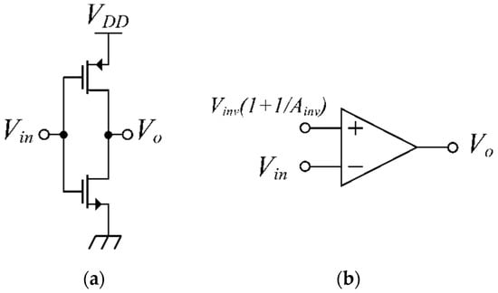
Figure 1.
(a) Standard CMOS inverter and (b) its equivalent differential amplifier.
Unfortunately, this type of circuit, when used as an amplifier, presents some drawbacks, such as: (i) strong dependence from Process-Voltage-Temperature (PVT) variations, (ii) lack of a physical non-inverting input, and (iii) low dc gain. A typical approach to overcome the low dc gain issue is to use the cascade of two or more gain stages equal to the one in Figure 1a, realizing a multistage amplifier. This kind of amplifier is almost mandatory if employed with resistive loads (as in resistive feedback configurations), being able to maintain a sufficiently high voltage gain. Unfortunately, with multiple gain stages, we need at least one compensation network to avoid instability, as well as more area and power consumption [4].
These problems are mitigated if a pure capacitive load (actual load plus feedback network) is applied, as in switched-capacitor (SC) circuits, where inverter-like amplifiers are being proposed as a replacement of more complex operational amplifier topologies. This is possible because, despite the absence of a non-inverting input, in most SC circuits the operational amplifier non-inverting terminal is grounded, or, equivalently, fixed to a constant voltage to meet input common-mode (CM) range requirements. The relatively small dc gain of inverter-like amplifiers can be overcome by using SC architectures capable of boosting the overall dc gain to the square [5] or even the cube (using two inverter stages) [6] of the original inverter gain. Considering this fact, as already stated, the ideal application of this kind of amplifiers lies just in SC circuits, such as discrete-time integrators, which are the main building blocks of state-variable filters and ΔΣ modulators [7].
Fully differential (FD) topologies are widely used in ULV systems. These architectures have several intrinsic benefits, such as: (i) strong rejection of CM interferences, (ii) larger output range, and (iii) improved linearity. To make these topologies working correctly, a proper system for the stabilization of the output CM voltage is necessary [8].
In this work, we present a pseudo-differential, single-stage, inverter-based amplifier for ULV applications with a novel common-mode stabilization loop (CMSL). The proposed circuit has been designed with the UMC 0.18 μm CMOS process and its effectiveness has been verified by means of electrical simulations. The rest of this paper is organized as follows. Section 2 introduces inverter-like amplifiers and describes the proposed architecture; in Section 3, the results of detailed electrical simulations are presented and compared with the well-known Nauta transconductor. Finally, examples of application of the proposed amplifier in standard SC circuits are illustrated in Section 4.
2. Proposed Pseudo-Differential Inverter-Based Amplifier
2.1. The CMOS Inverter Used as an Amplifier
As we can see in Figure 1, a simple inverter is equivalent to a differential amplifier with the non-inverting input permanently connected to the constant voltage Vinv (1 + 1/Ainv). The voltage Vinv represents the inverter switching voltage, i.e., the input value which produces Vout = Vin = Vinv; Ainv is the magnitude of the amplifier gain. In the equivalent circuit shown in Figure 1b, if Ainv is large enough, we can consider that the non-inverting input is fixed to Vinv. A very helpful characteristic of this topology in ULV applications is the capability of working with supply voltages lower than the sum of the nMOS and pMOS threshold voltages. This can be accomplished by making the transistors operate in subthreshold region.
Figure 2 shows the small-signal equivalent circuit of the inverter. With simple calculations we may find that its frequency response is equal to:
with:
where gm,n and gm,p are the transconductances of the nMOS and pMOS, respectively, rd,n and rd,p their output resistances, whereas CX, CY, and CZ are the combination of their parasitic capacitances (in CZ, a load capacitance CL is also taken into account). In a closed-loop configuration, the frequency response is mainly determined by the gain-bandwidth product (GBW), which can be easily found from Equation (1): It is approximately equal to Gm/2π(CY + CZ). Since in many SC circuits CL is the biggest capacitance, the GBW is much lower than the frequency of the zero, which from Equation (1) turns out to be Gm/2πCY. Both singularities are proportional to Gm, which, in turn, is proportional to the inverter bias current.
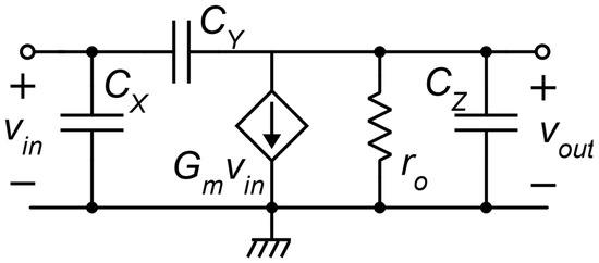
Figure 2.
Small-signal equivalent circuit of the inverter-like amplifier.
2.2. Fully Differential, Inverter-Based Amplifiers: Output Common-Mode Stabilization
In Figure 3a, a pseudo-differential, inverter-based amplifier is depicted together with a generic block (in grey lines) implementing a CMSL. In the absence of a CMSL, the CM to CM gain Acc is equal to the differential-mode (DM) to DM gain Add, which should be made large. As a result, even in the presence of small input CM variations, the output CM may drift as much as to impair the available differential output range. To overcome this problem and make the amplifier usable for SC applications, it is generally sufficient to reduce Acc to values close to one. Therefore, the aim of the CMSL is just to reduce Acc.
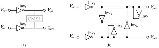
Figure 3.
(a) Pseudo-differential, inverter-based amplifier with CMSL circuit drawn in grey lines and (b) CMSL implementation proposed by Nauta in [9].
Several examples of pseudo-differential, inverter-based amplifiers with different circuits for the stabilization of the CM output voltage have been presented in the literature. One of the most popular is the Nauta transconductor [9], depicted in Figure 3b. In this circuit, the main differential path is formed by Inv1 and Inv2, while the CMSL is implemented by Inv3–6. The purpose of the Inv3–6 network is to act as a low resistive load for CM variations and as a high resistive load for DM ones. A well-known issue [10] of this circuit is the degradation of the differential output range due to the DM output resistance lowering, which starts at relatively small output voltages. The presence of a large output DM unbalances the transconductances of inverters pairs Inv3–4 and Inv5–6, disrupting the compensation mechanism that boosts the output resistance for small signals.
An alternative solution for the CM stabilization is presented in [11] in two different topologies: feedback and feedforward fashion. Both techniques present some limitations: The feedback one suffers from the degradation of the amplifier input impedance due to the presence of a resistance rd directly connected to the amplifier input terminals. On the other hand, the feedforward stabilization circuit is based on the matching properties of different inverters and could be not very robust against PVT variations.
2.3. The Proposed Inverter-Based Fully Differential Amplifier
Figure 4 shows the proposed pseudo-differential, inverter-based amplifier. The two main inverters (Inv1 and Inv2) process the differential input signal, while the other seven inverters (Inv3–Inv9) implement the CMSL. Obviously, for symmetry reasons, Inv1 is nominally identical to Inv2, Inv3 to Inv4, and Inv5 to Inv6. Inverters Inv3 and Inv4, loaded by unity-gain-connected Inv8, extract a signal proportional to the output CM voltage. This signal is inverted by Inv7, which is loaded by Inv9. Finally, Inv7 output signal (Vy) drives Inv5 and Inv6, which inject CM currents into the output nodes, closing the loop. Notice that at least in the case of perfect matching between Inv5 and Inv6, the proposed CMSL action will affect only the output signal CM components, so that degradation of Add does not occur. In terms of small signals, the symmetry between Inv3 and Inv4 makes Vx insensitive to the output DM voltage. On the other hand, large output differential voltages may affect Vx, due to the non-linear behavior of Inv3 and Inv4. This affects CMSL operation, causing the output CM to depend on the output DM. Nevertheless, the action of Inv5 and Inv6 is still symmetrical and the output DM voltage is not significantly altered. As a result, the proposed CMSL does not introduce significant degradation of the Add gain and of the DM range, with exception of the unavoidable reduction of the amplifier output DM resistance due to Inv5 and Inv6 output resistances. This effect can be made small by proper sizing of Inv5–6 MOSFETs: Choosing a higher channel length and/or a lower aspect ratio compared to Inv1–2. The latter choice was adopted as described later in this section.
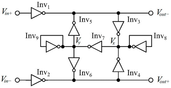
Figure 4.
Schematic view of the proposed single-stage, pseudo-differential, inverter-based amplifier.
By these considerations, the small-signal Add gain is simply given by:
where rok, Gmk indicates inverter Invk output resistance and its equivalent Gm, respectively.
As far as the response to CM input signals is concerned, the circuit of Figure 5 can be used. With simple calculations, it is possible to express the CM gain Acc as:
where ACMSL is the loop gain of the CM stabilization circuit, given by:
where we neglected the output inverter resistance that fall in parallel to the 1/Gm resistance of unity-gain-connected Inv8 and Inv9 and we used the above-mentioned symmetries, Gm1 = Gm2, ro1 = ro2 and ro5 = ro6. The target is making ACMSL larger than Add, so that Acc, given by Equation (4), becomes smaller than one. We start by saying that Inv5–6 strength (i.e., output current capability) cannot be much smaller than Inv1–2 one, otherwise the former cannot counteract Inv1–2 CM output for large signals. We chose to make Inv5 MOSFET aspect ratios just half of Inv1 ones. This halved the quiescent current of Inv5 with respect to Inv1 one, mitigating the power consumption overhead due to the CMSL and increasing ro5, with benefits in terms of DM mode gain. Then we chose to make Gm9 = Gm7 and Gm3 = 4Gm8. With these choices ACMSL = 4Add and Acc = 1/5, which is considerably smaller than 1, as required.
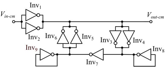
Figure 5.
Equivalent circuit for common-mode analysis.
2.4. Stability of the CMSL
Considering that in the proposed CMSL circuit there is a path formed by the three inverters cascaded Inv3,7,5 (i.e., a ring oscillator), it is important to study its stability. Inv8 presence partially mitigates this issue, but the high voltage gain provided by the cascade of Inv5 and Inv7 could still make the CMSL sizing quite difficult. For this reason, Inv9 was inserted to reduce the CMSL gain, analogously to Inv8. Moreover, thanks to its low resistance, it moves the pole associated with the impedance at node Vy to higher frequencies. Both these features increase stability but, on the other hand, reduce the effectiveness of the CMSL by lowering the Acc value. Notice that standard approaches for three-stage feedback loop stabilization, such as nested Miller compensation, are hindered by the presence of only inverting stages. Furthermore, adding capacitors across Inv3/Inv4 and/or across Inv5/Inv6 would increase the capacitive load of Inv1/Inv2 and degrade the DM frequency response of the amplifier.
2.5. Sizing of the Demonstrator
A FD amplifier based on the proposed topology was designed using the UMC 0.18 μm CMOS process. In Table 1 the size of every transistor in the amplifier is reported. For all the inverters we chose the minimum length allowed by the process (180 nm) to maximize the GBW. This choice decreases the differential gain but, as previously mentioned, this problem can be mitigated by using the amplifier in topologies with low sensitivity to the effect of finite gain. [5,6]. The various inverters differ for the widths of both n and p devices. In this way, we set the Gm ratios mentioned in Section 2.3. Figure 6 shows a preliminary layout of the proposed FD inverter-based amplifier: Multi-finger arrangement has been preferred to obtain a compact area and a good aspect ratio of the whole layout. The total amplifier size is 20 μm × 40 μm.

Table 1.
MOSFET dimensions of the amplifier inverters.
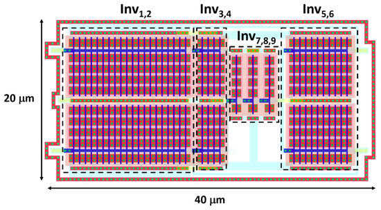
Figure 6.
Preliminary layout of the proposed amplifier; the dashed boxes include the area of the inverters, grouped as in Table 1. The cell is included into a ring of substrate contacts to reduce substrate noise.
3. Results and Discussion
The complete amplifier was simulated with the Cadence SpectreTM electrical simulator to test its dc performance, its frequency response, and the effectiveness of the proposed CMSL. All simulations were performed with a supply voltage VDD of 0.5 V and a load capacitance CL = 10 pF, unless otherwise specified. The proposed amplifier behavior was then compared with the one of the Nauta transconductor, which was sized as suggested in [10]; the sizing is visible in Table 2, with Figure 3b as a reference.
Table 2.
MOSFET dimensions of the Nauta transconductor inverters.
First, the frequency response of the two inverter-based amplifiers with an input CM voltage equal to VDD/2 was simulated. Figure 7 shows the simulation results of our circuit (solid line with triangle symbols) compared with the Nauta transconductor (dashed line with circle symbols). We can see that the proposed amplifier has a differential gain equal to 25.2 dB and it is about 2.5 dB higher than Nauta’s circuit, while the GBWs are similar and fall around 132 kHz. The phase margin PM of the proposed amplifier is 86°, while the Nauta transconductor one is 87°.
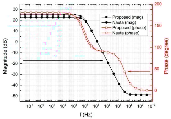
Figure 7.
Comparison between the magnitude and phase frequency responses of the proposed amplifier and of the Nauta transconductor.
Subsequently, a differential input was applied with the purpose of detecting the output linear range, again with an input CM equal to VDD/2. The significantly wider output linear range of our amplifier with respect to the Nauta transconductor is clear in Figure 8. To quantify this difference, we considered to be “linear range” the region of differential output voltage where the small-signal gain drop is less than 30% of the maximum value. By this definition, the output linearity range of the Nauta transconductor is around 110 mV, while our circuit reaches 586 mV.
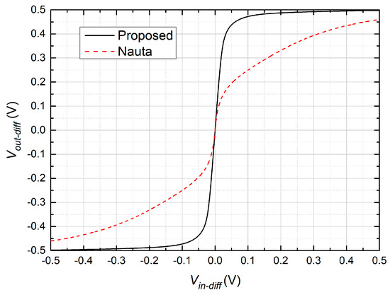
Figure 8.
Comparison of the differential input-output dc characteristics of the proposed amplifier and of the Nauta transconductor.
Using the stability analysis tool provided by the Spectre™ simulator, it was possible to also evaluate the loop gain and phase of the CM stabilization loop, here depicted in Figure 9. The actual stability of the CMSL is confirmed by the phase margin (PMCMSL) and the gain margin (GMCMSL), which turned out to be 51° and 14.16 dB, respectively.
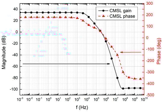
Figure 9.
Loop gain and loop phase Bode plots of the CMSL.
To further verify the correct behavior of our common-mode stabilization loop, the input CM was swept from 0 to VDD: The output CM is plotted in Figure 10. The proposed CMSL, compared to Nauta’s solution, provides a better attenuation of the output CM variations in the CM input range from about 70 mV to 430 mV; the slope around the mid-point is −0.92 for Nauta’s solution, while it is 3 times lower for ours.
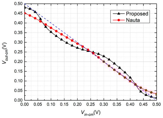
Figure 10.
Comparison between the common-mode input-output dc characteristics of the proposed amplifier and of the Nauta transconductor (the dotted curve is a unitary slope line).
The total current consumption (Is) is 558 nA, resulting in a dissipated power of 279 nW. It is possible to evaluate the efficiency of the bandwidth vs. power consumption trade-off by using the following Figure Of Merit (FOM) [10]:
which, for the proposed amplifier, turned out to be 237 V−1.
3.1. Temperature and Corner Variations
With ultra-low supply voltages, circuits are more prone to suffer from PVT variations. Therefore, we verified the robustness of our proposed amplifier by means of temperature sweep and corner analysis. Concerning supply voltage variations, the PSRR has been estimated by means of ac simulations performed on the amplifier closed in unity-gain configuration (input port shorted to the output one). The average PSRR low-frequency (1 Hz) value, resulting from 100 Monte Carlo runs, was 76.8 dB.
The variations of some of its most important parameters with respect to the temperature are more significant: We reported them in Table 3. We can notice the obvious, strong dependence of the power dissipated PD, and the GBW has the same trend as well. PMCMSL, instead, is practically constant over the whole tested range and so the loop remains stable for all temperatures. Globally, considering the inverter-based architecture and the ultra-low supply voltage, our circuit performs well for most of the temperatures.
Table 3.
Amplifier parameter variations versus temperature.
Corner analysis was also conducted. The amplifier proved again its robustness: We may report just a few minor flaws, which are a power consumption of 1.22 µW in the corner FF (Fast-nMOS, Fast-pMOS) and a GBW of 27 kHz in the corner SS (Slow-nMOS, Slow-pMOS). However, it has to be highlighted that in the first case, the GBW increased to 559 kHz, while in the latter case there was a reduction of the power dissipated to only 60 nW.
3.2. Simulations at 0.3 V Supply Voltage
All the previous simulations were repeated with a supply voltage of 0.3 V, to assess correct operation for ULV circuits and characterize performance degradation due to the reduced supply voltage. A summary of performances is provided in Table 4. The most important effect caused by the Vdd transition from 0.5 V to 0.3 V is a more than ten-fold reduction in the bias current of all inverters, due to the subthreshold exponential dependence of the drain current on the gate-source voltage. The consequence is a proportional degradation of the GBW, due to Gm1 and Gm2 reduction. Fortunately, all Gm’s vary in the same way, so that the relationships between the singularities of the CMSL are not seriously altered. This is proven by the phase margin of the loop that is even larger at 0.3 V (58 degrees). The Add reduction observed at Vdd = 0.3 V is less than 3 dB, while the CM gain Acc is lower than one for a quasi rail-to-rail input CM range. These figures confirm that the proposed amplifier can be used even at such extremely low voltages with only a few nanowatt of power consumption, when very slow-varying signals must be processed.
Table 4.
Comparison with other works.
3.3. Comparison with the State of the Art
In Table 4 a comparison between the proposed work and other inverter-based amplifiers in the literature is presented. All works were realized in a 0.18 μm technology. It is worth mentioning that the low dc gain of our prototype is due to the single-stage topology and the minimum channel lengths, introduced to maximize the trade-off between power consumption and bandwidth. The only other single stage shown in Table 3 takes advantage of longer channel lengths, body biasing and series–parallel MOSFET connections to increase the dc gain. Notice that the parameter PM in Table 3 is not the CMSL phase margin PMCMSL; instead, it represents the phase margin of the whole pseudo-differential amplifier. The CMSL phase margin has not been included in Table 4, since the papers used for comparison do not report on this datum.
4. Case Studies: Application of the Proposed Amplifier to SC Circuits
To show how the proposed circuit performs in an actual circuit, we analyzed its behavior when employed in a SC integrator and in a SC Sample-and-Hold (S/H) circuit. The supply voltage was set to 500 mV in both cases.
4.1. SC Integrator
As for the integrator, we chose the standard, strays-insensitive topology [13] shown in Figure 11.
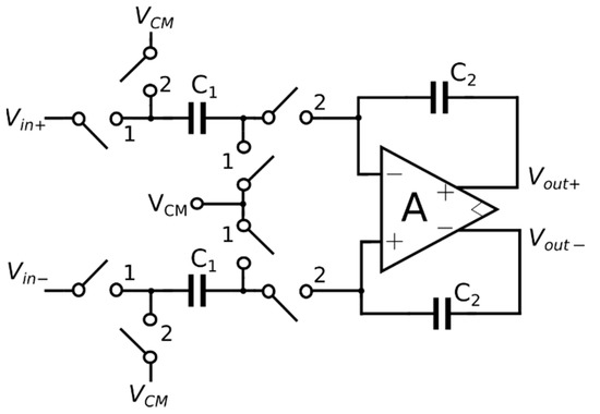
Figure 11.
Standard topology of a fully differential, SC integrator [13].
Once again, we compared our amplifier with the Nauta transconductor. The FD amplifier A was then implemented first with the circuit of Figure 4 and then with the one of Figure 3b; in addition, we adopted ideal switches in order to highlight only the differences between the two amplifier topologies and avoid additional non-idealities. The design of proper switches capable of working at very low supply voltages may be very challenging, typically requiring techniques of bootstrapping [14] and clock boosting [15], which here will not be discussed. The two capacitors C1 and C2 were set equal to 1 pF. Voltage VCM was set to half the supply. Figure 10 shows the DM and CM outputs of the integrator in both cases, when the input is a square wave with a differential amplitude of 100 mV and a CM equal to VCM. The clock signal driving the switches had a frequency of 10 kHz. The capacitive load, not shown in Figure 11 for the sake of simplicity, was 10 pF. The resulting staircase waveforms visible in Figure 12 prove that the proposed circuit introduces much less compression of the output signal than the integrator based on the Nauta transconductor. A progressive compression of the steps is also visible in the case of the proposed amplifier, but it is mainly due to the small dc gain, which make the output voltage tend to a finite value when a constant input is applied. We may also notice that the output CM is well stabilized for both circuits, with a maximum excursion of just a few mV. In this respect, the Nauta’s topology provides a slightly better stabilization.
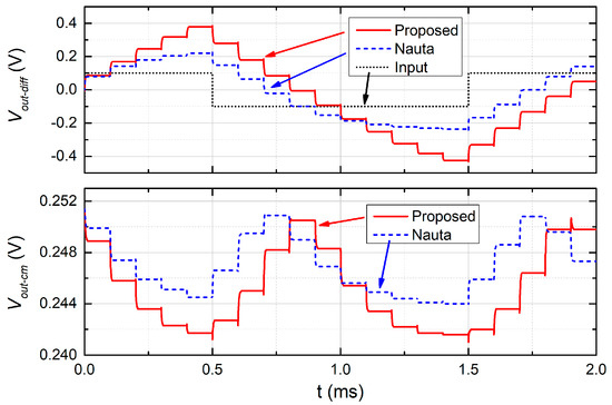
Figure 12.
Differential-(top) and common-mode (bottom) outputs of the SC integrator of Figure 9, implemented using the proposed amplifier (red solid line) and the Nauta transconductor (blue dashed line). The input signal is a rectangular waveform (pointed line in the upper plot).
4.2. S/H Circuit
For the S/H circuit, we chose the well-known flip-around topology [16] shown in Figure 13, which was already employed in sub-1 V applications [17]: In this way, we characterized the amplifier linearity performance in terms of harmonic distortion.
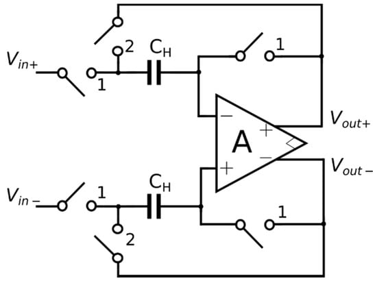
Figure 13.
Standard topology of a fully differential, SC S/H circuit [16].
As in the integrator case study, we used ideal switches to avoid non-idealities not related to the amplifiers and the capacitive loads were set to 10 pF. The clock frequency was set to 10 kHz, while the capacitors CH were chosen equal to 1 pF. An input signal, with sinusoidal differential mode and common-mode voltage fixed to 250 mV, was fed to the S/H circuit. The frequency of the input stimulus was 500 Hz, while its amplitude was swept from 50 to 500 mV. Simulations were performed using the S/H in Figure 13 comparing the performance of the proposed amplifier and the Nauta transconductor. The Total Harmonic Distortion (THD) was evaluated by means of the Discrete Fourier Transform (DFT) spectrum of the output differential voltage, sampled at the end of the holding phase (phase 2). The result of this processing is visible in Figure 14, showing the THD of the two circuits as a function of the input signal amplitude. It is apparent that the SC S/H circuit employing our proposed amplifier is marked by a significantly smaller distortion in the whole input range.
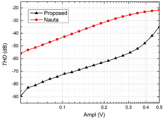
Figure 14.
THD versus input signal amplitude. Input frequency was fixed at 500 Hz.
The spectral content of the output signal is shown in Figure 15, for a particular value of the input amplitude, equal to 400 mV. Due to the symmetry of the circuit, even order harmonics are not present. The ratio of the larger harmonic component (third) with respect to the input tone magnitude is around −47 dB for the proposed solution and −23 dB for the Nauta’s one.
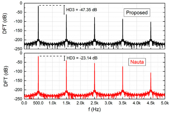
Figure 15.
Output spectra of the S/H shown in Figure 13, employing the proposed amplifier (top) and the Nauta transconductor (bottom), when the input is a 400 mV amplitude, 500 Hz sinusoid.
5. Conclusions
Electrical simulations performed on the designed amplifier confirmed that the proposed CMSL provides correct stabilization of the output CM voltage at both 0.3 V and 0.5 V supply voltages, with less effect on the output differential range than the Nauta transconductor. Despite the larger number of inverters used in the CMSL, the proposed solution requires that only two inverters (Inv5–6) match the output current capability of the inverters in the forward path, while in Nauta’s circuit this requirement applies to all four inverter of the CMSL. This property of the proposed circuit can be used to mitigate the area and power requirements of all the other five inverters forming the CMSL. The simple examples of an SC integrator and an S/H circuit shown in this paper suggested that the proposed amplifier can be successfully used for the implementation of ULV analog discrete-time circuits, with output signal ranges that extends across almost the full rail-to-rail span. The small gain exhibited by the circuit is due to the adoption of minimum-length MOSFETs and could be mitigated by using integrator topologies [5,6] with less sensitivity to the finite amplifier gain.
Author Contributions
Conceptualization, G.M. and L.B.; methodology, A.C. and P.B.; validation, M.C. and L.B.; formal analysis, A.C. and L.B.; investigation, A.C. and G.M.; data curation, M.P.; writing—original draft preparation, G.M., A.C. and L.B.; writing—review and editing, A.C., L.B. and P.B.; supervision, P.B. and M.P. All authors have read and agreed to the published version of the manuscript.
Funding
This research received no external funding.
Conflicts of Interest
The authors declare no conflict of interest.
References
- Amirinasab Nasab, M.; Shamshirband, S.; Chronopoulos, A.T.; Mosavi, A.; Nabipour, N. Energy-Efficient Method for Wireless Sensor Networks Low-Power Radio Operation in Internet of Things. Electronics 2020, 9, 320. [Google Scholar] [CrossRef]
- Hu, H.; Islam, T.; Kostyukova, A.; Ha, S.; Gupta, S. From Battery Enabled to Natural Harvesting: Enzymatic BioFuel Cell Assisted Integrated Analog Front-End in 130nm CMOS for Long-Term Monitoring. IEEE Trans. Circuits Syst. I Regul. Pap. 2019, 66, 534–545. [Google Scholar] [CrossRef]
- Bae, W. CMOS Inverter as Analog Circuit: An Overview. J. Low Power Electron. Appl. 2019, 9, 26. [Google Scholar] [CrossRef]
- Cheng, Q.; Li, W.; Tang, X.; Guo, J. Design and Analysis of Three-Stage Amplifier for Driving pF-to-nF Capacitive Load Based on Local Q-Factor Control and Cascode Miller Compensation Techniques. Electronics 2019, 8, 572. [Google Scholar] [CrossRef]
- Haug, k.; Maloberti, F.; Temes, G.C. Switched-capacitor integrators with low finite-gain sensitivity. Electron. Lett. 1985, 21, 1156–1157. [Google Scholar] [CrossRef]
- Bruschi, P.; Catania, A.; Del Cesta, S.; Piotto, M. A Two-Stage Switched-Capacitor Integrator for High Gain Inverter-Like Architectures. IEEE Trans. Circuits Syst. Ii Express Briefs 2020, 67, 210–214. [Google Scholar] [CrossRef]
- Fazli Yeknami, A. A 300-mV ΔΣ Modulator Using a Gain-Enhanced, Inverter-Based Amplifier for Medical Implant Devices. J. Low Power Electron. Appl. 2016, 6, 4. [Google Scholar] [CrossRef]
- Richelli, A.; Colalongo, L.; Kovacs-Vajna, Z.; Calvetti, G.; Ferrari, D.; Finanzini, M.; Pinetti, S.; Prevosti, E.; Savoldelli, J.; Scarlassara, S. A Survey of Low Voltage and Low Power Amplifier Topologies. J. Low Power Electron. Appl. 2018, 8, 22. [Google Scholar] [CrossRef]
- Nauta, B. A CMOS transconductance-C filter technique for very high frequencies. IEEE J. Solid State Circuits 1992, 27, 142–153. [Google Scholar] [CrossRef]
- Rodovalho, L.H. Push–pull based operational transconductor amplifier topologies for ultra low voltage supplies. Analog Integr. Circuits Signal. Process. 2020. [Google Scholar] [CrossRef]
- Vieru, R.G.; Ghinea, R. Inverter-based ultra low voltage differential amplifiers. In Proceedings of the 34th International Semiconductor Conference (CAS 2011), Sinaia, Romania, 17–19 October 2011. [Google Scholar]
- Chatterjee, S.; Tsividis, Y.; Kinget, P. 0.5-V analog circuit techniques and their application in OTA and filter design. IEEE J. Solid State Circuits 2005, 40, 2373–2387. [Google Scholar] [CrossRef]
- Martin, K.; Sedra, A.S. Strays-insensitive switched-capacitor filters based on bilinear Z-transform. Electron. Lett. 1979, 15, 365–366. [Google Scholar] [CrossRef]
- Dessouky, M.; Kaiser, A. Very Low-Voltage Digital-Audio Δ∑ Modulator with 88-dB Dynamic Range Using Local Switch Bootstrapping. IEEE J. Solid State Circuits 2001, 36, 349–355. [Google Scholar] [CrossRef]
- Benvenuti, L.; Catania, A.; Cicalini, M.; Ria, A.; Piotto, M.; Bruschi, M. A 0.3 V 15 nW 69 dB SNDR Inverter-Based Δ∑ Modulator in 0.18 μm CMOS. In Proceedings of the 15th Conference on Ph.D Research in Microelectronics and Electronics (PRIME), Lausanne, Switzerland, 15–18 July 2019. [Google Scholar]
- Van de Plassche; Rudy, J. CMOS Integrated Analog-to-Digital and Digital-to-Analog Converters, 2nd ed.; Springer US: Boston, MA, USA, 2013. [Google Scholar]
- Centurelli, F.; Monsurrò, P.; Pennisi, S.; Scotti, G.; Trifiletti, A. Design solutions for sample-and-hold circuits in CMOS nanometer technologies. IEEE Trans. Circuits Syst. Ii Express Briefs 2009, 56, 459–463. [Google Scholar] [CrossRef]
© 2020 by the authors. Licensee MDPI, Basel, Switzerland. This article is an open access article distributed under the terms and conditions of the Creative Commons Attribution (CC BY) license (http://creativecommons.org/licenses/by/4.0/).