Article

Demonstration of AlGaN/GaN MISHEMT on Si with Low-Temperature Epitaxy Grown AlN Dielectric Gate

by
Matthew Whiteside
1,*,
Subramaniam Arulkumaran
2,
Yilmaz Dikme
3,
Abhinay Sandupatla
1 and
Geok Ing Ng
1,2,*
1
School of Electrical and Electronic Engineering, Nanyang Technological University, Singapore 639798, Singapore
2
Temasek Laboratories @ NTU, Nanyang Technological University, Singapore 637553, Singapore
3
AIXaTECH GmbH, Thomas-Edison-Str. 5-7, 52499 Baesweiler, Germany
*
Authors to whom correspondence should be addressed.
Electronics 2020, 9(11), 1858; https://doi.org/10.3390/electronics9111858
Submission received: 11 October 2020 / Revised: 28 October 2020 / Accepted: 3 November 2020 / Published: 5 November 2020
(This article belongs to the Special Issue Micro- and Nanotechnology of Wide Bandgap Semiconductors)

Abstract

:
AlGaN/GaN metal-insulator-semiconductor high-electron-mobility transistors (MISHEMT) with a low-temperature epitaxy (LTE)-grown single crystalline AlN gate dielectric were demonstrated for the first time and the post-gate annealing effects at 400 °C were studied. The as-deposited LTE-AlN MISHEMT showed a maximum drain current (IDmax) of 708 mA/mm at a gate bias of 4 V and a maximum extrinsic transconductance (gmmax) of 129 mS/mm. The 400 °C annealed MISHEMT exhibited an increase of 15% in gmmax, an order of magnitude reduction in reverse gate leakage and about a 3% suppression of drain current (ID) collapse. The increase of gmmax by post-gate annealing is consistent with the increase of 2DEG mobility. The suppression of ID collapse and the reduction of gate leakage current is attributed to the reduction of interface state density (5.0 × 1011 cm−2eV−1) between the AlN/GaN interface after post-gate annealing at 400 °C. This study demonstrates that LTE grown AlN is a promising alternate material as gate dielectric for GaN-based MISHEMT application.

1. Introduction

AlGaN/GaN based high-electron-mobility transistors (HEMTs) have demonstrated excellent high-frequency and high-power performance owing to their excellent material properties, such as large breakdown field, wide band gap and high electron mobility [1,2,3,4]. However, two of the major limiting factors that conventional GaN HEMTs with Schottky metal gates suffer from are a high gate leakage current, and current collapse [5]. The high gate-leakage occurs due to the Schottky metal contact, while current collapse is caused by charge trapping at the surface states present on the AlGaN surface. To solve these issues, various materials such as Al2O3 [6,7], HfO2 [8] or ZrO2 [9] have been used as both a passivation layer and gate dielectrics. Among non-oxide insulators, AlN is an attractive high-k dielectric material for III–N metal-insulator-semiconductor high-electron-mobility transistors (MISHEMTs) due to its high breakdown field and high dielectric constant [10,11]. In addition, AlN is of interest due to its high thermal conductivity (200 WK−1m−1), which makes it suitable for use as a passivation layer to suppress the self-heating [12]. AlN has also been reported to help reduce current collapse [13]. There are two main methods used for the deposition of AlN namely metal-organic chemical vapor deposition [14] (MOCVD) and plasma-enhanced atomic layer deposition [15,16] (PEALD). However, the growth temperature of MOCVD (>600 °C) is not desirable for the fabrication of AlGaN/GaN HEMTs. Furthermore, using a lower growth temperature also has the advantage of preventing tensile strain-induced cracking of AlN layer in AlN based MIS-HEMTs [17,18]. PEALD is a different approach to grow AlN films which can form a better interface with GaN at 350 °C but with a low deposition rate [19]. Recently, Dikme et al. [20] realized thick single crystalline AlN layers on Si and sapphire substrates at 200 °C using a novel technique called low-temperature epitaxy (LTE). In this technique, AlN is deposited as a combination of physical vapor deposition (PVD) and chemical vapor deposition (CVD). LTE also allows for thick (~1 µm) crystalline films to be grown at low-temperatures which is compatible with III-V device processing. We have recently reported the properties of interface states for AlGaN/GaN metal-insulator-semiconductor diodes (MIS-diodes) using the LTE grown AlN [21,22] So far, no reports have discussed the AlGaN/GaN MISHEMTs with LTE-AlN and its post-gate annealing effects. In this paper, we report AlGaN/GaN MISHEMTs on Si substrate with LTE grown AlN through DC, pulsed I-V and interface trap characterization and analysis.

2. Materials and Methods

The AlGaN/GaN HEMT structure on Si (111) substrate was grown by MOCVD. It consists of i-GaN (2 nm) cap layer, i-Al0.27Ga0.73N (18 nm) barrier layer, i-GaN (800 nm) buffer layer and transition layer (1400 nm). The resistivity of the Si substrate is >10,000 Ω.cm. Hall samples of (i) as-grown HEMT without LTE-AlN, (ii) HEMT with as-deposited ~8 nm LTE-AlN, (iii) HEMT with LTE-AlN annealed at 400 °C and (iv) HEMT with LTE-AlN annealed at 450 °C were prepared and their results at room temperature are summarized in Table 1. The MISHEMT fabrication process started with mesa isolation by reactive ion etching (RIE) using a Cl2/BCl3 mixture. The ohmic contacts consisting of Ti/Al/Ni/Au (20/120/40/50 nm) was deposited followed by rapid thermal annealing at 825 °C for 30 s in an N2 atmosphere. Transmission line measurements showed a contact resistance of 0.4 Ω mm. Next, the gate dielectric layer using single crystalline AlN with a thickness of ~8 nm was deposited at 200 °C by LTE. The thickness of the deposited LTE-AlN has previously been confirmed by TEM and is reported elsewhere [22]. The novel growth method combines physical vapor deposition (PVD) and chemical vapor deposition (CVD). The Al source is solid Al with a purity of 5N, while the N source is N2 gas with purity of 5N8. The N was activated by a linear ion gun close to the sample surface and the Al was sputtered in a way that its beam overlaps with the ion gun beam. The substrate temperature was in the range of 200–225 °C and the deposition pressure was in the upper 10−3 mbar range with a total power density of around 5–7 W/cm2. Before the deposition, the sample was cleaned with a weak Ar/H2 plasma to remove the native oxide. More details of the growth conditions can be found in the paper by Dikme et al. [20,21].
The gate metal stack Ni/Au (50/200 nm) was subsequently formed on the LTE grown AlN by electron beam evaporation. Finally, metal thickening (Ti/Au 10/400 nm) was also performed after AlN etching by Cl2/BCl3/Ar (40/20/10 sccm) plasma. The inset of Figure 1a shows the cross-sectional schematic diagram of the fabricated MISHEMTs with LTE-grown AlN. For this study, we have used device dimensions of Lg/Lsg/Lgd/Wg = 2/2/2/(2 × 100) µm. To study the post-gate annealing effects a MISHEMT sample with ~8 nm of LTE-AlN were annealed at 400 °C in a N2 atmosphere using rapid thermal annealing process. A post-gate annealing temperature of 400 °C was chosen as there was minimal changes to the Hall parameters after post deposition annealing at 450 °C (see Table 1). A lower temperature is also beneficial, as higher temperatures have previously been shown to cause degradation of Ni/Au gates [23,24].

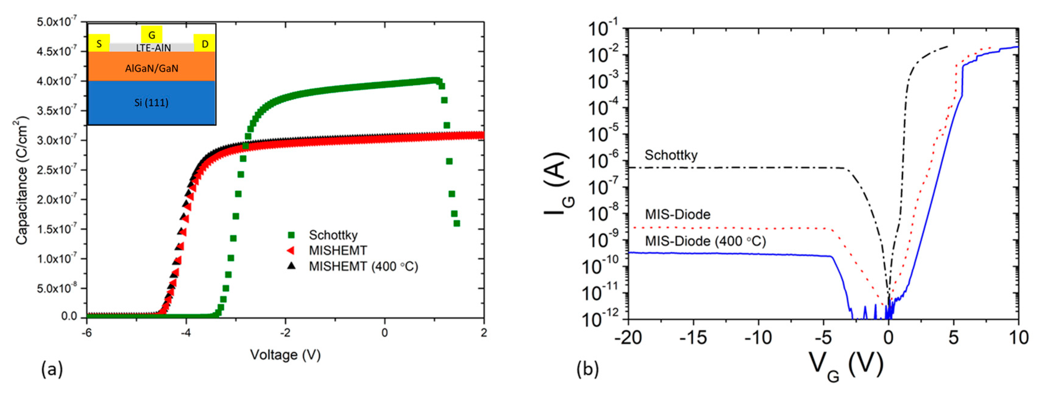
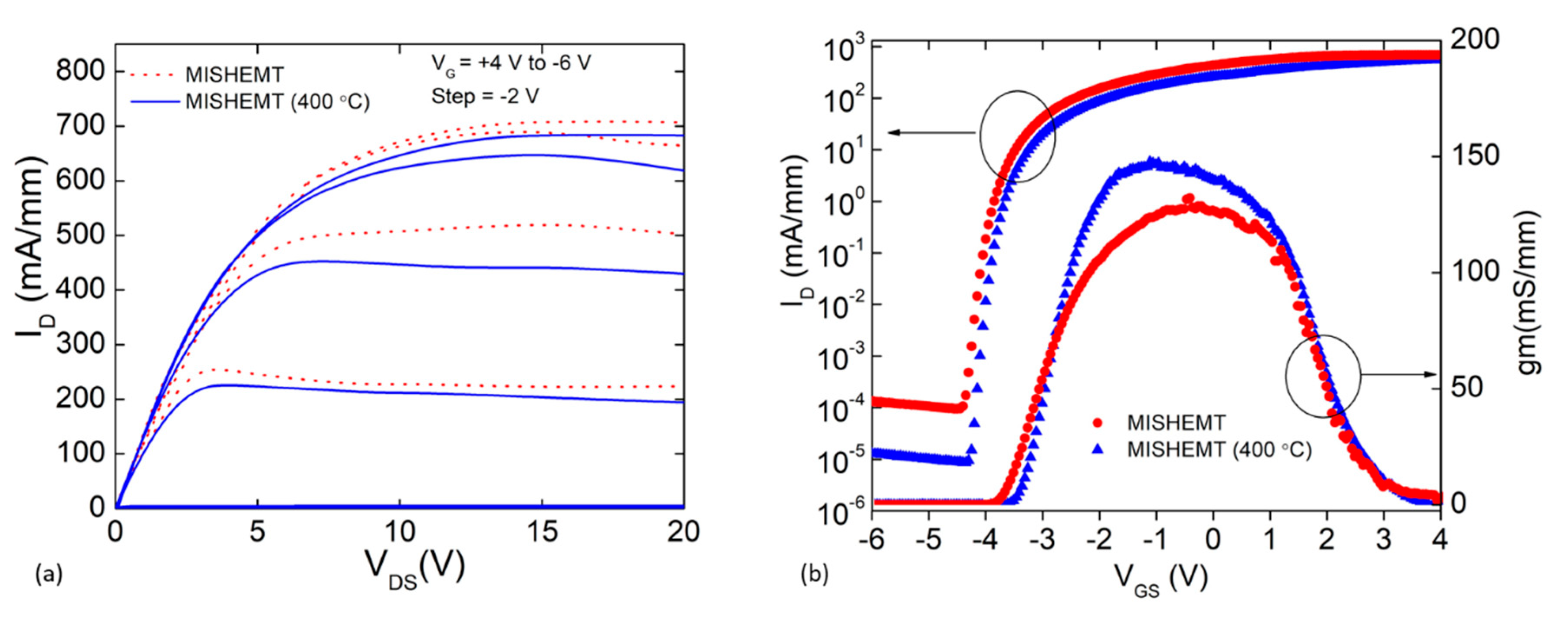
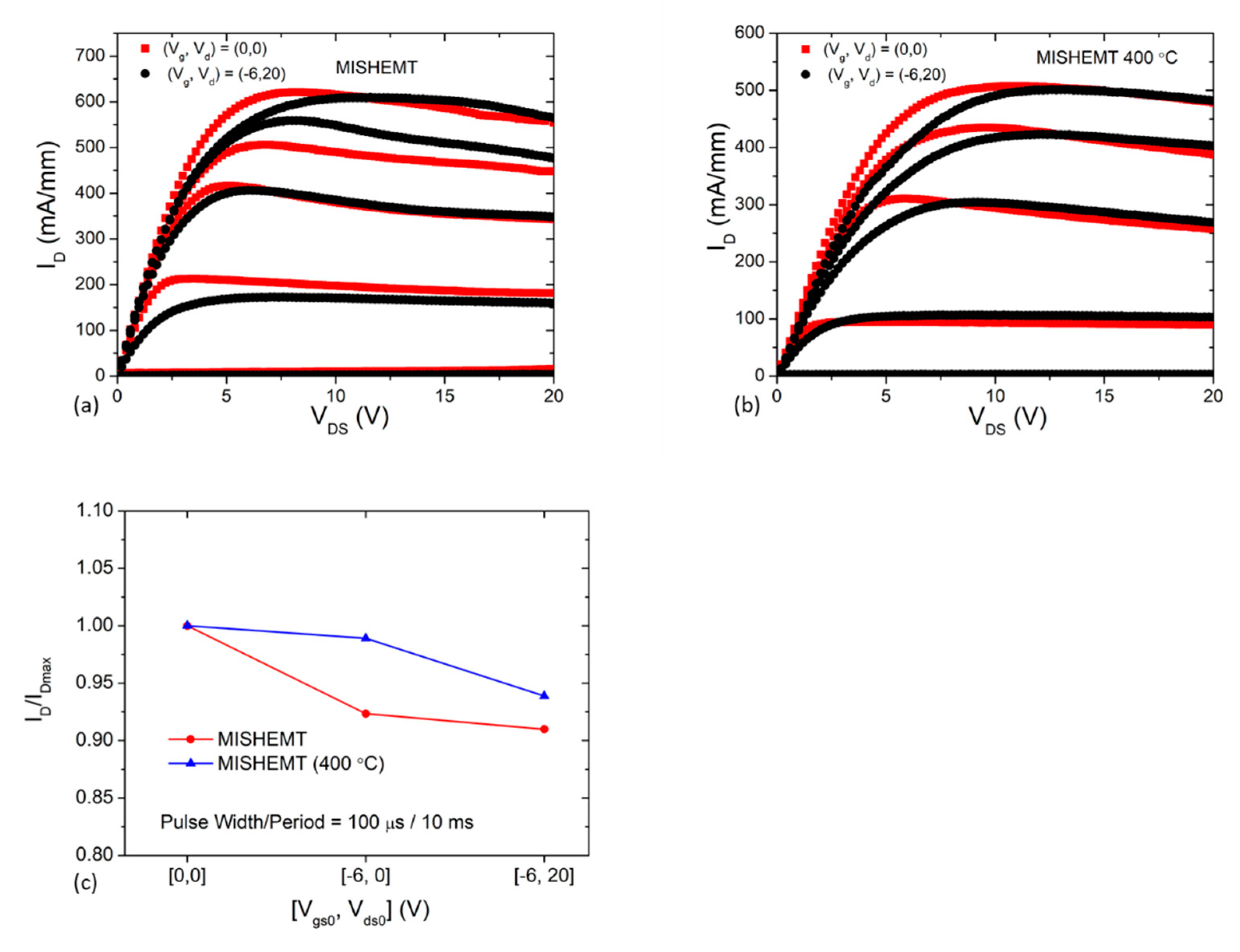
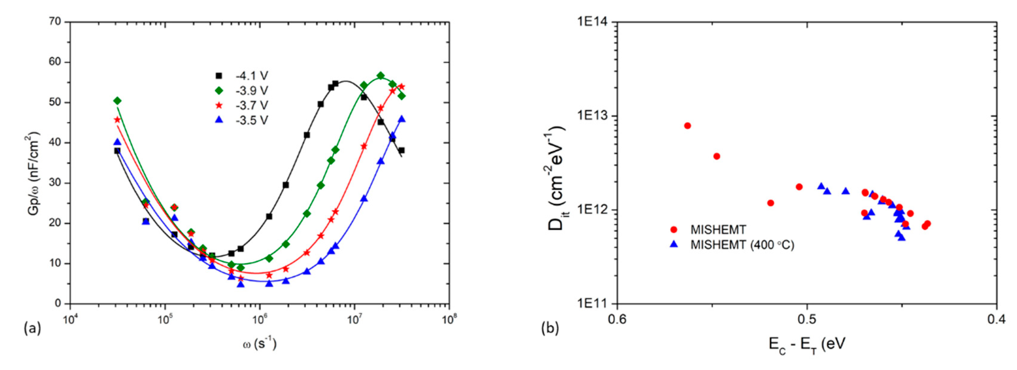
3. Results and Discussion

Figure 1 shows (a) the capacitance-voltage (C-V) and (b) gate leakage current (Igleak) characteristics of Schottky diode (MS-diode), LTE-AlN MIS-diode with and without post-gate annealing. At zero-bias, the capacitance density of 373 nF/cm2 and 302 nF/cm2 for 200 µm diameter conventional Schottky diode and MIS-diode were obtained, respectively. After annealing, there is no significant change in capacitance density at 0 V. With reference to Schottky diode, the LTE-AlN MIS-diode exhibited 2 orders of magnitude lower Igleak at −20 V (Figure 1b). After post-gate annealing at 400 °C, MIS-diodes exhibited about an order of magnitude further reduction in Igleak. The improvement in Igleak is attributed to the improvement of interface properties of LTE-AlN on GaN/AlGaN after the 400 °C annealing.
Figure 2 shows (a) current–voltage (Ids-Vds) and (b) transfer characteristics of LTE-AlN/AlGaN/GaN MISHEMTs without and with post-gate annealing at 400 °C. The as-deposited AlN MISHEMT showed a maximum drain current (IDmax) of 708 mA/mm at a gate bias of 4 V and a maximum extrinsic transconductance (gmmax) of 129 mS/mm. After annealing, MISHEMT exhibited IDmax of 684 mA/mm at a gate bias of 4 V and gmmax of 148 mS/mm. The decrease in IDmax after annealing originates from a change in two-dimensional electron gas (2DEG) carrier concentration (ns), as ID ∝ ns. As shown in Table 1, after annealing at 400 °C, ns was found to decrease by 9% (from 9.89 × 1012 cm−2 to 9.02 × 1012 cm−2) which results in the 9% reduction in IDmax. Similarly, the 15% improvement of gmmax after post-gate annealing is attributed to an increase in electron mobility as well as a reduction of interface states [25]. This is attributed to a reduction in Coulomb scattering from the dielectric layer near the AlGaN/GaN interface [26]. The enhanced mobility was confirmed by Hall measurements, which shows an ~10% improvement (from 1210 cm2V−1s−1 to 1330 cm2V−1s−1) in 2DEG Hall mobility (µn), as seen in Table 1. From the Figure 2b, it is clear that AlN MISHEMT exhibited an order of magnitude improvement in the device ION/IOFF ratio after the post-gate annealing at 400 °C, which is due to the reduction of drain current at OFF-state. This is possibly caused by a reduction on traps at the AlN/GaN interface reducing the available leakage current conduction paths. The threshold voltages (Vth) of the devices were measured at −3.95 V and −3.8 V for as-deposited MISHET and post-gate annealed MISHEMT at 400 °C, respectively. Vth can be expressed as
V th = V th 0 Q it C AlN
where Vth0 is the threshold voltages without any interface states, Qit is the interface-trapped charge density and CAlN is the capacitance of the AlN layer. After annealing at 400 °C there is a minimal positive shift in threshold voltage which could be caused by a slight reduction of interface traps at LTE-AlN/GaN interface. This is verified by the frequency-dependent conductance measurements discussed in the later section. A similar occurrence was also reported after post-gate annealing by Zhou et al. for Al2O3 and Shih et al. for HfO2 [8,25]. In these cases, it was postulated that the positive Vth shift was caused by a reduction in positively charged traps and interface traps or positive fixed/mobile charges, and was confirmed by a reduction in calculated interface states after annealing. A benchmarking table between these devices and those published elsewhere can be seen in Table 2 [15,27,28,29].
Figure 3 shows pulsed ID-VD characteristics of (a) as-deposited MISHEMTs with LTE-AlN and (b) MISHEMTs with post-gate annealing at 400 °C. The devices were subjected to the pulse width/period of 100 µs/10ms and quiescent biases of (Vgs0, Vds0) = (0, 0) and (−6, 20) V was used for the pulsed I-V measurements. The as-deposited LTE-AlN MISHEMT exhibited a ID/IDmax ratio of 0.91 for both quiescent biases (Vgs0, Vds0) = (0, 0) and (−6, 20). This indicates that the devices exhibited around 9% drain current (ID) collapse. After annealing at 400 °C, the ID/IDmax ratio of MISHEMT increases to 0.94. Therefore, about 3% ID collapse was suppressed after post-gate annealing at 400 °C. The improvement in current collapse in 400 °C annealed MISHEMT is attributed to the reduction of interface states at the AlN/GaN interface.
In order to quantify the amount of interface states at the LTE-AlN/GaN interfaces, frequency-dependent conductance measurements were performed at selected biases to estimate the density of interface states (Dit) and trap time constant (τit). The frequency was varied from 1 kHz to 5 MHz over a wide range of gate voltages (Vg). Figure 4a shows the typical Gp/ω versus ω graph of LTE-AlN MISHEMT with post-gate annealed at 400 °C measured at different Vg values between −4.1 V to −3.5 V. The Dit calculations were performed using the conductance-frequency method, which is widely used for interface calculations [21,30,31]. The two peak regions in the Gp/ω plots correspondingly indicate the presence of both low frequency (slow traps) and high frequency (fast traps). The exhibited fast traps are associated interface traps of the AlGaN/GaN hetero-interface [15,32], while the observed slow traps are associated with the AlN/GaN interface. The estimated Dit is shown in Figure 4b for the as-deposited LTE-AlN MIS-diode, as well as the MIS-diodes with post-gate annealing at 400 °C. The minimum Dit were estimated as 7.6 × 1011 cm−2eV−1 and 5.0 × 1011 cm−2eV−1 for the as-deposited MIS-diode and MIS-diode with post-gate annealing at 400 °C, respectively. With reference to as-deposited MIS-diode, a reduction of Dit (24%) has been observed in the MIS-diode after post-gate annealing at 400 °C. This reduction of interface traps can be associated with the suppression of ID collapse. Annealing at 400 °C helps to reduce the slow deep level traps thus reducing the remote Coulomb scattering from the AlN layer and improving the mobility.

4. Conclusions

In summary, AlGaN/GaN MISHEMTs on Si has been demonstrated for the first time with LTE grown AlN as a dielectric layer. The influence of post-gate annealing at 400 °C was also studied using DC, pulsed I-V and interface state characteristics. After the LTE-AlN deposition the LTE-AlN MISHEMT showed a maximum drain current (IDmax) of 708 mA/mm at a gate bias of 4 V and a maximum extrinsic transconductance (gmmax) of 129 mS/mm. By employing a post-gate annealing scheme at 400 °C in an N2 atmosphere there was about a 15% of increase in gmmax and an order of magnitude reduction of gate leakage. About a 3% improvement of ID collapse suppression was also observed after post-gate annealing at 400 °C. The reduction of Igleak and ID collapse could be due to the reduction of interface state density of about 25%. This study indicates that the optimized post-gate annealing, which in our case is at 400 °C, is a viable way to have improved device characteristics in AlGaN/GaN MISHEMTs with LTE grown AlN.

Author Contributions

Conceptualization, M.W., S.A. and G.I.N.; methodology, M.W. and Y.D.; formal analysis, M.W. and A.S.; investigation, M.W.; resources, Y.D., S.A. and G.I.N.; data curation, M.W. and A.S.; writing—original draft preparation, M.W.; writing—review and editing, S.A., and G.I.N.; visualization, M.W.; supervision, G.I.N.; project administration, G.I.N. All authors have read and agreed to the published version of the manuscript.

Funding

This research received no external funding.

Conflicts of Interest

The authors declare no conflict of interest.

References

  1. Kumar, V.; Lu, W.; Schwindt, R.; Kuliev, A.; Simin, G.; Yang, J.; Khan, M.A.; Adesida, I. AlGaN/GaN HEMTs on SiC with fT of over 120 GHz. IEEE Electron Device Lett. 2002, 23, 455–457. [Google Scholar] [CrossRef]
  2. Simin, G.; Hu, X.; Ilinskaya, N.; Kumar, A.; Koudymov, A.; Zhang, J.; Asif Khan, M.; Gaska, R.; Shur, M.S. 7.5kW/mm2 current switch using AlGaN/GaN metal-oxide-semiconductor heterostructure field effect transistors on SiC substrates. Electron. Lett. 2000, 36, 2043–2044. [Google Scholar] [CrossRef] [Green Version]
  3. Adivarahan, V.; Gaevski, M.; Sun, W.H.; Fatima, H.; Koudymov, A.; Saygi, S.; Simin, G.; Yang, J.; Khan, M.A.; Tarakji, A.; et al. Submicron Gate. IEEE Electron Device Lett. 2003, 24, 541–543. [Google Scholar] [CrossRef]
  4. Kordoš, P.; Heidelberger, G.; Bernát, J.; Fox, A.; Marso, M.; Lüth, H. High-power SiO2/AlGaN/GaN metal-oxide-semiconductor heterostructure field-effect transistors. Appl. Phys. Lett. 2005, 87, 143501. [Google Scholar] [CrossRef] [Green Version]
  5. Mizuno, S.; Ohno, Y.; Kishimoto, S.; Maezawa, K.; Mizutani, T. Large gate leakage current in AlGaN/GaN high electron mobility transistors. Jpn. J. Appl. Phys. Part 1 Regul. Pap. Short Notes Rev. Pap. 2002, 41, 5125–5126. [Google Scholar] [CrossRef]
  6. Kim, K.W.; Jung, S.D.; Kim, D.S.; Im, K.S.; Kang, H.S.; Lee, J.H.; Bae, Y.; Kwon, D.H.; Cristoloveanu, S. Charge trapping and interface characteristics in normally-off Al2O3/GaN-MOSFETs. Microelectron. Eng. 2011, 88, 1225–1227. [Google Scholar] [CrossRef]
  7. Liu, Z.H.; Ng, G.I.; Arulkumaran, S.; Maung, Y.K.T.; Teo, K.L.; Foo, S.C.; Sahmuganathan, V.; Xu, T.; Lee, C.H. High microwave-noise performance of AlGaN/GaN MISHEMTs on silicon with Al2O3 Gate Insulator Grown by ALD. IEEE Electron Device Lett. 2010, 31, 96–98. [Google Scholar] [CrossRef]
  8. Shih, C.F.; Hung, K.T.; Hsiao, C.Y.; Shu, S.C.; Li, W.M. Investigations of GaN metal-oxide-semiconductor capacitors with sputtered HfO2 gate dielectrics. J. Alloys Compd. 2009, 480, 541–546. [Google Scholar] [CrossRef]
  9. Ye, G.; Wang, H.; Arulkumaran, S.; Ng, G.I.; Hofstetter, R.; Li, Y.; Anand, M.J.; Ang, K.S.; Maung, Y.K.T.; Foo, S.C. Atomic layer deposition of ZrO2 as gate dielectrics for AlGaN/GaN metal-insulator-semiconductor high electron mobility transistors on silicon. Appl. Phys. Lett. 2013, 103, 142109. [Google Scholar] [CrossRef]
  10. Shih, H.A.; Kudo, M.; Suzuki, T.K. Analysis of AlN/AlGaN/GaN metal-insulator-semiconductor structure by using capacitance-frequency-temperature mapping. Appl. Phys. Lett. 2012, 101, 043501. [Google Scholar] [CrossRef]
  11. Kudo, M.; Shih, H.-A.; Akabori, M.; Suzuki, T. Fabrication and analysis of AlN/GaAs(001) and AlN/Ge/GaAs(001) metal–insulator–semiconductor structures. Jpn. J. Appl. Phys. 2012, 51, 02BF07. [Google Scholar] [CrossRef]
  12. Tsurumi, N.; Ueno, H.; Murata, T.; Ishida, H.; Uemoto, Y.; Ueda, T.; Inoue, K.; Tanaka, T. AlN passivation over AlGaN/GaN HFETs for surface heat spreading. IEEE Trans. Electron Devices 2010, 57, 980–985. [Google Scholar] [CrossRef]
  13. Huang, S.; Jiang, Q.; Yang, S.; Zhou, C.; Chen, K.J. Effective passivation of AlGaN/GaN HEMTs by ALD-grown AlN thin film. IEEE Electron Device Lett. 2012, 33, 516–518. [Google Scholar] [CrossRef]
  14. Freedsman, J.J.; Kubo, T.; Egawa, T. Effect of AlN growth temperature on trap densities of in-situ metal-organic chemical vapor deposition grown AlN/AlGaN/GaN metal-insulator-semiconductor heterostructure field-effect transistors. AIP Adv. 2012, 2, 022134. [Google Scholar] [CrossRef]
  15. Zhu, J.J.; Ma, X.H.; Xie, Y.; Hou, B.; Chen, W.W.; Zhang, J.C.; Hao, Y. Improved interface and transport properties of AlGaN/GaN MIS-HEMTs with peald-grown AlN gate dielectric. IEEE Trans. Electron Devices 2015, 62, 512–518. [Google Scholar] [CrossRef]
  16. Huang, S.; Jiang, Q.; Yang, S.; Tang, Z.; Chen, K.J. Mechanism of PEALD-Grown AlN passivation for AlGaN/GaN HEMTs: Compensation of interface traps by polarization charges. IEEE Electron Device Lett. 2013, 34, 193–195. [Google Scholar] [CrossRef]
  17. Hashizume, T.; Alekseev, E.; Pavlidis, D.; Boutros, K.S.; Redwing, J. Capacitance–voltage characterization of AlN/GaN metal–insulator–semiconductor structures grown on sapphire substrate by metalorganic chemical vapor deposition. J. Appl. Phys. 2000, 88, 1983–1986. [Google Scholar] [CrossRef] [Green Version]
  18. Imanaga, S.; Nakamura, F.; Kawai, H. Current–voltage characteristics of AlN/GaN heterostructure metal insulator semiconductor diode. Jpn. J. Appl. Phys. 2001, 40, 1194–1198. [Google Scholar] [CrossRef]
  19. Cao, D.; Cheng, X.; Xie, Y.H.; Zheng, L.; Wang, Z.; Yu, X.; Wang, J.; Shen, D.; Yu, Y. Effects of rapid thermal annealing on the properties of AlN films deposited by PEALD on AlGaN/GaN heterostructures. RSC Adv. 2015, 5, 37881–37886. [Google Scholar] [CrossRef] [Green Version]
  20. Sinhoff, V.; Diikme, Y. Low Temperature Epitaxy (LTE)—A novel approach for the volume production of GaN based devices. In Proceedings of the International Conference and Exhibition of the APE Automotive Power Electronics, Paris, France, 26–27 April 2017; Volume 1. [Google Scholar]
  21. Whiteside, M.; Ng, G.I.; Arulkumaran, S.; Ranjan, K.; Dikme, Y. Low temperature epitaxy grown AlN metal-insulator-semiconductor diodes on AlGaN/GaN HEMT structure. In Proceedings of the 2019 Electron Devices Technology and Manufacturing Conference (EDTM), Singapore, 12–15 March 2019; IEEE: New York, NY, USA, 2019; pp. 103–105. [Google Scholar]
  22. Whiteside, M.; Arulkumaran, S.; Dikme, Y.; Sandupatla, A.; Ng, G.I. Improved interface state density by low temperature epitaxy grown AlN for AlGaN/GaN metal-insulator-semiconductor diodes. Mater. Sci. Eng. B Solid-State Mater. Adv. Technol. 2020, 262, 114707. [Google Scholar] [CrossRef]
  23. Arulkumaran, S.; Egawa, T.; Ishikawa, H.; Umeno, M.; Jimbo, T. Effects of annealing on Ti, Pd, and Ni/n-Al0.11Ga0.89N Schottky diodes. IEEE Trans. Electron Devices 2001, 48, 573–580. [Google Scholar] [CrossRef]
  24. Fang, L.; Tao, W.; Bo, S.; Sen, H.; Fang, L.; Nan, M.; Fu-Jun, X.; Peng, W.; Jian-Quan, Y. Thermal annealing behaviour of Al/Ni/Au multilayer on n-GaN schottky contacts. Chin. Phys. B 2009, 18, 1618–1621. [Google Scholar] [CrossRef]
  25. Zhou, H.; Ng, G.I.; Liu, Z.H.; Arulkumaran, S. Improved device performance by post-oxide annealing in atomic-layer-deposited Al2O3/AlGaN/GaN metal–insulator–semiconductor high electron mobility transistor on Si. Appl. Phys. Express 2011, 4, 104102. [Google Scholar] [CrossRef]
  26. Liu, Z.H.; Ng, G.I.; Arulkumaran, S.; Maung, Y.K.T.; Teo, K.L.; Foo, S.C.; Sahmuganathan, V. Improved two-dimensional electron gas transport characteristics in AlGaN/GaN metal-insulator-semiconductor high electron mobility transistor with atomic layer-deposited Al2O3 as gate insulator. Appl. Phys. Lett. 2009, 95, 223501. [Google Scholar] [CrossRef]
  27. Liu, X.-Y.; Zhao, S.-X.; Zhang, L.-Q.; Huang, H.-F.; Shi, J.-S.; Zhang, C.-M.; Lu, H.-L.; Wang, P.-F.; Zhang, D.W. AlGaN/GaN MISHEMTs with AlN gate dielectric grown by thermal ALD technique. Nanoscale Res. Lett. 2015, 10, 109. [Google Scholar] [CrossRef] [Green Version]
  28. Hwang, Y.-H.; Liu, L.; Velez, C.; Ren, F.; Gila, B.P.; Hays, D.; Pearton, S.J.; Lambers, E.; Kravchenko, I.I.; Lo, C.-F.; et al. GaN metal–insulator–semiconductor high-electron-mobility transistor with plasma enhanced atomic layer deposited AlN as gate dielectric and passivation. J. Vac. Sci. Technol. B Nanotechnol. Microelectron. Mater. Process. Meas. Phenom. 2013, 31, 052201. [Google Scholar] [CrossRef]
  29. Chen, T.; Jiao, G.; Li, Z.; Li, F.; Shao, K.; Yang, N. AlGaN/GaN MIS HEMT with AlN dielectric. In Proceedings of the 2006 International Conference on Compound Semiconductor Manufacturing Technology CS MANTECH Conference, Vancouver, BC, Canada, 24–27 April 2006; pp. 227–230. [Google Scholar]
  30. Kordoš, P.; Stoklas, R.; Gregušová, D.; Gaži, Š.; Novák, J. Trapping effects in Al2O3/AlGaN/GaN metal-oxide-semiconductor heterostructure field-effect transistor investigated by temperature dependent conductance measurements. Appl. Phys. Lett. 2010, 96, 013505. [Google Scholar] [CrossRef]
  31. Quan, S.; Hao, Y.; Ma, X.-H.; Yu, H.-Y. Investigation of AlGaN/GaN fluorine plasma treatment enhancement-mode high electronic mobility transistors by frequency-dependent capacitance and conductance analysis. Chin. Phys. B 2011, 20, 018101. [Google Scholar] [CrossRef]
  32. Ranjan, K.; Arulkumaran, S.; Ng, G.I. Investigations of temperature-dependent interface traps in AlGaN/GaN HEMT on CVD-diamond. Appl. Phys. Express 2019, 12, 106506. [Google Scholar] [CrossRef]
Figure 1. (a) C-V characteristics and (b) two terminal Igleak-Vg (200 um diameter diodes) characteristics of Ni/AlGaN/GaN Schottky diode, as-deposited LTE-AlN/AlGaN/GaN metal-insulator-semiconductor diode [22] and post-gate annealed MIS-diode at 400 °C. Inset: Schematic cross-sectional diagram of fabricated AlGaN/GaN MISHEMTs with LTE grown AlN on Si substrate.
Electronics 09 01858 g001
Figure 2. (a) DC IDS-VDS and (b) transfer characteristics of as-deposited LTE-AlN/AlGaN/GaN MISHEMT and post-gate annealed MISHEMT at 400 °C.
Electronics 09 01858 g002
Figure 3. Pulsed IDS-VDS characteristics at quiescent bias points of (Vgs0, Vds0) = (0, 0), (−6, 20) for (a) LTE-AlN MISHEMTs, (b) 400 °C annealed MISHEMTs and (c) normalized ID with IDmax for as-deposited LTE-AlN/AlGaN/GaN MISEMT and annealed MISHEMT at 400 °C vs. the quiescent bias points (Vgs0, Vds0) = (0, 0), (−6, 0), (−6, 20) V.
Electronics 09 01858 g003
Figure 4. (a) Gp/ω versus radial frequency plot for different gate voltages of post-gate annealed LTE-AlN MIS-diode at 400 °C (solid lines are fitting curves). (b) Distribution of interface state density as a function of the gate voltage of as-deposited LTE-AlN MIS-diodes [22] and post-gate annealed MIS-diodes at 400 °C.
Electronics 09 01858 g004
Table 1. 2DEGproperties of AlGaN/GaN with and without AlN and its post deposition annealing at 400 °C and 450 °C for 300 s in N2.
2DEG ParametersAlGaN/GaN HEMT Structure
Without
LTE-AlN [22]
With LTE-AlN
As-dep. [22]Annealing Temperature °C
400450
Sheet Resistance (Ω/□)591523520512
Hall Mobility (cm2V−1s−1)1440121013301360
Sheet Carrier Concentration (×1012 cm−2)7.359.899.028.76
Table 2. A benchmarking table for MISHEMT on AlGaN/GaN using AlN as a gate dielectric layer.
ReferenceThickness (nm)SubstrateDeposition MethodDevice Dimensions Lg/Wg (µm)Idmax (mA/mm)gmmax (mS/mm)On/Off Ratio (Orders of Magnitude)
[15]10.6Si ALD2.5/60563 @ 5V87~5
[27]10SapphireALD1/200600 @ 4V127~9
[28]20SapphirePEALD0.5/50~1050 @ 2 V289~3
[29]8SiCReactive Sputtering0.4/200~1250 @ 2 V260~3
This work8SiLTE2/(2 × 100)684 @ 4V148 ~8
Publisher’s Note: MDPI stays neutral with regard to jurisdictional claims in published maps and institutional affiliations.

