1. Introduction
The Internet of Things (IoT) requires standardized protocols to integrate heterogeneous devices so that the data transmitted from one end to the other can be interpreted and disseminated, allowing the interconnection of smart devices. It was estimated that in 2010 the number of devices connected to the Internet exceeded the number of people connected by more than six times. Since then, the number of mobile and IoT devices continues to grow at a rapid rate [
1]. Taking advantage of the IoT paradigm and the connectivity it enables, new applications are continually appearing for public service, industry, finance, and the end user. The exchange of information between IoT devices is carried out in local networks formed by sensors and actuators. These networks are managed as Wireless Sensor Networks (WSNs). In IoT networks, there are millions of interconnected local WSNs, and within each WSN there are different types of smart devices or wireless sensor nodes, which exchange information using different protocols. Therefore, a wireless sensor node must be capable of processing, in addition to transmitting and receiving information from different wireless sensor nodes or from the Internet.
An application of great interest in the IoT domain is smart street lighting systems, which are defined as a networked street lighting system, equipped with sensors and actuators, that integrates a wide set of nodes and connectivity interfaces, and that, in particular, use advanced and multipurpose communication infrastructures to illuminate public spaces and roads. In addition, they allow one to control and monitor modern and heterogeneous lighting devices. Therefore, WSNs provide a shared medium for sensors and actuators to transfer data in smart street lighting systems [
2].
In the context of IoT and smart street lighting, nodes must support numerous sensor connections with different interfaces. In addition, the processing capacity that is required to handle the data acquired by the sensors is increasingly high, so even in some cases it is necessary to apply Artificial Intelligence and Machine Learning techniques. On the other hand, the street lighting system data network is increasingly used as a backbone network to offer other services and functions, such as predictive maintenance, people flow control, environmental control, parking space search, etc. [
3,
4,
5]. Networked streetlights should provide a basis for smart city applications such as urban planning, traffic management, identification of mobility patterns, surveillance, security and emergency assistance, etc. [
4,
6,
7,
8,
9,
10]. In addition, to improve the visibility and the controllability of the system, the nodes perform tasks typical for the network of which they are part, such as packet routing and flow control [
2,
5,
11].
In order to cover the aforementioned applications, the nodes must continually increase their performance and their number of connections to sensors, in addition to maintaining a low power consumption, cost and ease of replacement and maintenance, all without forgetting the robust and reliable control that they must carry out on the lamps. One of the main interfaces created for lighting systems is the DALI, specially developed to digitally control luminaires, electronic ballasts, and dimmable fluorescent lights. In Europe, it is used to solve energy problems, mainly for commercial and industrial purposes. It is part of the IEC 60929 [
12] specification and were modified by IEC 62386 standard [
13] of electronic ballast. DALI-type ballasts can operate at lower power levels than standard magnetic ballasts [
14] and DALI supports the replacement of adjustable ballasts and luminaires from different manufacturers [
15]. The DALI protocol offers bidirectional communication, thus ensuring a more reliable and secure transmission of data, compared to other lighting control protocols [
16]. Some of the main advantages of using the DALI protocol are:
Detection of electrical faults or lamp failures.
Lamp status notification.
Lamp power level regulation.
Maximum or default values for lamp operating tolerances.
Power consumption optimization.
Capability of sending information about the electrical characteristics of the lamp (voltage, current and power).
Individual or group control, by addressing with Identifiers (ID).
Lower system cost and more functions compared to 1–10 V systems.
Lighting systems based on the DALI protocol are the most suitable for street lighting systems due to the indicated advantages, allowing digital lighting control operations and other management tasks (for example, energy monitoring) to be carried out, in addition to achieving energy savings and adapting to the lighting conditions and the needs of each moment [
17,
18,
19,
20]. However, the Microcontrollers (MCUs) used in the nodes that are part of the lighting control networks do not have this integrated interface, so in most cases, the DALI protocol has been implemented by Software (SW) and used in different lighting prototypes [
21,
22]. The implementation of DALI by SW as a virtual peripheral has limitations, such as the consumption of resources (usually timers) of the MCU and the large processing time that leads to an “inappropriate synchronization” to transmit control data to the network and communicate with other devices.
The implementation of “virtual peripherals” through SW has strict time requirements, which implies reserving a certain processing time in addition to consuming Hardware Resources (HW) of the MCU. The integration of virtual peripherals as part of an application makes excessive use of interrupt services routines and requires careful SW development. Any new service that is implemented on the node should consider the impact on virtual interfaces and peripherals made by the SW. Therefore, a need arises to free the MCU from the DALI implementation as a virtual peripheral. One of the simplest and most efficient ways to achieve this is to create a bridge between the MCU and the DALI bus. This bridge should communicate with the MCU through a single link such as the Universal Asynchronous Receiver–Transmitter (UART) or Serial Peripheral Interface (SPI), which are implemented in almost all commercial MCUs.
One of the options to implement a DALI Bridge is the HW implementation. It has many advantages over the SW implementation. All real time problems that may appear in the bridge design by SW will disappear, if implemented by HW. In addition, the implementation by HW provides other advantages to implement the lower layers of communications that will be detailed in this paper. The construction of tasks by HW is not new and is the basis of the HW/SW codesign [
23]. It is one of the best options when these tasks have strict real-time requirements, are parallel in nature, or must have high performance and limited power consumption.
One alternative for the development of an ad-hoc peripheral by HW is a FPGA. This device allows HW reconfiguration, even dynamically, so it is commonly used to perform overly complex processing tasks, which must have an adequate real-time response. An FPGA enables the implementation by HW of any peripheral or specific application circuit and up to one or more Central Processing Unit (CPU), all working in parallel. Hence, it is a very versatile device, which allows one to implement highly efficient and customized digital electronic systems, compared to a classic CPU. The advantages of FPGAs in terms of cost, size and power consumption facilitate their use in platforms for wireless communications [
24,
25]. Their evolution has led them to be employed to reduce time and cost in the development of complex communication systems for satellites and spacecrafts that use high-speed protocols [
26].
The objective of this work is the HW implementation of the DALI protocol (DALI Bridge) through a low-cost FPGA in a Wireless Sensor Node for Street Lighting applications in IoT, that allows for the execution of the DALI protocol in real time and that is suitable for the needs of the application in terms of the integration of devices and sensors.
This paper is structured as follows:
Section 2 emphasizes previous related work;
Section 3 describes the materials and methodology of the proposed design;
Section 4 presents the experimental results of the DALI Bridge FPGA-based implementation and provides both a brief discussion of the experimentation performed and the overall performance of the implementation; in
Section 5, the conclusions are established.
2. Related Work
The innovation and evolution of smart street lighting systems have historically been supported in the WSNs, for example, in [
27] a wireless street lighting system was proposed to verify and guarantee the optimal parameters of the system and the state of the street lamps; and also to optimize control, as in [
28], where an autonomous street lighting system is proposed to collect information for management and maintenance.
Regarding street lighting systems, works are identified based on the use of MCUs and the help of various components to control streetlights. For example, in [
29], attenuation profiles of on/off sequences are configured, having the disadvantage of a slow execution of the program that prevents adequate communication in the streetlight.
Desktop computers have been used to control lighting, as in [
30], where they control street lighting and transmit information remotely. They have also been used to propose prototypes, as in [
31], where they run a perceptual light automation algorithm. A similar case is the wireless system for the control of street light presented in [
32], where an 8-bit AVR MCU is programmed to control all the necessary interfaces. Another street lighting system reported in [
33] tries to support IoT applications for intelligent transport, where a communication manager is performed by SW to receive frames and process the information. From the analysis of the mechanisms used for the communication interfaces in the aforementioned lighting systems, we can observe that these interfaces are dependent on a collection of libraries, source code, different tools and applications determined by the device where the program is executed, which limits its operation.
Programming the DALI protocol as a bridge in devices such as Programmable Logic Controllers (PLCs) or commercial development boards reduces its computing capacity due to the need to execute different mandatory processes related to the DALI protocol. Furthermore, the high-power consumption and cost of the devices make them impractical for the portability and flexibility requirements of a wireless sensor node for IoT applications. In [
34], after analyzing various lighting control methods, it was determined that the DALI protocol is the most convenient to use. As an analysis case, they control the lighting with a PLC using a DALI soft-gateway to convert from the Modbus protocol of the PLC to the DALI protocol. Another case is presented in [
35], where a PC sends and receives commands to digitally control ultraviolet lamps using a ZigBee wireless module and an MCU as a bridge for the DALI protocol. In the prototype shown in [
21], they use a BeagleBone Black microcontroller board to dim the lighting, where the MCU is programmed to invert the values of the optocoupler signals and perform Manchester encoding/decoding. A similar prototype is described in [
36], where they control the lighting using a BeagleBone Black, which requires running a Unix-based operating system and using extensive libraries for its operation. In this case, the DALI protocol control SW is implemented as a driver module loaded in the Linux kernel of the MCU. In [
22], they present a prototype where they use the Linux kernel module under UBUNTU 18.04.2 LTS on the Raspberry Pi3 to control the DALI driver. However, they have a need to use the “PREEMPT_RT real-time patch” to mitigate runtime and synchronization problems with electronic elements such as ballasts, devices and sensors that have strict synchronization requirements for the transmission of control signals. This is a problem generated by the realization of peripheral interfaces by SW, which furthermore requires reserving a certain processing time and a careful development of the program, making it excessively complicated. On the other hand, if you want to make new applications, you must consider the impact of the interfaces made by SW, since they consume HW resources. There are companies that have developed commercial modules such as the DALI Interface RS232 PS/S [
37], which is a device that is difficult to integrate into wireless sensor nodes, due to its dimensions and interface compatibility.
The FPGA has inherent advantages such as flexibility and the ability to run in parallel for real-time processing which provides high performance, avoiding bottlenecks that are generated in SW execution. It also has its own characteristics to decrease latency and the static and dynamic power consumption. In [
38], there is an example where they optimize the logical resources of the FPGA to map neural models, decreasing the latency in the IoT nodes. In [
39], with an FPGA they achieve high levels of security, low power and low area in communication protocols of WSNs, because the security processes require a large amount of computer processing difficult to assume by low-cost CPUs. By accelerating complex cryptography operations, and freeing the MCU from these operations, the performance of IoT devices can be improved. However, the use of FPGAs in sensor nodes is not quite common. Our research group has used them in some of our projects, since the appearance of low power and low cost Programmable Logic Devices (PLDs), as for example in a low power datalogger [
40].
In comparison with the publications analyzed, the novelty of this work focuses on the portable description of the DALI Bridge and its implementation in FPGAs of low cost and low power consumption, freeing up processing load on the MCUs of the wireless sensor nodes for street lighting applications.
3. Materials and Methods
This section describes the design goals, the basic hardware considerations, the functionalities of the DALI protocol for the control of ballasts and the description of the DALI Bridge for implementation in FPGAs.
3.1. Design Goals
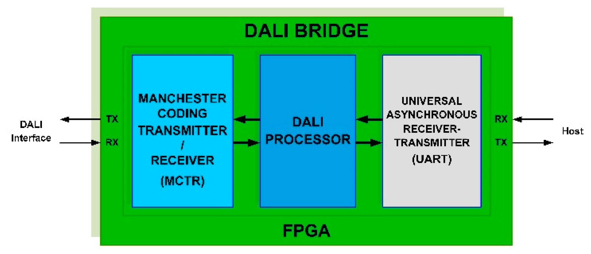
The DALI Bridge receives, interprets, and transmits DALI commands and information between two interfaces. The DALI Bridge has the purpose of decoding and encoding the data sent between the Host and the DALI Interface.
Figure 1 shows the schematic block diagram of the DALI Bridge connection.
The DALI Bridge design was based on the following criteria:
HW implementation for real-time execution.
Portable description developed in Very High-Speed Integrated Circuit (VHSIC) Hardware Description Language (HDL) (VHDL-93) that can be synthesized with any tool compatible with the IEEE Standard 1076-93.
The implementation in the FPGA will be conducted using only the LUTs (Look Up Tables).
Integration in FPGAs with low cost, low power consumption and with a reduced number of LUTs.
Flexibility to support upgrades and reconfiguration.
Development of a UART communication interface for easy connection to any device, peripheral or Wireless Sensor Node.
Support for the communication of street lighting applications in IoT.
The necessary aspects to apply the DALI Bridge in WSNs have also been taken into account, enabling the development of an integral and autonomous architecture, with scalability and adaptable power, and allowing a direct communication with other devices such as MCUs or “desktop computers”, without depending on external plugins. In short, the DALI Bridge handles all communications directly, which offloads the MCU from computational work, avoiding waiting for events and interruptions. Furthermore, the description of the DALI Bridge must be efficient in the use of the logic components of the FPGA since it must leave enough components free to allow the implementation of some additional processing algorithm.
3.2. Design Considerations for the DALI Bridge
This section begins by describing the DALI protocol, emphasizing the characteristics that make it difficult to implement by software and the section ends with an analysis of the communication protocol between the Bridge and the Host.
3.2.1. DALI Protocol
DALI is made up of a two-wire serial bus and requires a special power supply. It uses Manchester coding for the transmission and reception of data with a master/slave structure. The Master transmits 16 bits and the Slave (ballast) transmits 8 bits. The use of multiple masters is feasible, and a slave ballast can be shared by two masters. There are 64 channels or individual addresses for connecting ballasts to one interface line.
Manchester encoding is a digital signal format where the symbol “1” is represented by an ascending transition and the “0” is represented by a descending transition.
Figure 2 shows a DALI frame in which the temporal parameters related to the bit period, the signal transitions with respect to the logical values and the “bit transfer rate” are indicated.
The time period of both pulses (high and low) is half the bit period. The time of a bit is 833.33 μs. The transfer speed is 1200 bps with an acceptable error of ±10%. The packet sent by the control device to the receiver is called Forward frame and the response, Backward frame. In
Figure 3, it is shown that the Forward frame is 19-bits long and with the following order: 1 bit for “Start”, 8 bits for the address, 8 bits for the DALI command and 2 bits for “Stop”. Meanwhile, the Backward frame is 11-bits long and with the following order: 1 “Start” bit, 8 data bits, and 2 “Stop” bits. In both cases, the Most Significant Bit (MSB) is sent first.
Regarding the transmission time, the half-bit time is 416.67 μs. The slot timing range specifies the minimum (374.99 μs) and maximum (458.33 μs) time of the pulse at high and low levels. A Forward frame has a duration of 38 half bits, equivalent to 15.83 ms. A Backward frame takes 22 half bits or 9.17 ms. The time between two consecutive Forward frames is at least 22 half bits or 9.17 ms. The time between a Forward frame and a Backward frame is greater than or equal to 7 half-bit times or 2.92 ms, and less than or equal to 22 half-bit times or 9.17 ms. The time between a Backward frame and a consecutive Forward frame is at least 22 half bits or 9.17 ms.
Therefore, neither Manchester encoding/decoding, nor the DALI frame format can be implemented through a standard serial port of an MCU. To implement the DALI Bridge, a specific interface must be designed to fulfill the characteristics previously indicated. The interface could be implemented by software, using a General Purpose Input/Output (GPIO) port and the timers required to time all the events necessary for the transmission and reception of the frames, but, as indicated in the introduction, it may happen that the MCU does not have the sufficient processing capacity or resources to guarantee compliance with the bit timing, receive and transmit the frames, and perform the rest of the functions of a node in a WSN. Therefore, the need arises to develop a bridge that implements the DALI protocol and that controls the ballast according to the commands sent by the MCU of the WSN node. The characteristics of the communication between the bridge and the host of the wireless node are indicated in the following section.
3.2.2. Communication between the Host and the DALI Bridge
The DALI Bridge can be implemented within the WSN node itself, if the design is ad-hoc, or on another independent Printed Circuit Board (PCB). In both cases the communication will be through a standard asynchronous serial port. In this way, any device can act as a host, for example, an MCU, a Wireless System on a Chip (SoC) or a desktop computer. The serial port is configured by default at a speed of 9600 bps, 8 bits per character, even parity bit and one stop bit, but it can be synthesized with any other standard speed.
The DALI Bridge controls the operation of the ballasts by decoding commands. For this purpose, the Host sends commands to the DALI Bridge, which first decodes them and, depending on the type of command, executes them, sending the corresponding frames to the ballast. The data in the Request Frame that the host sends to the bridge consist of three fields, as indicated in
Figure 4. Each field is 11 bits in size, according to the asynchronous communication format indicated above. The first field is the command for the bridge, the second the address of the DALI device and the third the command information for that device. The return data from the ballast are sent by the bridge to the Host, in the format shown in
Figure 5. The format is divided into two fields, the acknowledgment, and the data, of a size of 1 byte. The acknowledgment indicates if valid data are returned from the ballast and that, therefore, the data are sent in the response.
There are general commands for the DALI Bridge and separate commands for DALI. Some of the implemented commands are indicated in
Table 1.
The command 00 (ECHO) allows the host to know if it has a bridge connected to its serial port. Command 01 is used to initialize the DALI Bridge components to a known state, for later commissioning. Command 02 is used to find out the status of the DALI Bridge. There are two bits to know its state. For example, the overload status bit determines the existence of a short circuit on the DALI bus for more than 254 ms, which allows the DALI Interface to be automatically deactivated. The other bit indicates whether the DALI Bridge has received the response after the execution of command 05, so if the data are not received, this bit is asserted. The set of DALI commands allow the control of the lighting, know the status, and configure the ballast. Command 04 is used to send DALI lighting control commands, such as those that control arc power. Command 05 is used to send DALI commands and to know the status of the ballast, for example, to determine if a ballast works, if it is on, and check the lighting level. Command 06 is used to send DALI ballast configuration commands, for example, to turn the ballast on, turn it off or reset it. Command 07 allows the identification of the DALI Bridge in the network.
When the command to check the status of the ballast is executed, a DALI Response (1 Byte) is received that allows verifying various ballast factors, based on the decoding of the bits, for example, when the least significant bit is zero, it indicates that the ballast is OK; if the next bit is active (1), it indicates that the lamp is burned out; if the bit in position two has the value zero, it indicates that the ballast is off, otherwise it is on; if the most significant bit is equal to zero, it indicates that the power supply is OK, otherwise there is no power supply, as indicated in
Table 2.
3.3. DALI Bridge Description FPGA-Based
As indicated in the introduction, the DALI Bridge was implemented in hardware by means of an FPGA, since in this way the operation is guaranteed, both from a logical and temporal point of view. One of the design objectives is to make a portable description, so that the bridge can be implemented in any FPGA of any manufacturer. For this reason, it was described using a Standard HDL, specifically through VHDL following the standard 1076-93.
The system was divided into three components: the UART, the DALI Processor, and the Manchester Coding Transmitter/Receiver (MCTR). The block diagram of the DALI Bridge is shown in
Figure 6. The operation of each component was described using a Finite State Machine with Embedded Data Path (FSMD). The DALI Bridge was designed as a completely synchronous system, so that all components use the same clock signal, and, in turn, their operating modes are synchronous. Only the asynchronous preset or clear inputs of the flip-flops are used to initialize them when the reset input of the DALI Bridge is activated. This ensures higher frequency operation by reducing clock signal skew problems in the FPGA and making it easier to place and route the design in the FPGA. The component entities were configured using a generic to specify the frequency of the clock signal, whose value depends on where the design is implemented. Based on this generic, the parameter values of the components that establish the different timings used in the DALI Bridge are determined. The three components that make up the DALI Bridge are described below.
3.3.1. UART
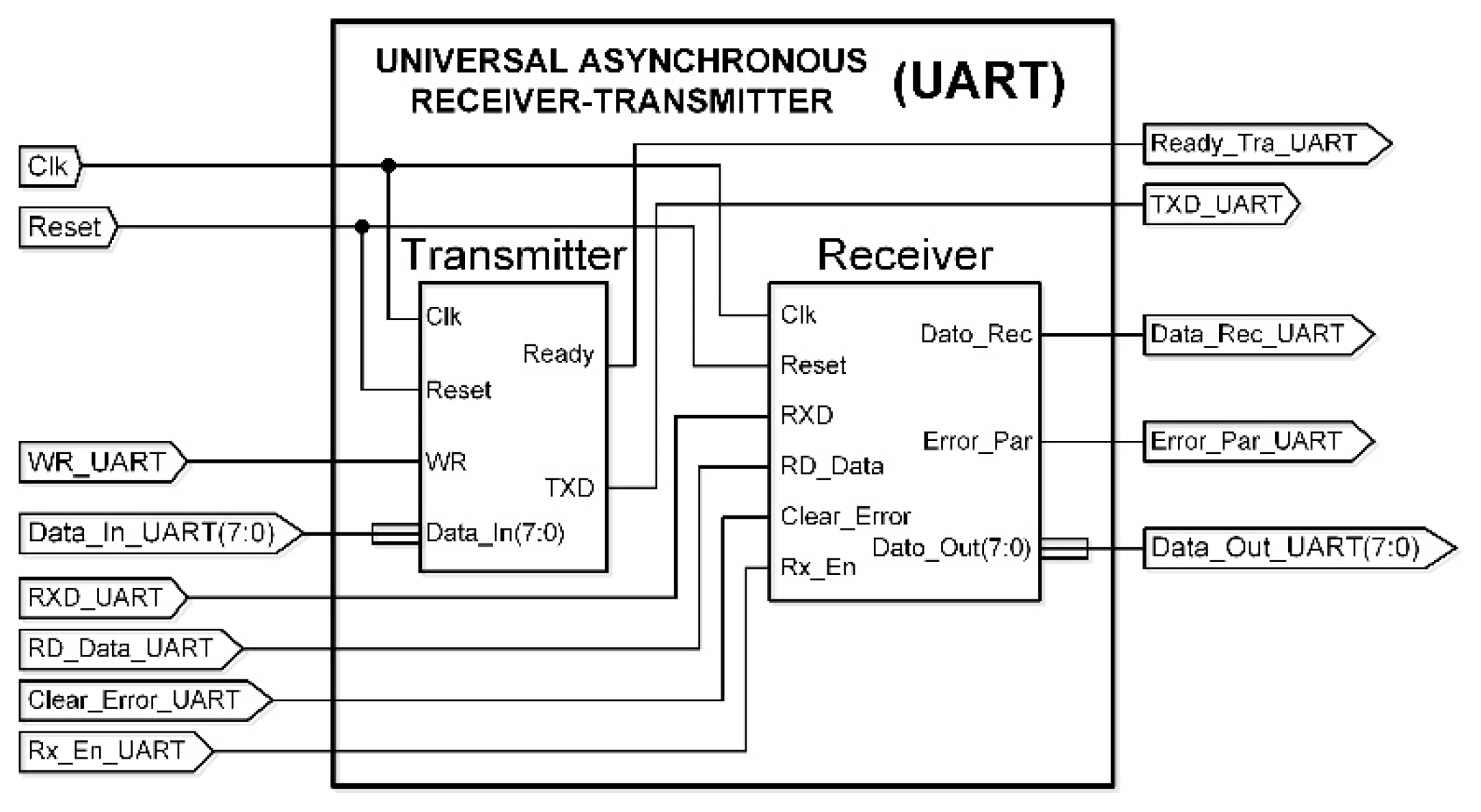
The entity in
Figure 7 corresponds to the UART. The function of the UART within the DALI Bridge is to carry out communication between the DALI Processor and the Host, transmitting and receiving data between both components. To fulfill these purposes, the UART has two components, the Transmitter, and the Receiver.
The UART was described so that any baud rate can be configured. By default, it is set to 9600 bits per second (104 µs per bit). The characters that are transmitted have a size of 11 bits with the format indicated in
Section 3.2.2. Transmission begins with the least significant bit. The ports of the UART that correspond specifically to the transmitter are: CLK, Reset, WR_UART, Data_In_UART (7:0), READY_Tra_UART and TXD_UART. The data path consists of four registers, which are: an input buffer register, a serializer register, a baud rate register, and a counter register. The buffer register performs the parallel load operation since its function is to store the character to be transmitted. The serializer register performs the parallel load and shift right operations to generate the parallel-to-serial conversion. This register has a size of 10 bits, since it must store the start bit (0), in the least significant position, the 8 bits to be transmitted and the even parity bit. The baud rate generator generates the clock signal that synchronizes the data transmission. The counter register counts the bits that are transmitted to determine the end of the transmission.
The description of the transmitter was made in an FSMD. The transmission process starts when the control unit detects that the WR_UART signal is activated, then the parallel data applied in Data_In_UART are loaded into the buffer register. The contents of the buffer register are then transferred to the serializer register and the baud generator register is initialized with zero. Once the character to be transmitted is stored in the serializer register, the count is enabled in the baud generator register. Every time the baud-generating register determines that the bit time has elapsed, a bit is transmitted through the TXD output, that is, a right shift is made in the serializer register by entering a 1 from the left. Obviously, the necessary shifts are subsequently made to transmit all the bits, for this, the counter is used, which increases its count, each time a bit is transmitted. By introducing a bit with value 1 in each shift, the stop bit is generated automatically after transmitting the previously stored 10 bits, thus saving a bit in the serializer register.
The UART ports that correspond specifically to the receiver are: CLK, Reset, RXD_UART, RD_Data_UART, Clear_Error_UART, Rx_En_UART, Data_Rec_UART, Error_Par_UART, and Data_Out_UART (7:0). The receiver should sample the receive input, RXD_UART, in roughly half the bit time to ensure correct reception. Therefore, sampling is performed at a frequency 16 times higher than the transmission frequency. The data path consists of an input buffer register, a data register, a frequency divider register, a baud rate generator, and a counter register. The buffer register stores the received character. The data register performs serial load and shift right operations to convert from serial to parallel. The frequency divider register generates a pulse type signal with a frequency 16 times higher than the transmission frequency to guarantee correct sampling of the receive input (RXD_UART), as indicated above. The baud rate generator, from the previous signal, activates its output to indicate the moment of capture of the received bit. The counter register counts the bits received to determine the end of data reception.
The data path and the receiver control unit were described by an FSMD. In the idle state, the baud generator register is initialized to zero and the counter register with the number of bits to receive. The reception process starts when the control unit detects that the Rx_En input is activated and the RXD_UART input has a zero value (start bit), then a time equivalent to half a bit is waited to correctly synchronize with the midpoint of the start bit. Once the reception is synchronized, a bit time is waited successively to sample the remaining bits at the midpoint of each one of them. The bit time is measured by the baud rate generator, so each time its output is activated, the received bit is stored in the RXD_UART input, making a right shift in the data register, and the counter register is decremented. At the same time, the value of the even parity of the received bits is updated. This process is repeated until the counter register is set to 0, indicating that all the bits have been received. Finally, the Data_Rec_UART signal is activated to indicate to the DALI Processor that data have been received. If a parity error has occurred, Error_Par is activated and is maintained until Clear_error is activated.
3.3.2. DALI Processor
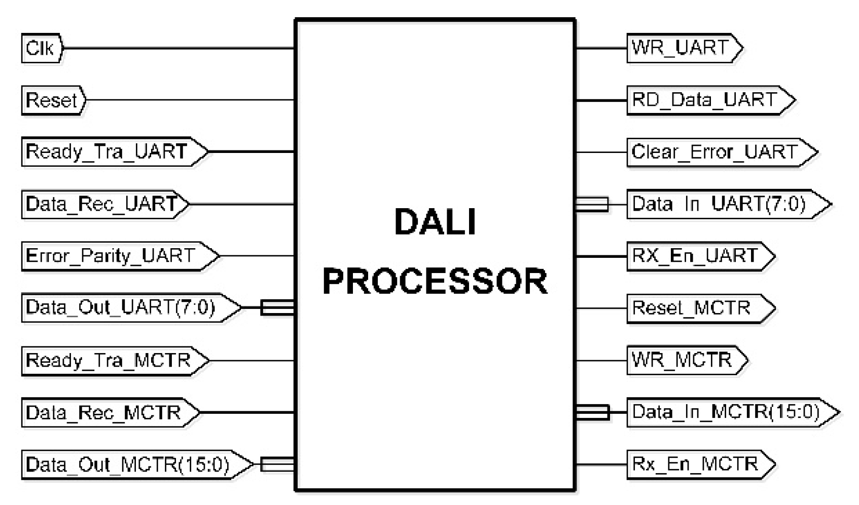
The DALI Processor entity aims to control the information exchange between the UART and MCTR entities. It performs the decoding of the DALI instructions and commands, which it receives from the host, and encodes the responses from the DALI Interface that it returns to the host. The DALI Processor Entity is shown in
Figure 8.
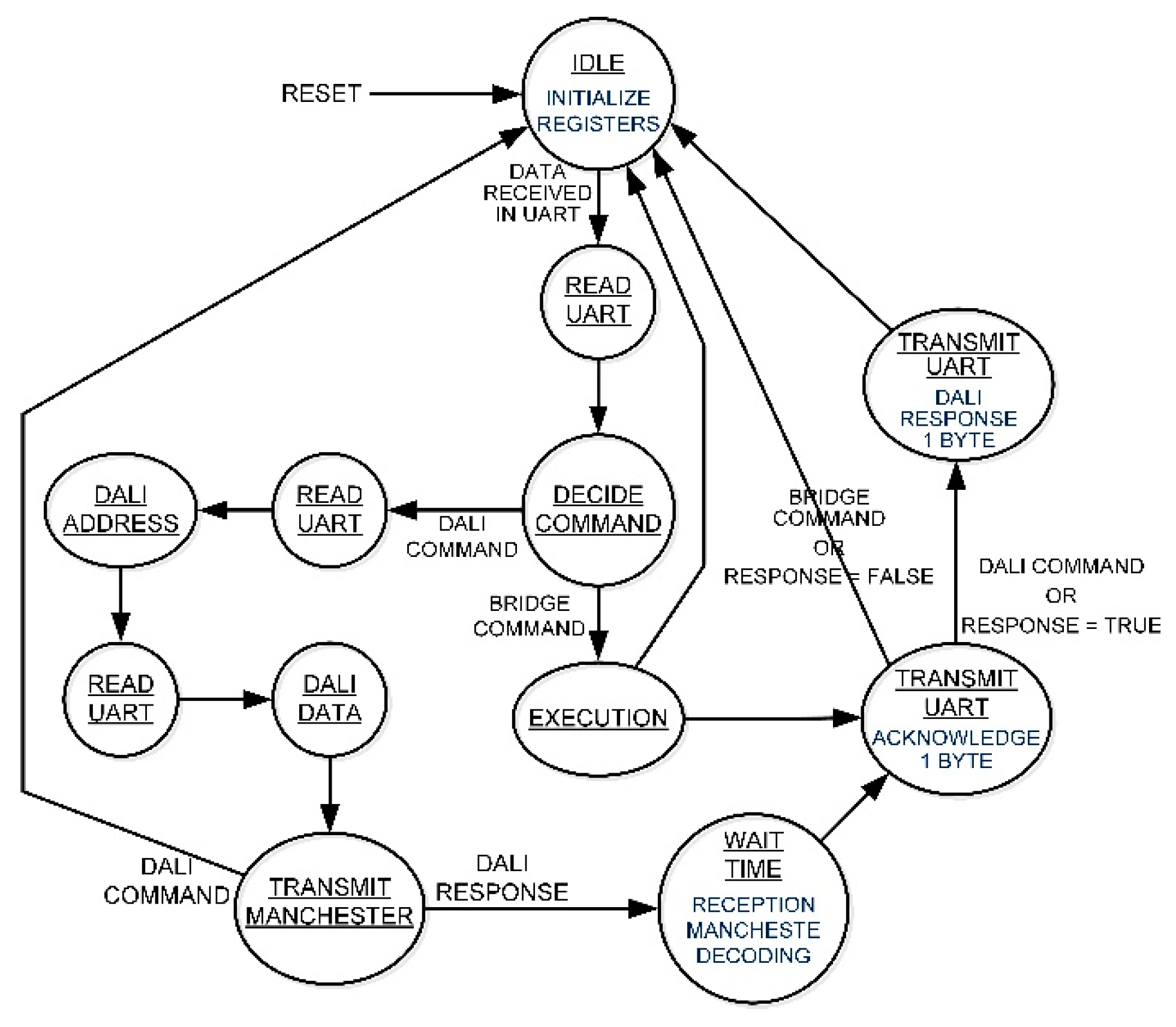
The description of the data path and the control unit of the DALI Processor was described by an FSMD, and its simplified state diagram is shown in
Figure 9. The data path consists of seven registers, which are: Instruction, Data_UART, Forward_MCTR, Backward_MCTR, Bridge_acknowledge, DALI_acknowledge and False_acknowledge. The Instruction register stores the command received by the UART. The UART_Data register stores the data that are transmitted to the UART. The Forward_MCTR register is 16 bits in size and is used to store the data that will be sent to the MCTR. The Backward_MCTR register stores the return data from the MCTR. The Bridge_acknowledge register stores the response from the execution of a Bridge Command. The DALI_acknowledge register stores the response from the execution of a DALI Command. The DALI_Response register stores the response data of the execution of a DALI Command.
In the FSMD start state all auxiliary and output signals are initialized. The command decoding process starts when the control unit detects that the Data_Rec_UART signal is active, at which time the data coming from the UART are read by the Data_Out_UART (7:0) input and stored in the Instruction register. The command is then interpreted to determine whether it is a command for the Bridge or a DALI command itself. In the case of a command for the Bridge, it is executed and, if a response is requested, the current parameters of the Bridge state are loaded into the Bridge_acknowledge register and, later, transferred to the Data_In_UART (7:0) output to send them to the UART.
3.3.3. MCTR
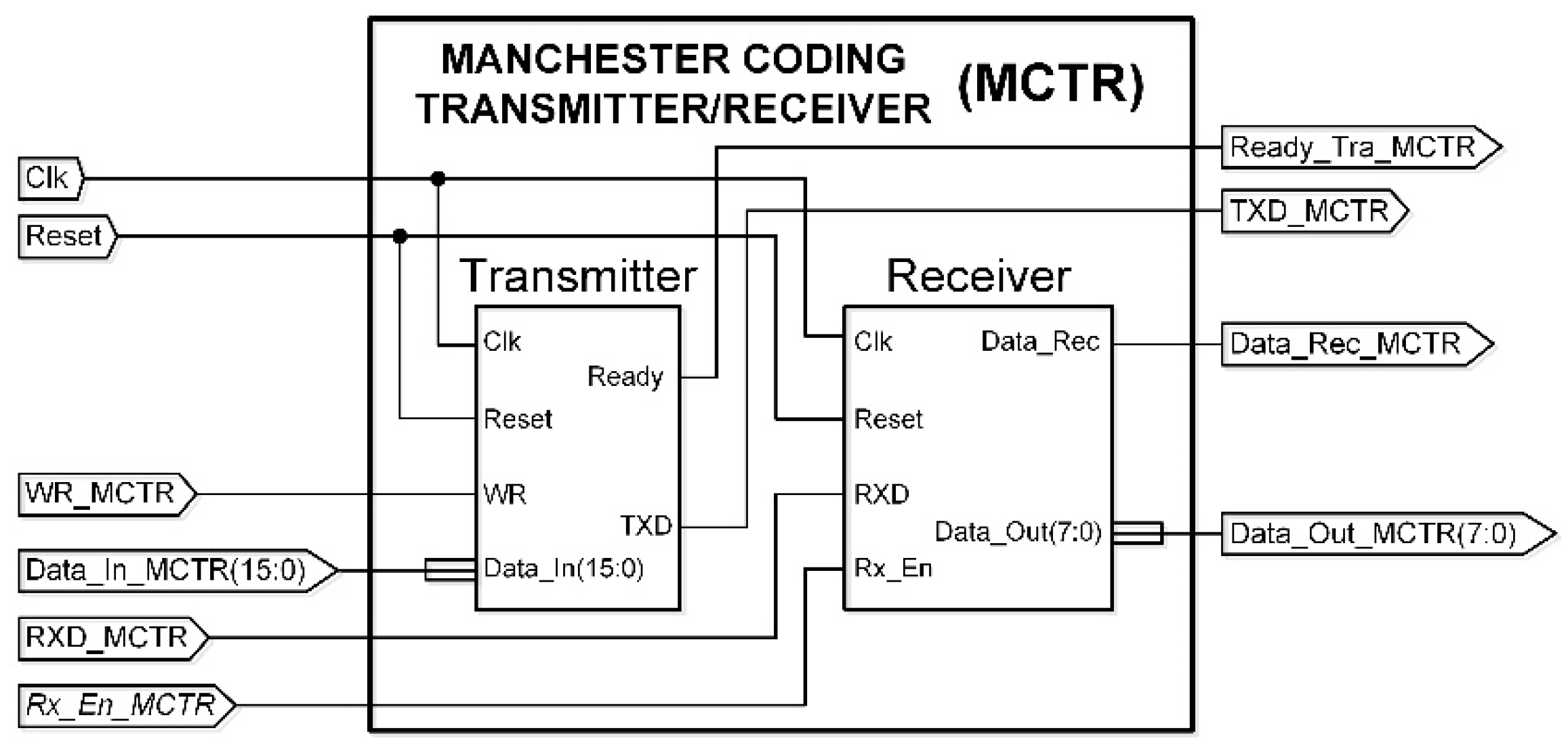
The function of the MCTR entity is to exchange data between the DALI Processor entity and the DALI Interface. The MCTR design was made with two blocks called Transmitter and Receiver, whose interconnection is shown in
Figure 10.
The MCTR entity transmits and receives Manchester encoded data, complying with the specifications indicated in
Section 3.2.2.
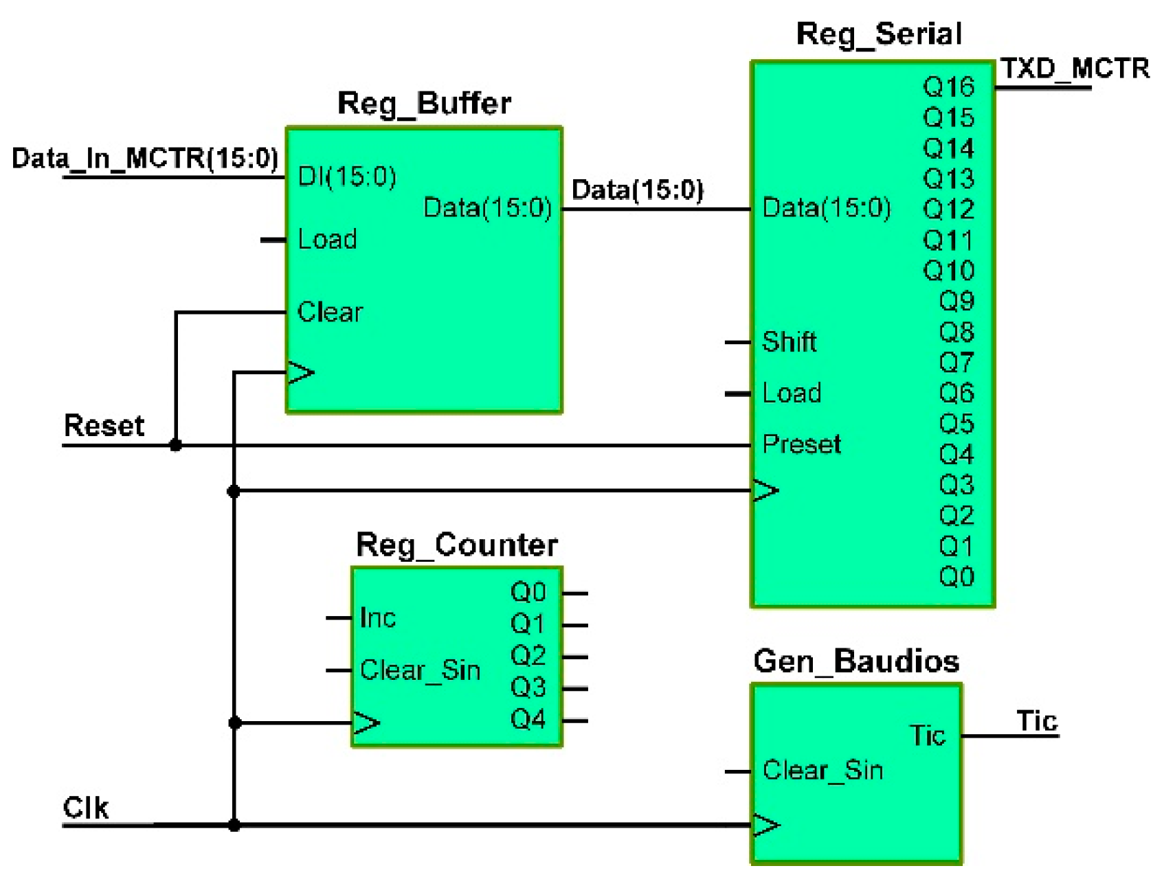
The MCTR ports that correspond specifically to the transmitter are: CLK, Reset, WR_MCTR, Data_In_MCTR (15:0), Ready_Tra_MCTR, and TXD_MCTR. The commands that are transmitted have a size of 19 bits. Transmission begins with the most significant bit. The MCTR transmitter data path is shown in
Figure 11. It consists of an input buffer register (Reg_buffer), a serializer register (Reg_serial), a baud generator register (Gen_baud) and a counter register (Reg_counter).
The buffer register performs the parallel load operation, and its function is to store the command to be transmitted. The serializer register has a size of 17 bits, since it must contain the start bit (1), in the most significant position, and the 16 bits to be transmitted. This register performs parallel load and shift left operations to convert from parallel to serial. The baud rate generator generates a pulse type signal (Tic) that is activated each time the half-bit timing is fulfilled, that is, every 416.67 µs. The counter register counts the bits that are transmitted to determine the end of the transmission. The data path and control unit of the transmitter was described by an FSMD.
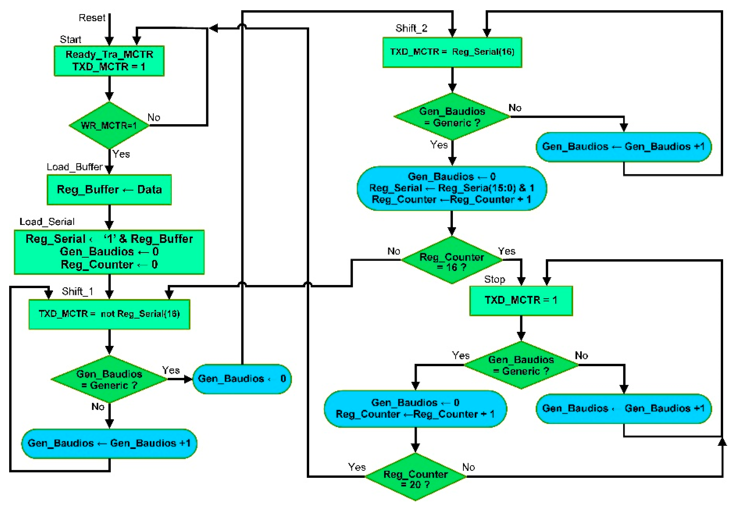
The Algorithmic State Machine (ASM) diagram of the MCTR transmitter control unit is shown in
Figure 12. In the Start state, Ready_Tra_MCTR is activated to indicate to the DALI Processor that it is not transmitting and therefore that it can write a command to transmit it to the DALI Interface. The transmission process starts when the control unit detects that the write input, WR_MCTR, is activated. If so, the parallel data to be transmitted are loaded into the buffer register and wait for WR_MCTR to be deactivated. Once writing is deactivated, the Load_serial state is transferred, in which the contents of the buffer register are transferred to the serializer register, and the baud generator register and the counter register are initialized to zero. The Shift1 and Shift2 states perform the transmission of a bit in the Manchester code. To do this, in the Shift1 state the first half bit, which is the complement of the value of the data bit, is transmitted through the TXD_MCTR output, and in the Shift2 state the second half bit, which is the value of the bit. In this way, the corresponding transition is generated according to the Manchester encoding described in
Section 3.2.2. In both states, time counting is enabled in the baud generator register to count the number of pulses equivalent to the half-bit time (416.67 μs), and if it reaches its final count, it is initialized to zero. In the Shift1 state, you simply go to the Shift2 state, once the first half bit has been transmitted. In the Shift2 state, the serial register is shifted one bit to the left and the counter register is increased each time the baud generator activates a Tic. This sequence is repeated until all data bits have been transmitted, so the value of the counter register must be checked. If this has reached 16, it goes to the Stop state, to transmit the two stop bits, otherwise it returns to the Shift1 state. In the Stop state, the transmit output is set to 1 for four half bits to terminate the transmission of the forward frame. For this reason, the baud generator register count is enabled, and each time it reaches its final count it is initialized to zero, and the counter register is increased. This process is repeated until the counter register has the value 20, which indicates that all the bits have already been transmitted, so it returns to the Start state, in which the transmission output is set to 1, which corresponds to the idle status.
The receiver specifically corresponds to the following MCTR ports: CLK, Reset, RXD_MCTR, Rx_En_MCTR, Data_Rec_MCTR and Data_Out_MCTR (7:0). The receiver receives the Backward frames, which consist of 11 bits. To ensure that the reception is correct, the receiver performs the sampling of the information at the midpoint of each first half bit, as shown in
Figure 13. In doing so, the decoding of the received Manchester data is performed at the same time, since the value of each bit will be the complement of the value read in the reception input. To synchronize with the midpoint of the pulse at the low level of the start bit, the initial transition is detected, and a quarter of the bit time is waited, that is, 208.33 μs. Once the reception has been synchronized, to receive the rest of the bits, only the reception input must be sampled each bit time. To count these times with good precision, a clock with a frequency 32 times higher than that of reception will be used as the time base.
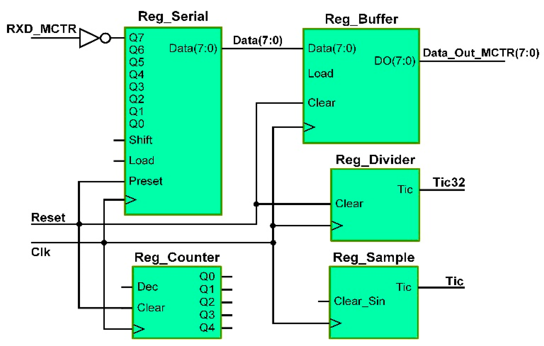
The MCTR receiver data path is shown in
Figure 14. It consists of an input buffer register (Reg_Buffer), a serial register (Reg_Serial), a frequency divider register (Reg_Serial), a sampling register (Reg_Sample) and a counter register (Reg_Counter). The buffer register stores the received data. The serial register performs serial load and shift left operations to generate the serial-to-parallel conversion. The frequency divider register generates the clock signal (Tic32) that is used as a time base to synchronize the reception. The sample register determines the moment of capture of the bit received from Tic32. The counter register counts the bits that are received.
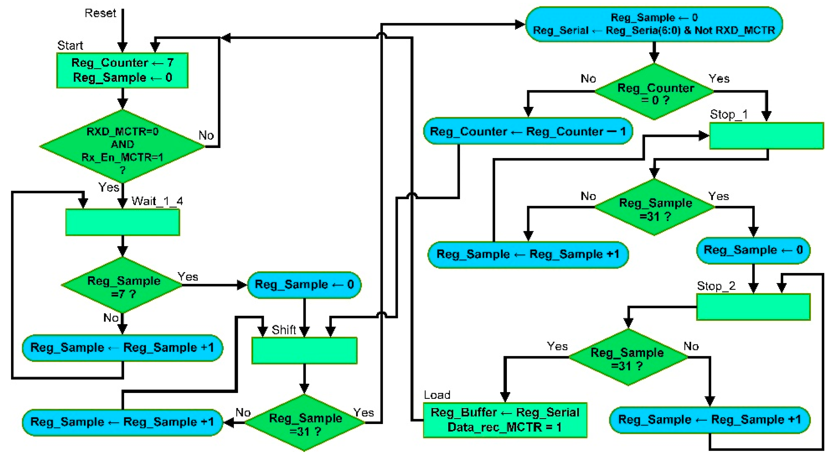
The description of the receiver was made by means of an FSMD, whose ASM diagram of the control unit is shown in
Figure 15. In the Start state, the baud generator register is initialized with zero and the counter register with the appropriate value to detect the end of the reception of the data bits. In this state it is expected to receive the start bit to begin the reception process. This starts if the reception enable input, Rx_En_MCTR, is active and the data reception input, RXD_MCTR, has the value 0 (start bit). If this double condition is met, the process indicated above is carried out, which can be seen in the ASM diagram of the FSMD. It goes to the Wait_1_4 state in which a quarter of the bit time is waited to synchronize with the start bit. To time this, the sampling register is used, which is incremented each time Tic32 is activated. If the sampling register reaches count 7, it is initialized with the value 0 and goes to the Shift state to receive the eight data bits. As already indicated, a bit time must be waited and the complement of the value of the receive input must be loaded serially into the serial register. To do this, each time the sampling register reaches the value 31, a shift to the left is made in the serial register, loading the complement of the value of the reception input, and the counter register is decremented. This sequence is repeated in the Shift state until the counter register reaches the zero count, which indicates that it only remains to receive the two stop bits. To do this, the Stop_1 and Stop_2 states are used, in each of which a bit time is waited to validate them, and the Load state is entered in which the content of the serial register is transferred to the reception buffer, and the Output signal Data_rec_MCTR is activated to indicate the DALI Processor that a Backward frame has just been received from the DALI interface.
3.4. Implementation of the DALI Bridge in a Wireless Sensor Node for IoT
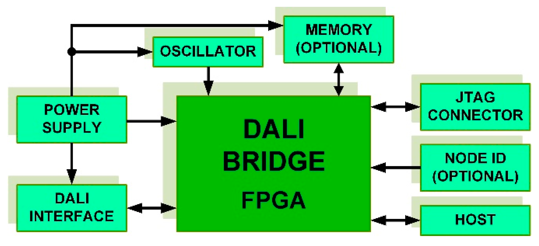
The implementation of the DALI Bridge in an FPGA embedded in a wireless sensor node requires a set of basic elements that are shown in the block diagram of
Figure 16, where the FPGA is distinguished as the key element, in addition to an oscillator circuit, a Joint Test Action Group (JTAG) Connector, the DALI Interface, a Power Supply circuit and optionally a memory and a Node ID.
The main element to implement the DALI Bridge is the FPGA, which has certain basic characteristics without the need for specific blocks, such as being ultra-low power consumption or low cost and, therefore, with a reduced number of logic resources. On the other hand, it may be desirable to have the ability to dynamically disable Phase Locked Loops (PLLs) to decrease static and dynamic power consumption. Currently, all low-cost FPGAs include specific function blocks, such as Block Random Access Memory (BRAM) and Digital Signal Processing (DSP). None of these blocks are necessary in this design, but they could be used, especially RAM blocks, in future versions to improve performance, such as including a First-In, First-Out (FIFO) memory in each of the receivers. The FPGA must allow different configuration methods such as: Master SPI, Slave SPI, Non-Volatile Configuration Memory (NVCM) and JTAG.
Obviously, if the FPGA is volatile in nature, as it is not powered, the DALI Bridge configuration stored inside will be lost. To avoid this problem, an external memory must be used to store the configuration data, so that in the power-up, the FPGA itself transfers the contents of the external memory to its internal configuration memory. The most common element used to achieve this is an SPI series FLASH memory due to its low cost. This external memory must comply with the compatibility restrictions presented by the FPGA, which are mainly: the supply and operating voltage range, as well as the support for operations in the frequency range of the FPGA’s internal oscillator. It must also meet the necessary requirements for communication through the serial or parallel port of the FPGA that is used for its configuration.
Another basic element is the DALI Interface, which is essential to adapt the logic voltage levels between the DALI Bridge and the ballast. The control of the DALI Interface must comply with the variable logic levels that depend on the operation of the ballast [
15]. For the high logic level, when the ballast is a receiver, the range is 9.5 V to 22.5 V, and when it is a transmitter the range is 11.5 V to 20.5 V. Otherwise, for the low logic level, when the ballast is a receiver, voltage levels vary from −6.5 V to +6.5 V, and when it is a transmitter they range from −4.5 V to +4.5 V. On the other hand, it must have an adequate communication range and the necessary electrical isolation with the other basic components. It is vital that the DALI Interface is compatible with the logic levels of the FPGA being used.
All the components of the DALI Bridge need a 3.3 VDC power supply to work, so the power supply unit will consist of an AC/DC converter. This converter must have an output voltage of 3.3 VDC, and its maximum output current will be limited by the type of host used, since, as indicated in the results section, the power consumption of the DALI Bridge is lower than 15 mW. Current FPGAs usually need several supply voltages; specifically, the Input/Output (I/O) blocks usually use a voltage of 3.3 VDC, but for the operation of their internal core they use a lower voltage, generally on the order of 1.2 VDC. On the other hand, they also usually need a different tension for their programming, which is usually an intermediate tension between the two previous ones. These two supply voltages inherent to the FPGA can be obtained using two Low Dropout (LDO) linear regulators, given the low power consumption of the bridge, but a switching regulator with double output could also be used. To supply the DALI Interface, although it is not the objective of this work, an isolated DC/DC converter can be used, which generates the necessary voltage from 3.3 VDC to be able to generate the logic levels of the DALI bus.
The FPGA needs a device to generate the clock signal, and the device in charge of performing this function is the oscillator. A precision oscillator with a programmable frequency range can be used as long as it allows one to generate several operating frequencies to have versatility in the wireless sensor node, in addition to allowing one to reduce power consumption according to the requirements that are demanded.
The JTAG connector is used for the FPGA configuration. This must comply with the IEEE 1149.1 standard, but in turn will have to adapt to the recommendations of the FPGA manufacturer. This connector has been included because it is usually the most common method, but the final solution will depend on the configuration options that the FPGA allows. If the system being designed has a USB connector, a USB-JTAG adapter could also be used. Regardless of the option chosen, if non-volatile memory is required, it must also allow its configuration.
Optionally, a Node ID selector can be included, which is the response value that is returned to the Host when command 04 is executed and serves as an identifier, both for the Bridge and as an identifier for the wireless sensor node in the network.
4. Results
This section presents the experimental results of the implementation of DALI Bridge in the FPGA embedded in a Wireless Sensor Node for IoT. The node where the DALI Bridge was integrated was developed to improve the “UCODALI” node which was described in detail in [
16]. In the UCODALI node, the DALI protocol was carried out by software in the SoC, which also had to perform the processing and wireless connection functions. This software implementation of the DALI protocol consumes two timers of the MCU hardware and forces the use of low-level functions of the operating system. The use of these types of functions complicates the application excessively and requires a careful analysis of the execution time to be able to comply with the time requirements of the DALI protocol. For these and other reasons, which have been discussed throughout this work, it was decided to free the SoC from the implementation of the DALI protocol, which motivated the development of the DALI Bridge and the new UCODALIB node.
4.1. Wireless Sensor Node Description of UCODALIB
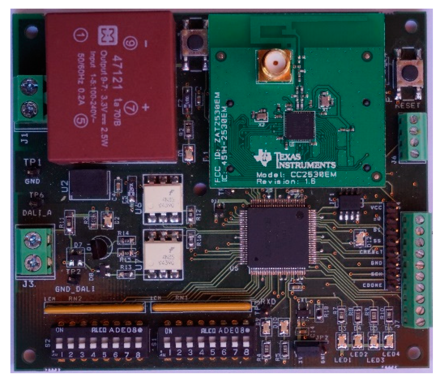
Figure 17 shows a photograph of the new UCODALIB node, which has the advantage of having all the necessary hardware elements for the implementation of the bridge and the DALI Interface integrated on a single PCB. The processing element is not integrated on the same PCB, but a generic connector has been dedicated to enable the connection of any MCU or SoC.
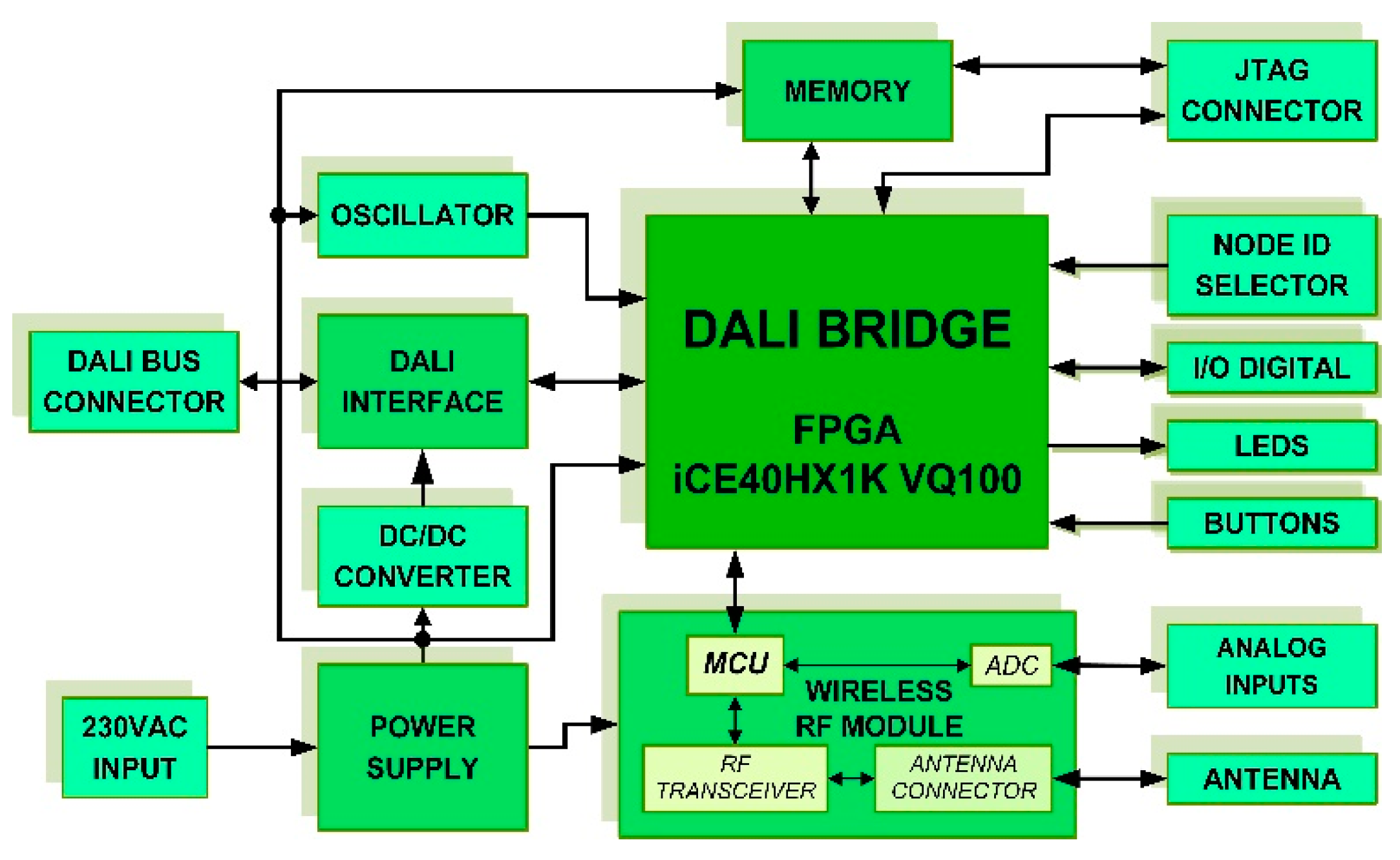
Figure 18 shows a block diagram that highlights the use of an FPGA to synthesize the bridge described in this work. In this figure, the following blocks are observed:
FPGA.
Serial Flash-Embedded Memory (SFEM).
DALI electrical interface.
Connector for the MCU.
Power Supply.
Node ID Selector and HMI (Human Machine Interface—buttons and LED).
The FPGA is the key component, where the functions for the DALI Bridge implementation were carried out, in addition to some interfaces to peripherals. The DALI Bridge was implemented in the Lattice Semiconductor FPGA iCE40HX1K-VQ100 [
41]. It is a low-cost, low-power FPGA that makes it ideal for use in the implementation of wireless sensor nodes. This FPGA offers limited resources based on Look-Up Tables (LUTs), Embedded Block RAM (EBR), NVCM and PLLs. It features programmable low-oscillation differential I/Os with the ability to dynamically disable on-chip PLLs to decrease static and dynamic power consumption. This FPGA is of the reprogrammable Static Random Access Memory (SRAM) type and supports different configuration modes: Master SPI, Slave SPI and NVCM.
Table 3 summarizes the logic resources of the FPGA.
The DALI Interface block adapts the logic voltage levels of the FPGA to those of the DALI bus, in addition to isolating the bus from the rest of the components on the board. A detailed description of this block can be found in [
16]. The M25P40VP Serial Flash Embedded Memory (SFEM) [
42] with capacity of 4 Mbytes has been chosen to store the description of the DALI Bridge and configure the FPGA through the SPI bus that connects the two circuits. For the initial configuration of the FPGA and SFEM, a JTAG connector is used. For the operation of the FPGA, the configurable precision oscillator LTC1799 [
43] has been used, which allows generating the clock signal with three frequency options: 33.3 MHz, 3.33 MHz and 0.333 Mhz. In this way, the most suitable frequency can be selected to achieve the lowest power consumption of the node.
The PCB has a slot made up of two connectors for inserting the wireless communication and processing module. Currently the SoC CC2530EM Module is used, which includes an MCU based on an enhanced version of the 8051 and RF components for wireless connection [
44].
By configuring two microswitches, the 16-bit size node identifier (Node ID) is set. The board has LEDs to visually monitor communications, general-purpose LEDs and two push buttons, one for reset and one for general purpose.
The supply of the different components of the Wireless Sensor Node UCODALIB is carried out with the FC47121 switching Power Supply [
45], since the voltage is obtained from the 230 VAC network. The FC47121 is based on flyback topology, making it ideal for low power applications. On the other hand, the hybrid module MEU1S0315ZC [
46] has been used to generate a supply voltage of 15 VDC for the DALI Interface, so that it can generate the appropriate voltage levels to control the ballast. This module is a DC/DC converter with galvanic isolation and a remarkably high efficiency.
4.2. Results of the Implementation of the DALI Bridge in the Wireless Sensor Node
The results of the bridge design synthesis are shown below in terms of logical resources used, bridge latency, estimated power consumption, and DALI interface bit time. The synthesis was performed for the FPGA iCE40HX1K-VQ100 using the iCEcube2 tool from Lattice Semiconductor [
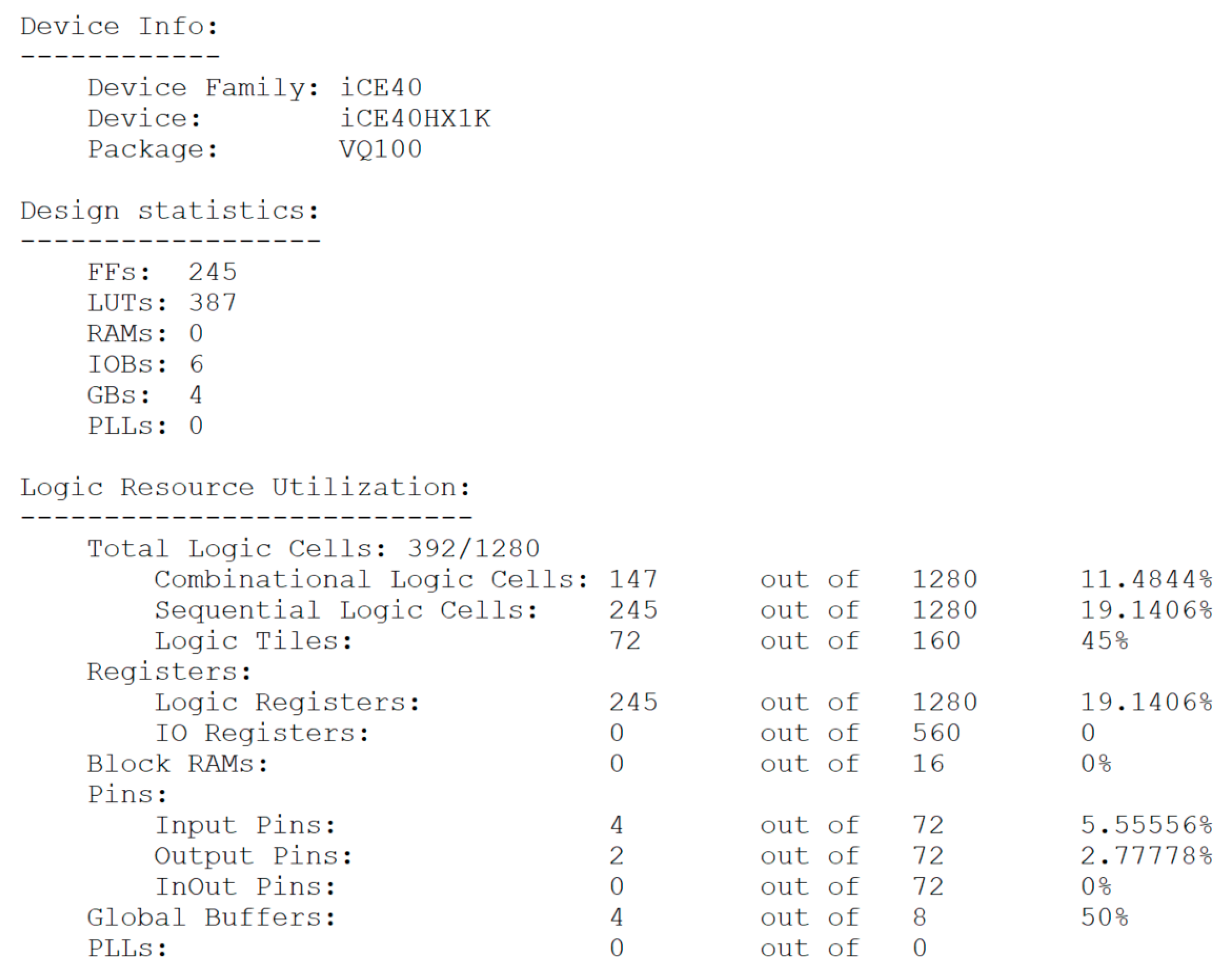
47]. A portable VHDL description of the Bridge has been made, seeking to minimize the consumption of logical resources, so that approximately 80% of LCs (Logic Cells) and 90% of the routing resources remain free. On the other hand, it does not use any of the RAM Blocks of the FPGA, which will be left free to improve the functionality of the bridge to implement other interfaces. This can be seen in
Figure 19 and
Figure 20.
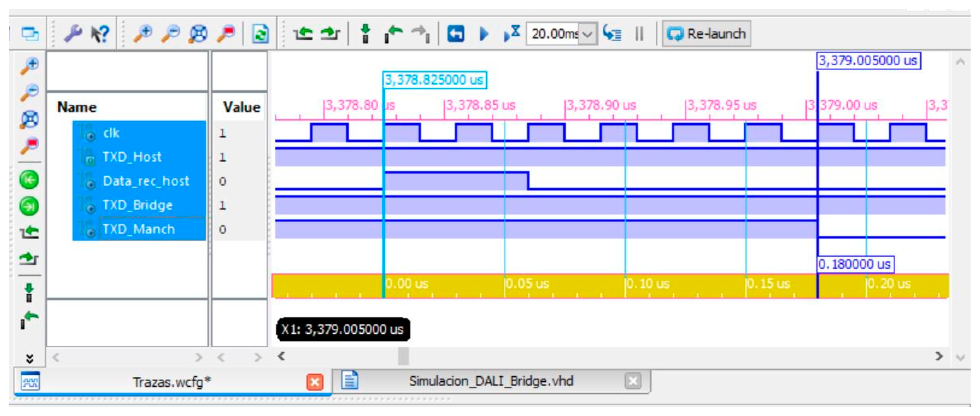
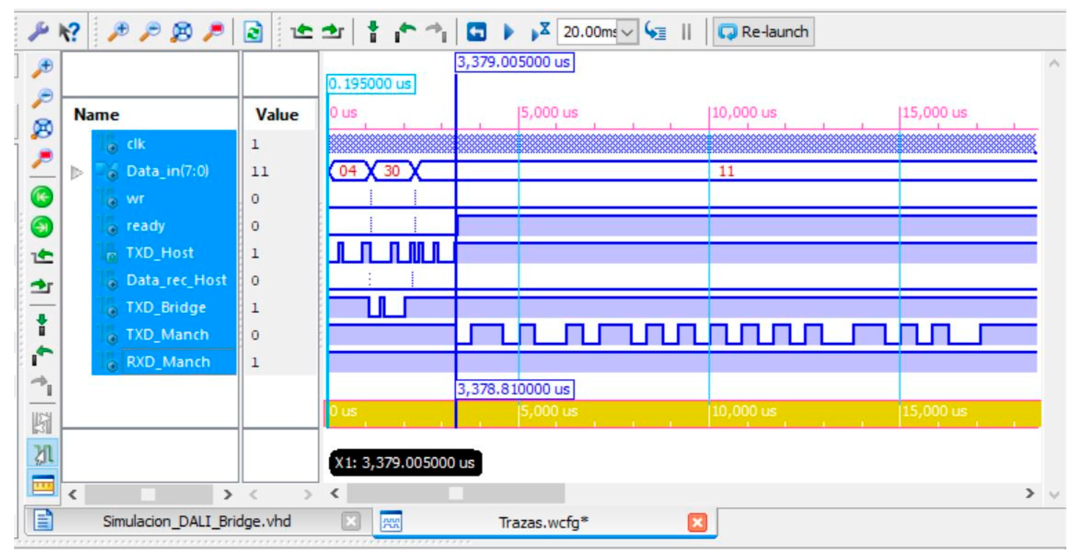
A particularly important parameter in any bridge design is the latency time. It is true that the data flow through the bridge is quite small and that the speeds of the interfaces on both sides are very low, so the latency time is not going to cause the bridge to malfunction. However, minimizing latency time is important so as not to add unnecessary delays. To measure the latency time, the execution of the DALI command number 04 of
Table 2 has been simulated, operating at a frequency of 33.3 MHz. To do this, the time that elapses since it finishes receiving the command from the host and starts sending it to the DALI bus has been measured. This time is very small, specifically 180 ns, as can be seen in
Figure 21. On the other hand, the time from when the host sends the command to the Bridge and it responds by sending the frame to the DALI bus has also been measured. This has a value of 3.38 ms, as indicated in
Figure 22.
It should be noted that the last measured latency time is determined by the transmission speed, which in this case is 9600 bps, so it can be easily reduced, since the DALI Bridge can be configured with the highest speeds allowed by the MCUs.
Timing analysis was performed on the DALI Bridge synthesis to obtain the Clock Frequency, which is shown in
Figure 23. Regarding internal operations in the FPGA, it is observed that the implementation supports a target operating frequency of 122.40 MHz. In the calculation, the synthesizer takes into account the operating frequency of all individual logic resources (I/O Cells, LUTs, Flip-Flops and BRAM), the switching frequencies of the flip-flops of the logic cells and the delays of the combinational logic cells (LUT). If additional and independent modules are needed, which require operating at higher frequencies, it is possible to develop them on the same FPGA.
Table 4 shows the breakdown of the estimated power dissipation as a function of frequency and temperature. The estimation was made for a supply voltage of the I/O banks of 3.3 V, since these are configured with the LVCMOS33 standard, and a supply voltage of the Core of 1.2 V. For the frequency values, three cases have been considered: the maximum operating frequency determined by the synthesis tool (122.40 MHz), and the two frequencies of the precision configurable oscillator, which has been used in the implementation of the wireless node (33.3 MHz and 3.33 MHz). From the data in the table it can be deduced that the power consumption in static mode is practically negligible, since in the most unfavorable condition (70 °C) it is only 1.41 mW. On the other hand, the power consumption in dynamic mode does not vary with temperature, and logically only depends on the frequency. Therefore, the total power consumption remains very stable over the entire temperature range (0 to 70 °C), varying only 1.1 mW.
Regarding the variation of power consumption with respect to frequency, there is a significant relative difference of 16.57 mW, between the maximum frequency (122.40 MHz) and the minimum frequency (3.33 MHz) at which the design could operate. Another conclusion that can be drawn is that if only the two frequencies of the oscillator mounted on the PCB are used, the absolute difference is only 4.88 mW. Therefore, if the FPGA were to perform some processing for which it had to operate at 33.3 MHz, the total power consumption would not be excessively increased.
This very low power consumption of the DALI Bridge considerably reduces the consumption of the UCODALIB node compared to that of the UCODALI node, since, as the SoC MCU has to perform less processing, it can operate at a lower frequency.
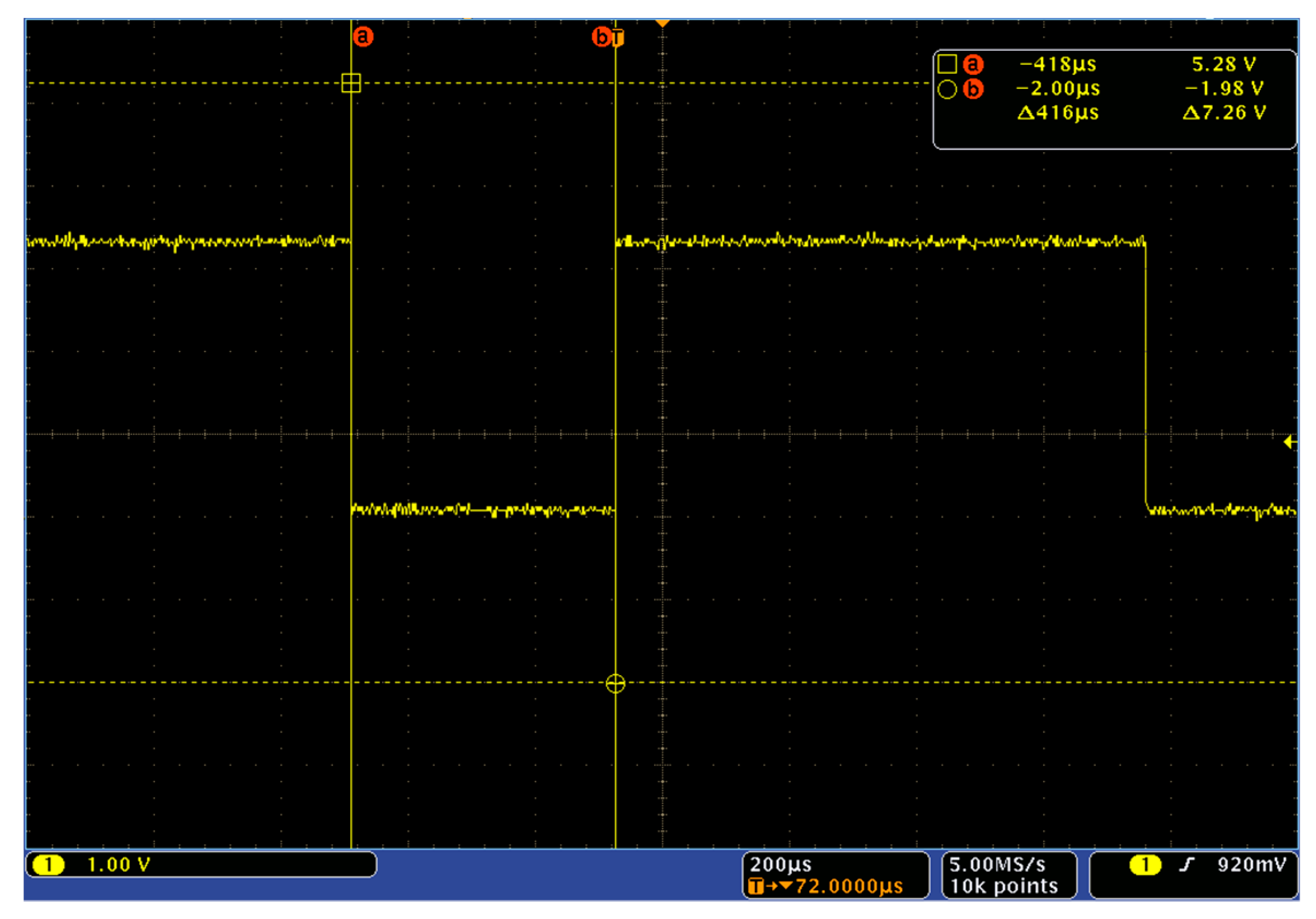
Another important point of the DALI protocol specifications is the bit time. Experimentally, the “bit transfer rate” was analyzed, where the mean time per bit (
Te) of 416 μs was obtained, and one-bit time of 832 μs, having only 0.16% error, a value within the error tolerance range allowed (10%), since the standard specifies that the one bit time must be 833.33 μs and therefore the average time per bit (
Te) must be 416.67 μs. This is shown in
Figure 24.
5. Conclusions
This work shows the description and implementation of the hardware DALI protocol in a low-cost, ultra-low power consumption FPGA, making it ideal for IoT applications in Smart Lighting systems. The choice of hardware implementation of the DALI protocol, creating a bridge between the DALI bus and the MCU, ensures the timing required for the bus bits, Manchester encoding and frame formatting. In addition, the bridge frees the application running on the MCU from the tedious task of composing the sent frames and performing Manchester encoding/decoding and timing. A reliable implementation of the DALI protocol is achieved regardless of the application, operating system, and timers available in the MCU and with a bit time precision unattainable with a software implementation.
The DALI Bridge has been developed to improve one of the wireless sensor nodes used in previous Smart Lighting systems applications, and in which the correct communication with the ballasts has been verified. This has meant an important simplification of the Application Programming Interface (API) that controls the ballasts and, therefore, also of the final application.
The DALI Bridge has been described according to the VHDL-93 standard, using the high-level descriptive resources of VHDL, for which a portable description has been obtained, that can be synthesized by all synthesis tools. Therefore, it can be implemented in any FPGA from any manufacturer. On the other hand, the description has been optimized to use the least possible number of logical resources which, in turn, are only those that all low-cost FPGAs have, such as LUTs, flip-flops and those necessary to implement arithmetic circuits, such as adders and counters.
In addition, in this work it has been shown that FPGAs are not only suitable for performing high performance computing tasks in wireless nodes and IoT, but also they are a good choice to implement control protocols, buses and interfaces to peripherals, due to their flexibility, and their low cost and power consumption.
Furthermore, the free space of logic resources of the FPGA allows for enough logic capacity to create modules for processing, algorithms, communication, or control of other sensors and/or actuators, independently of the DALI Bridge. All this makes use of FPGA’s decisiveness in WSNs.
The reduced number of logic resources used for the implementation of the DALI protocol in the FPGA allows the addition of another Bus Bit Error Control Module (B-BCoM). This module simultaneously reads the bits that it writes to the bus and compares them. In this way, at a physical level, bit errors that are very difficult or almost impossible to detect by a software-based DALI transmitter—since the comparison must be made in bit time—now can indeed be detected. This new module will allow us to detect short circuits, inadequate voltage values and drifts to ground.


