10 Clock-Periods Pipelined Implementation of AES-128 Encryption-Decryption Algorithm up to 28 Gbit/s Real Throughput by Xilinx Zynq UltraScale+ MPSoC ZCU102 Platform

 ,
, 
 and
and 
Abstract
1. Introduction
2. Materials and Methods
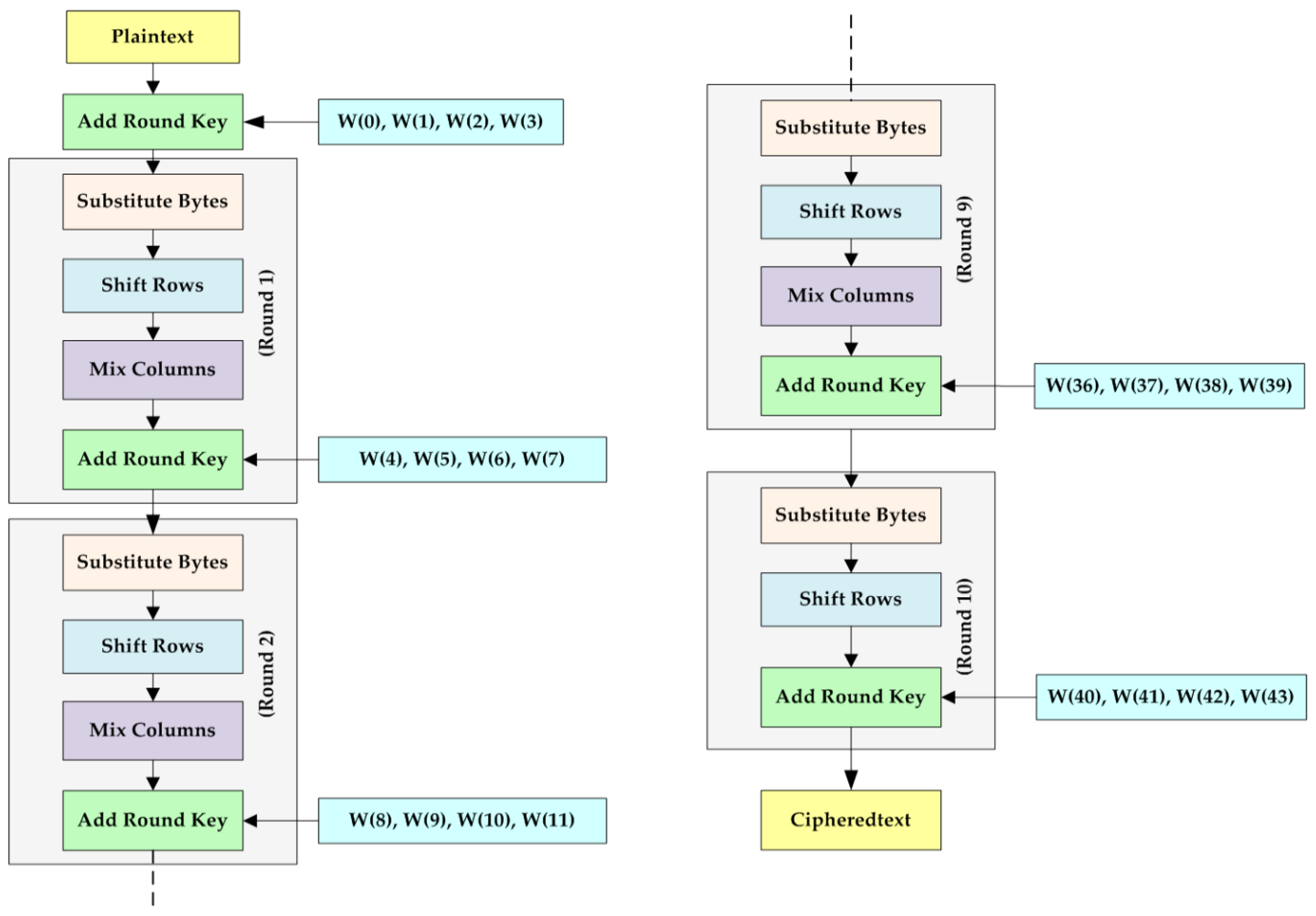
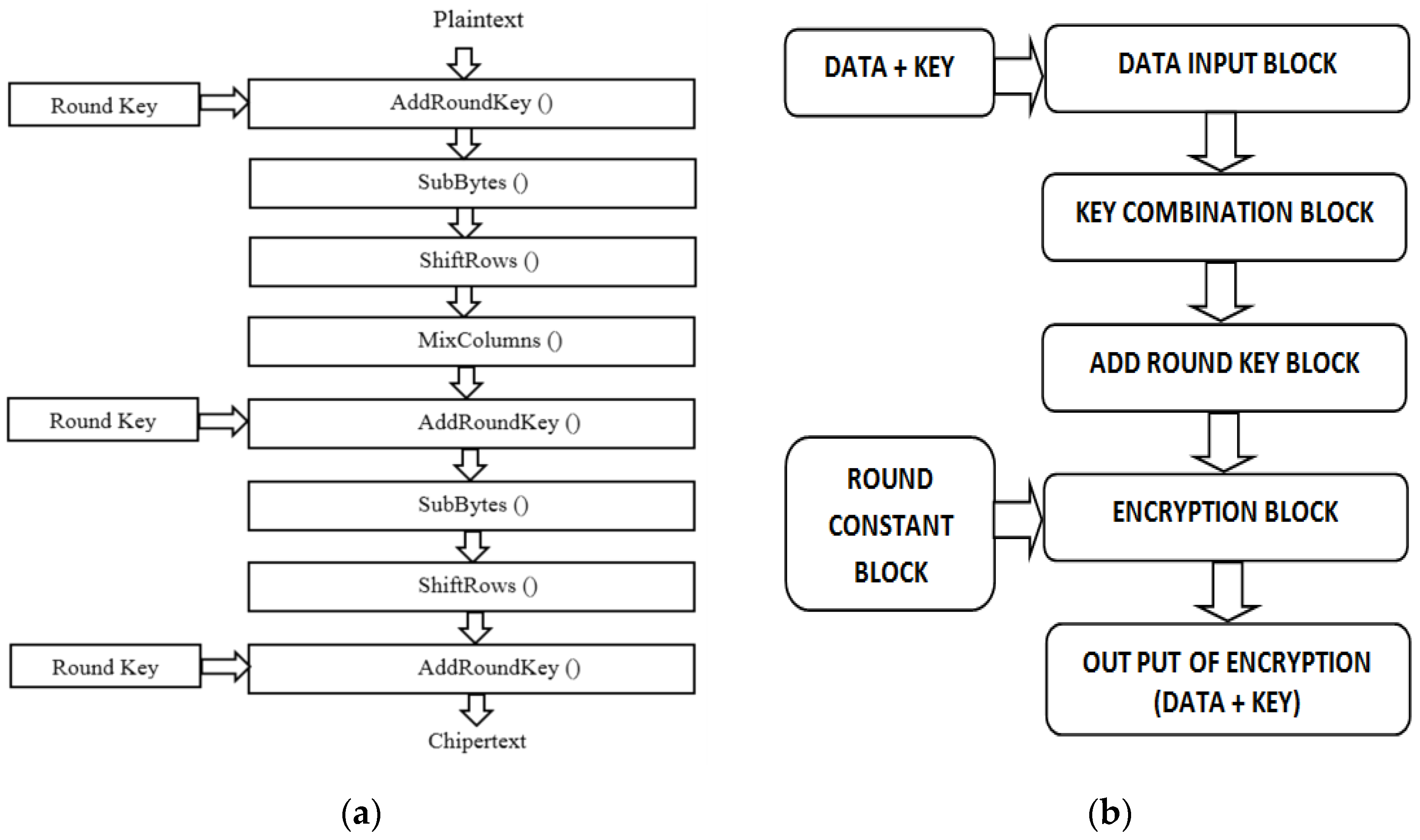
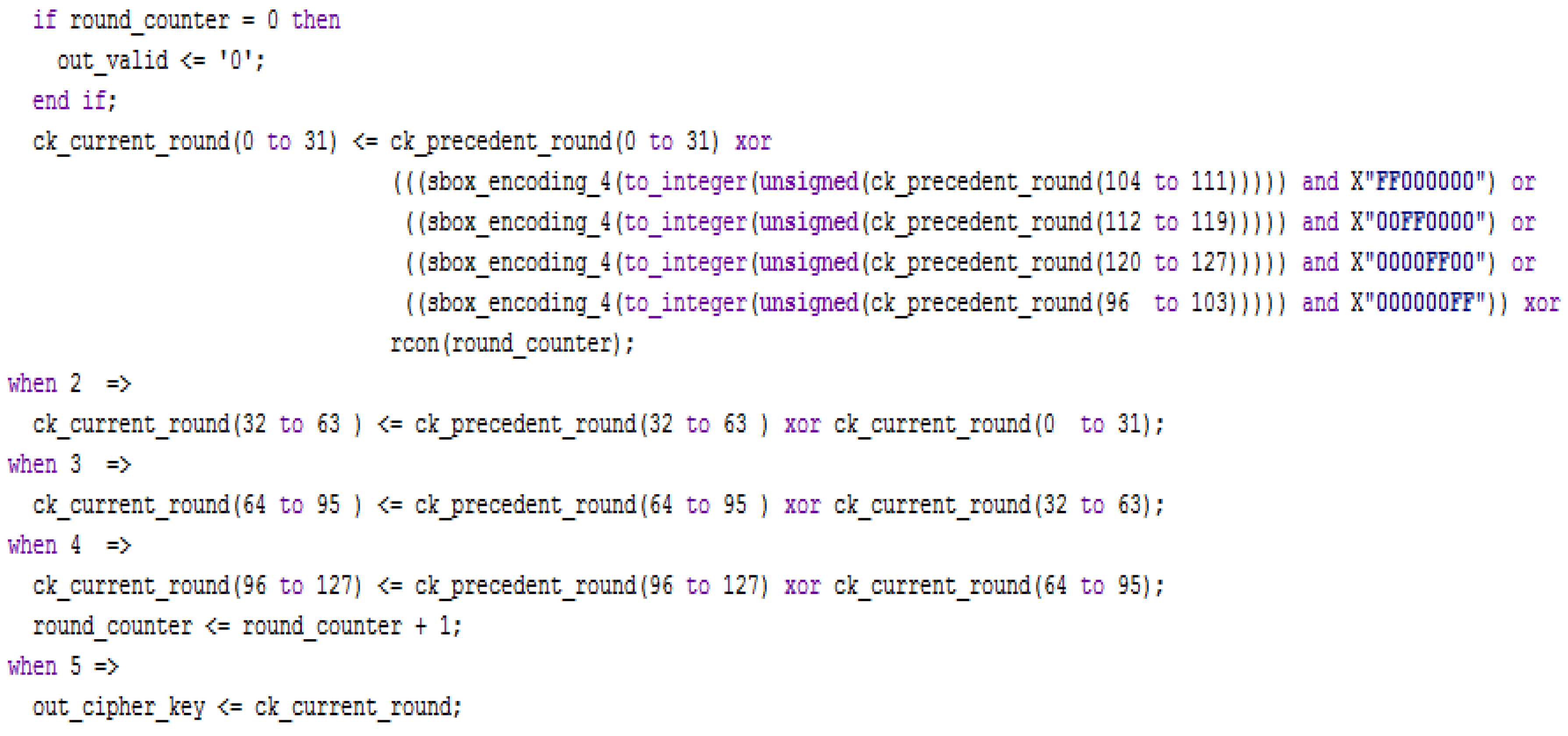
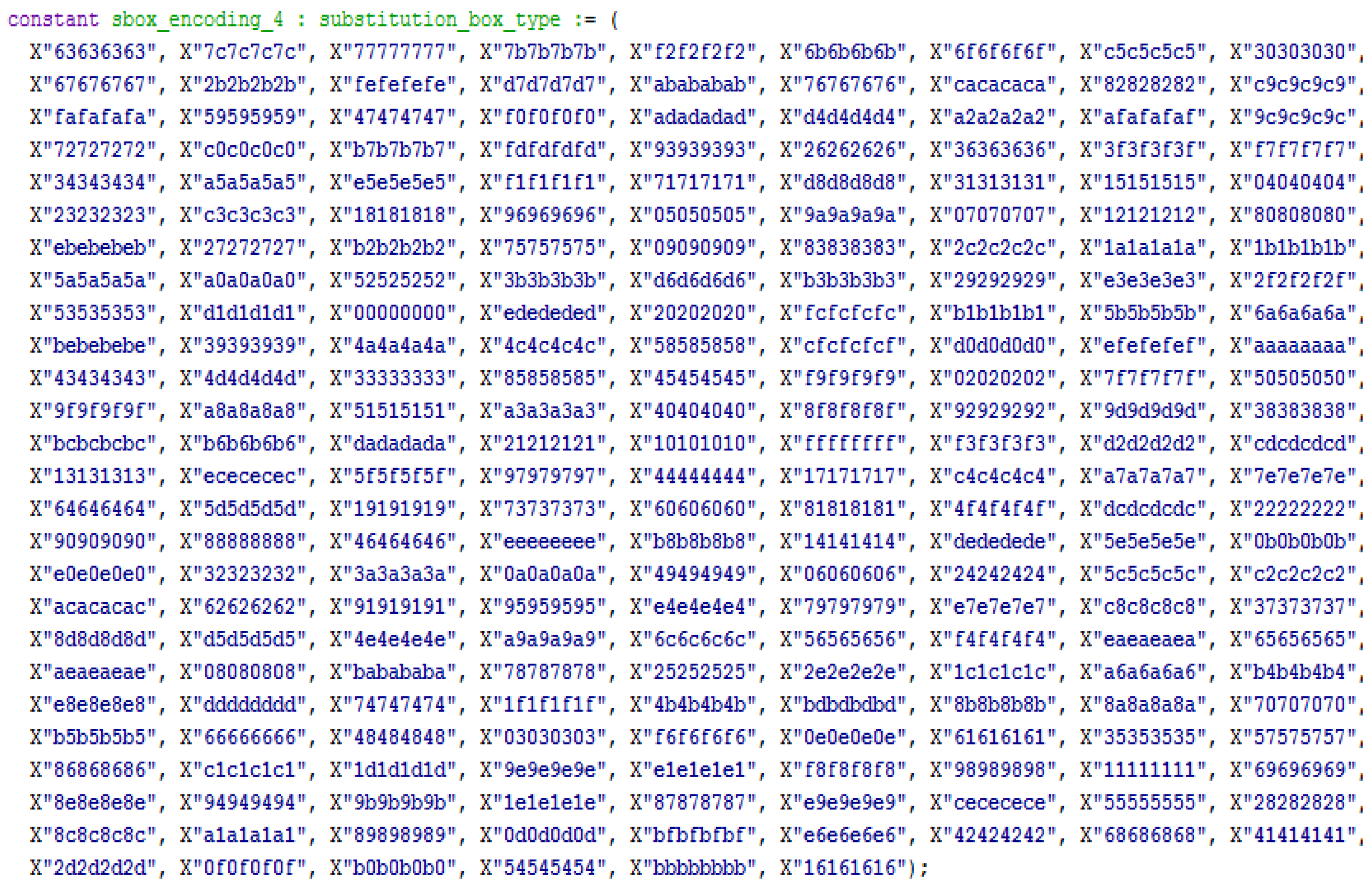
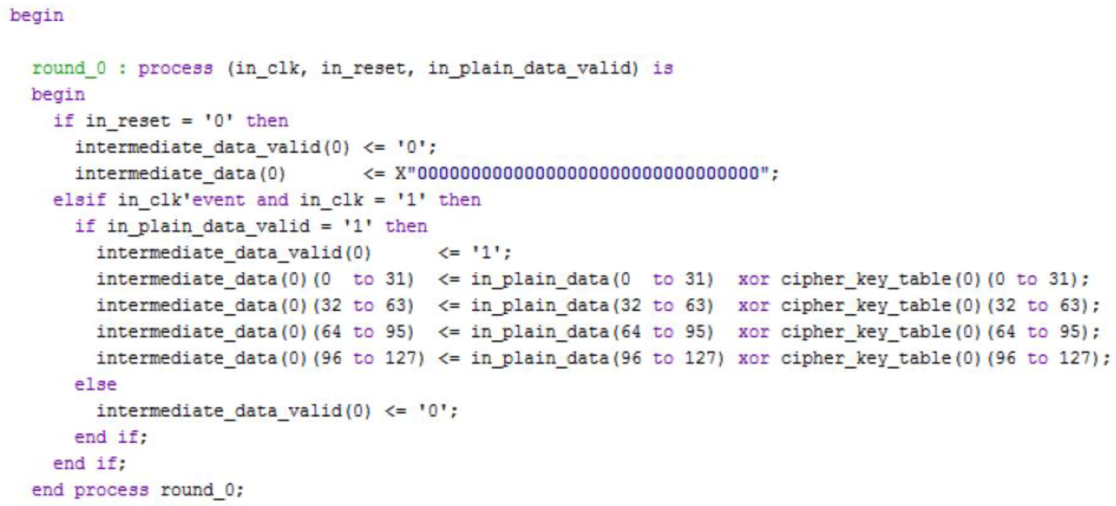
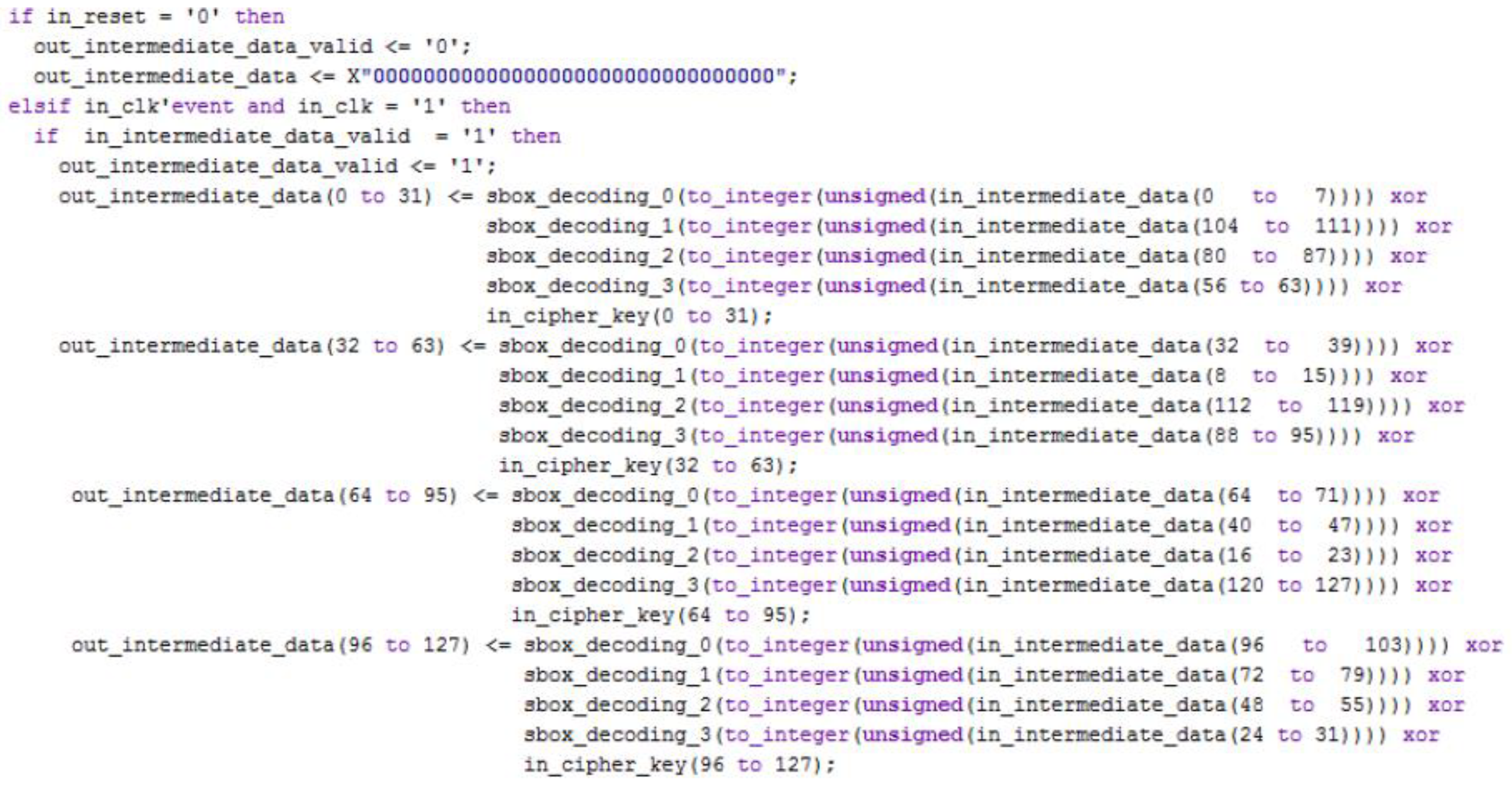
2.1. Fundamentals of the AES-128 Encryption/Decryption Algorithm
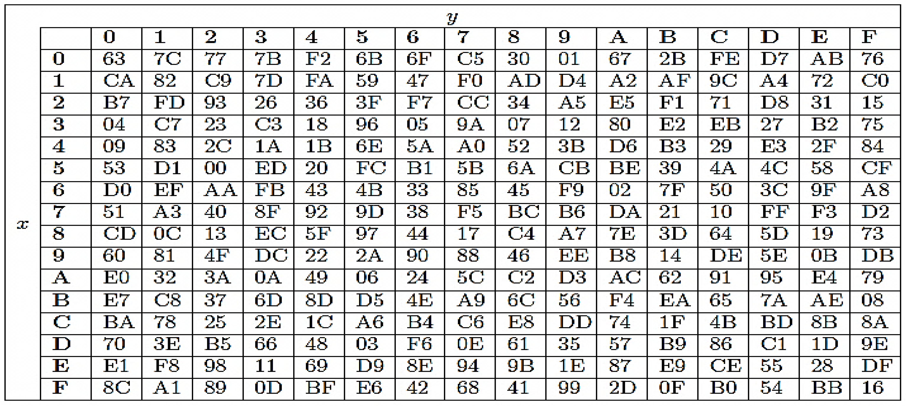
- Substitute Bytes
- Shift Rows
- Mix Columns
- Add Round Key
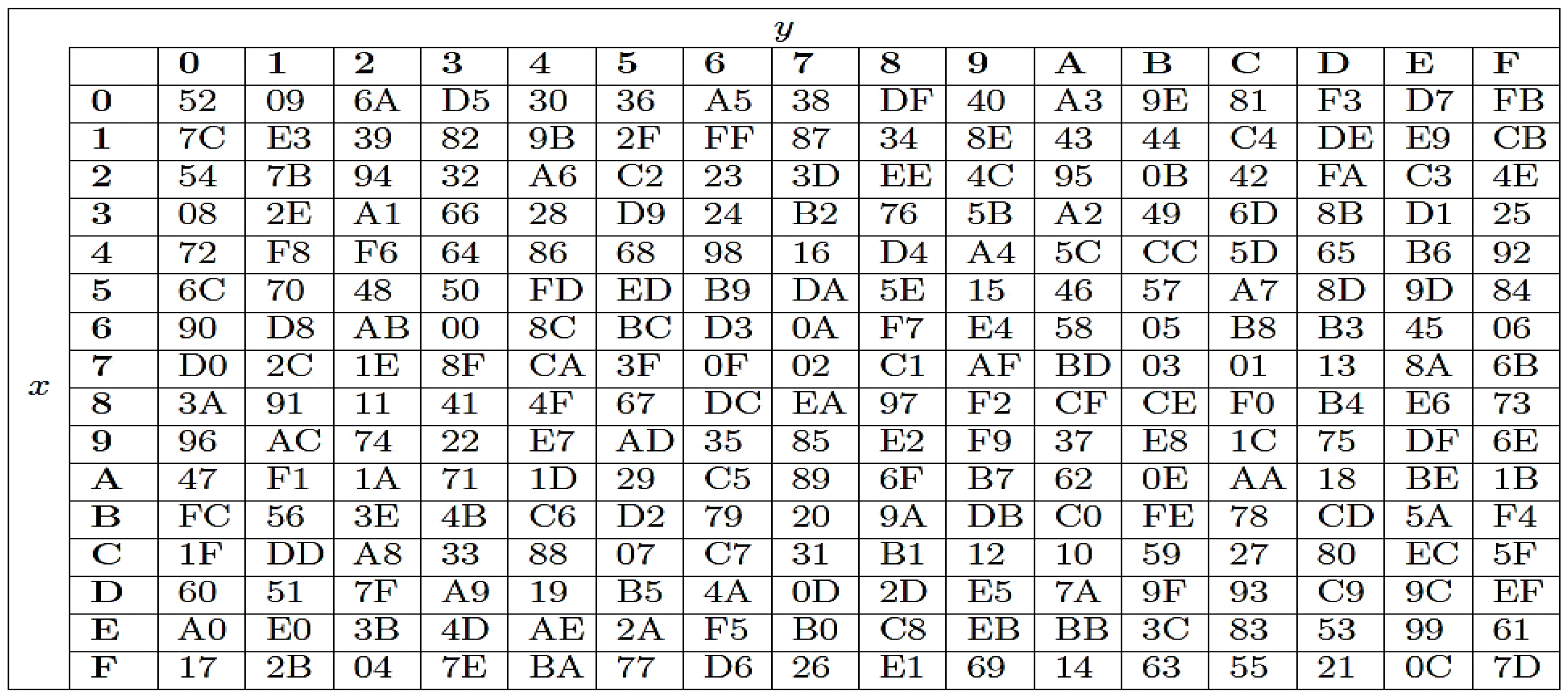
- Inverse Sub Bytes
- Inverse Shift Rows
- Inverse Mix Columns
- Add Round Key
2.2. Implementation of Encrypting/Decrypting Algorithms With FPGA Platforms
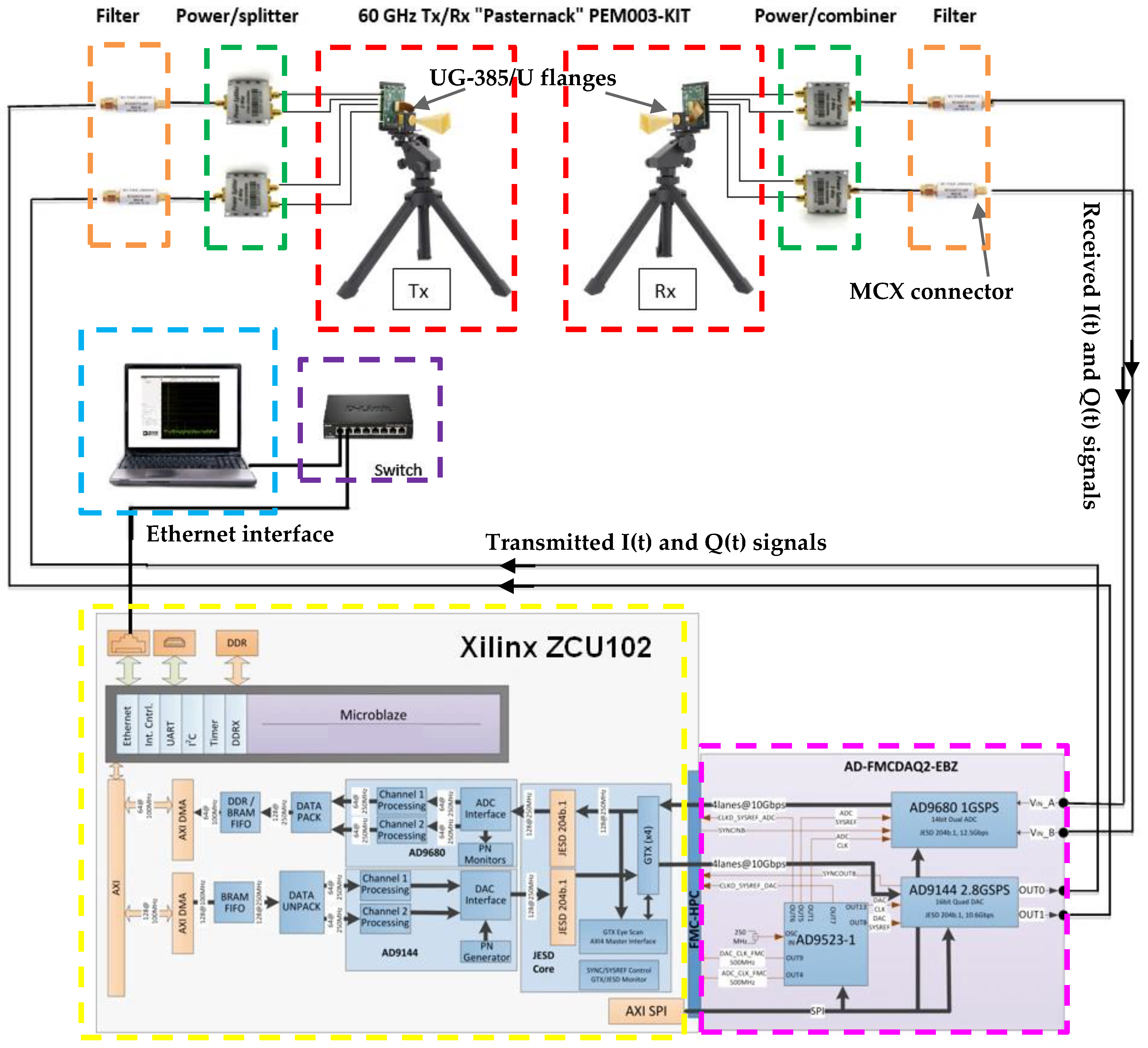
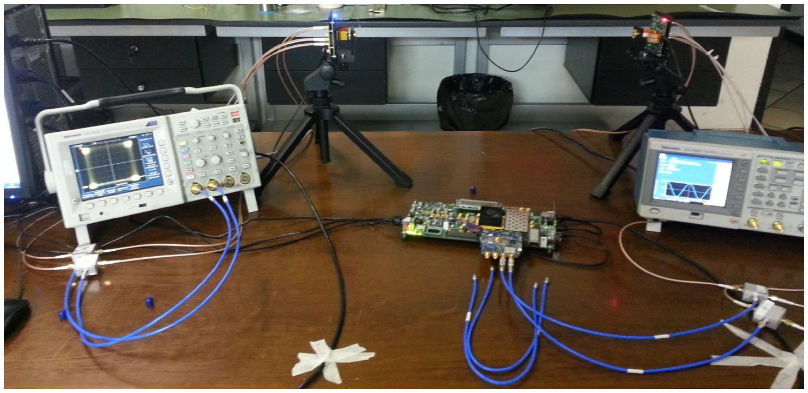
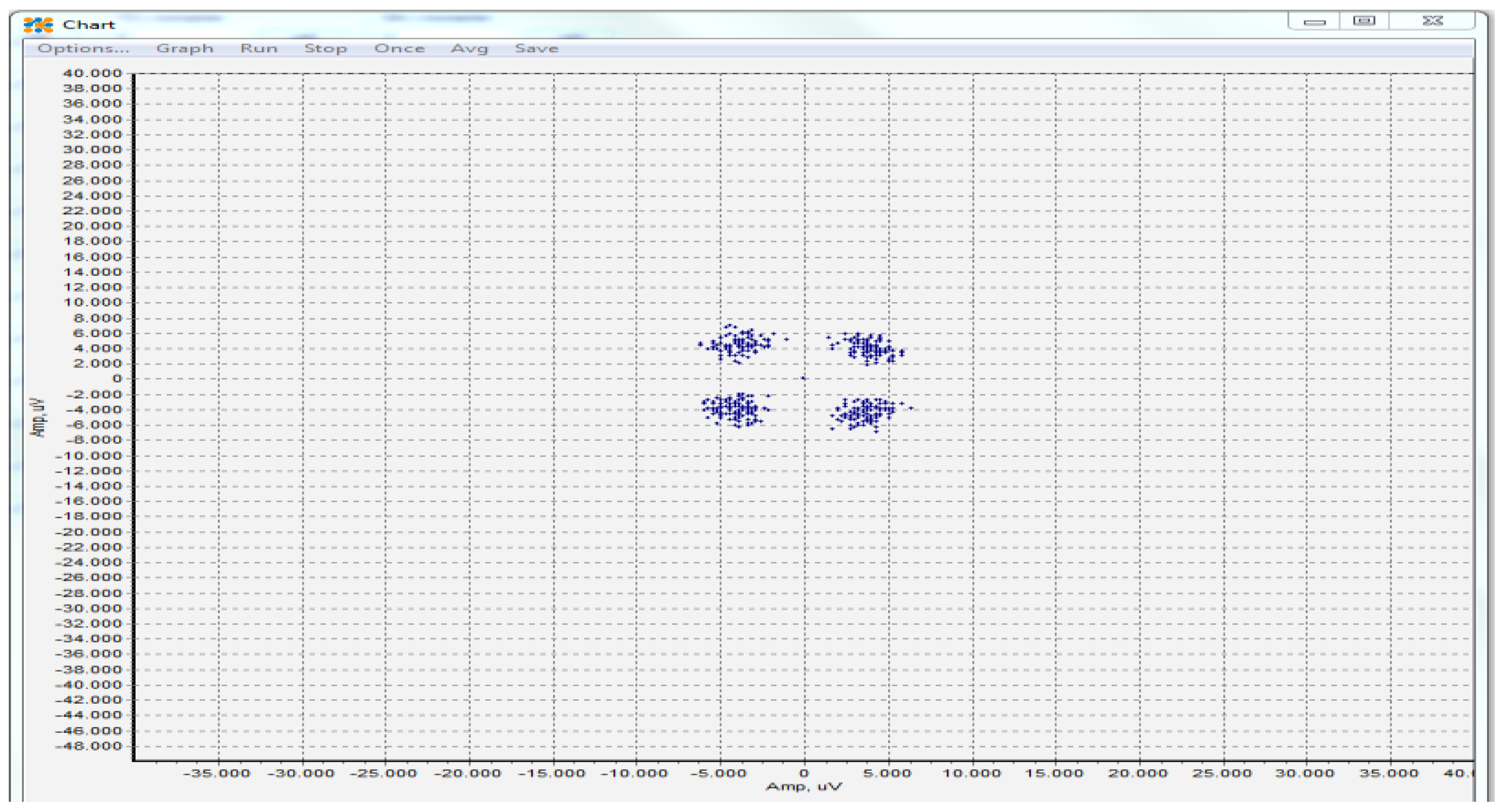
2.3. Description of the “Wireless Connector” System’s Demonstrator and Relative Communication Tests
3. Results
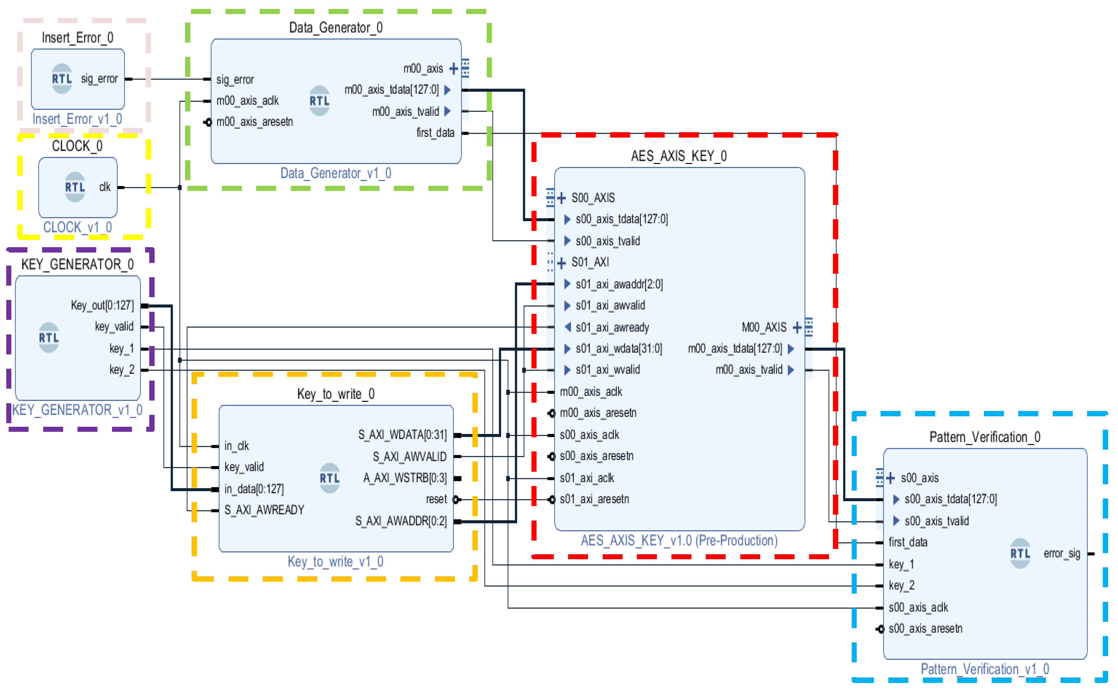
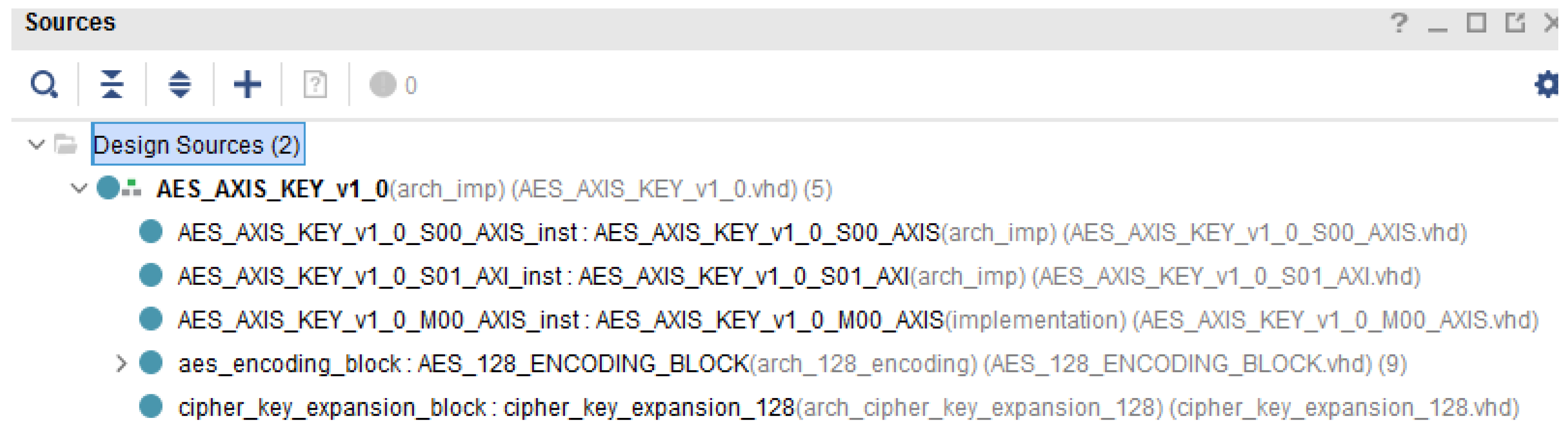
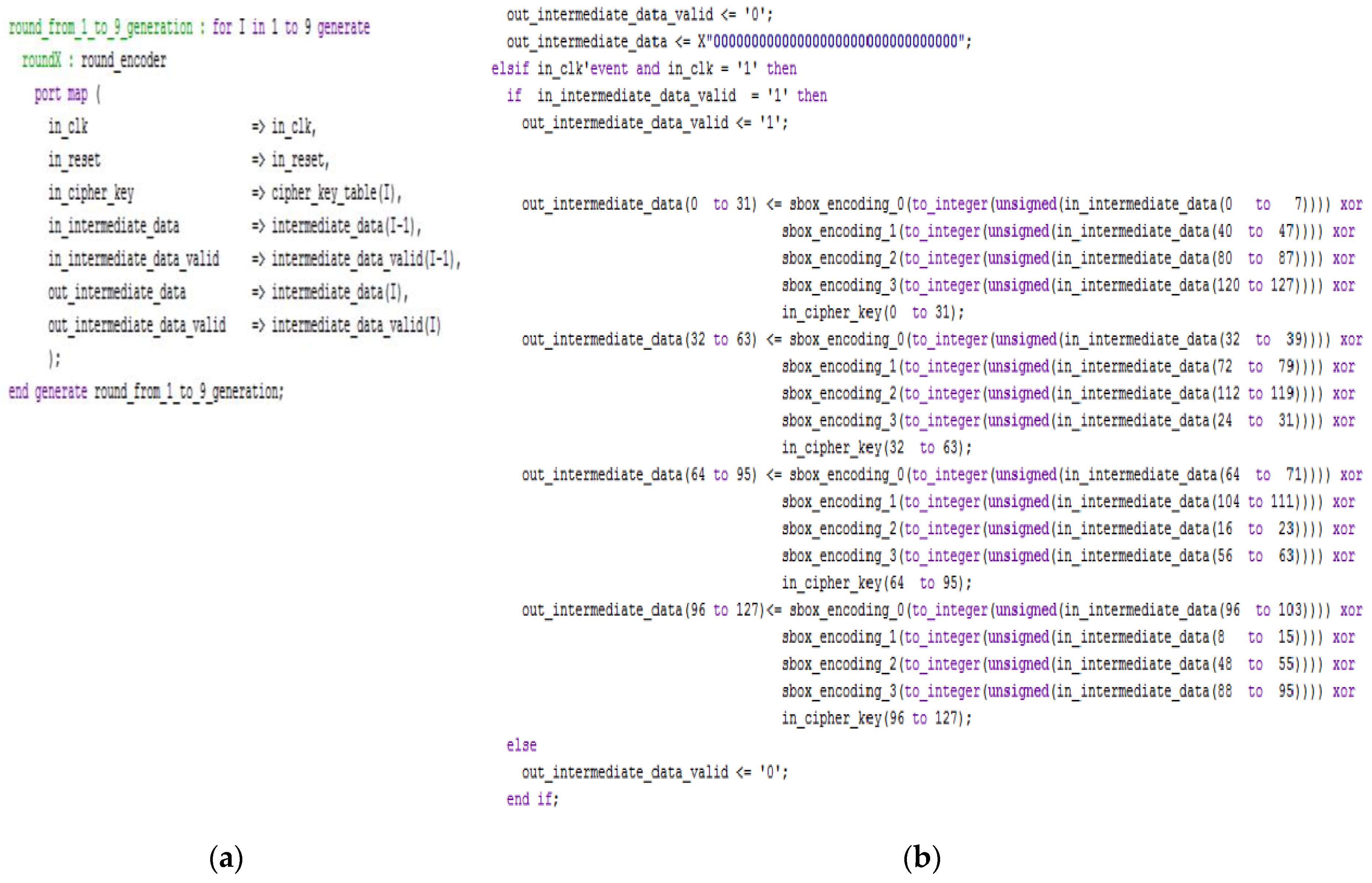
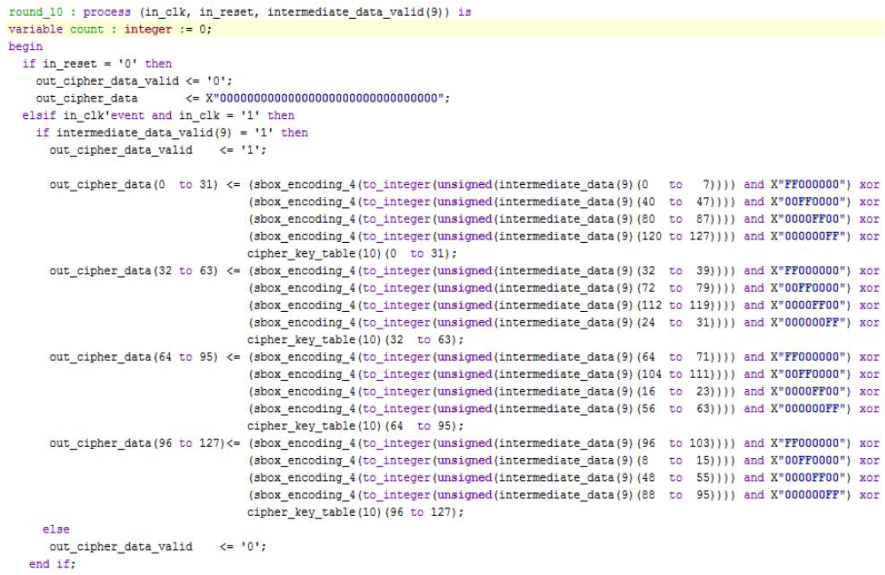
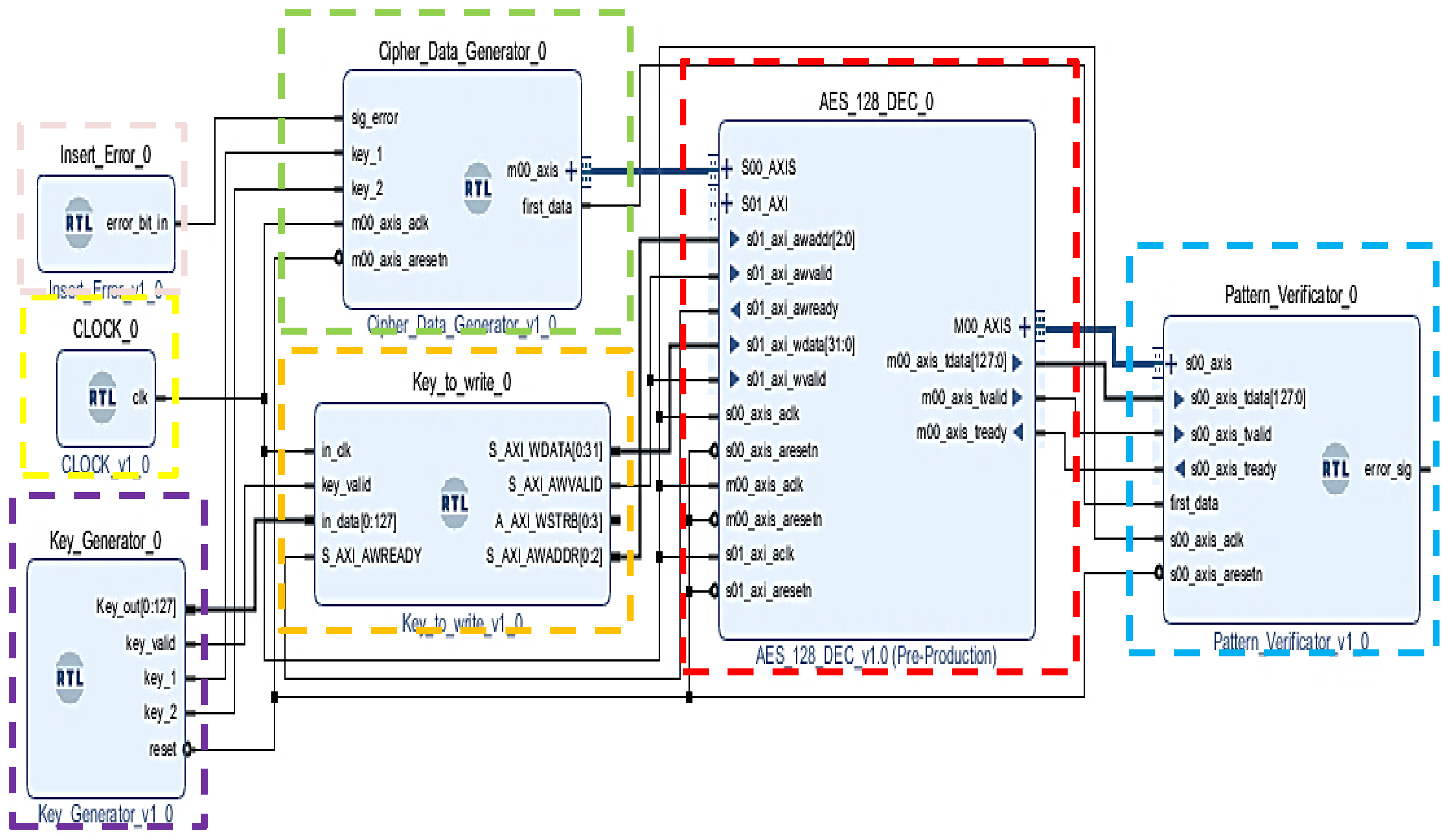
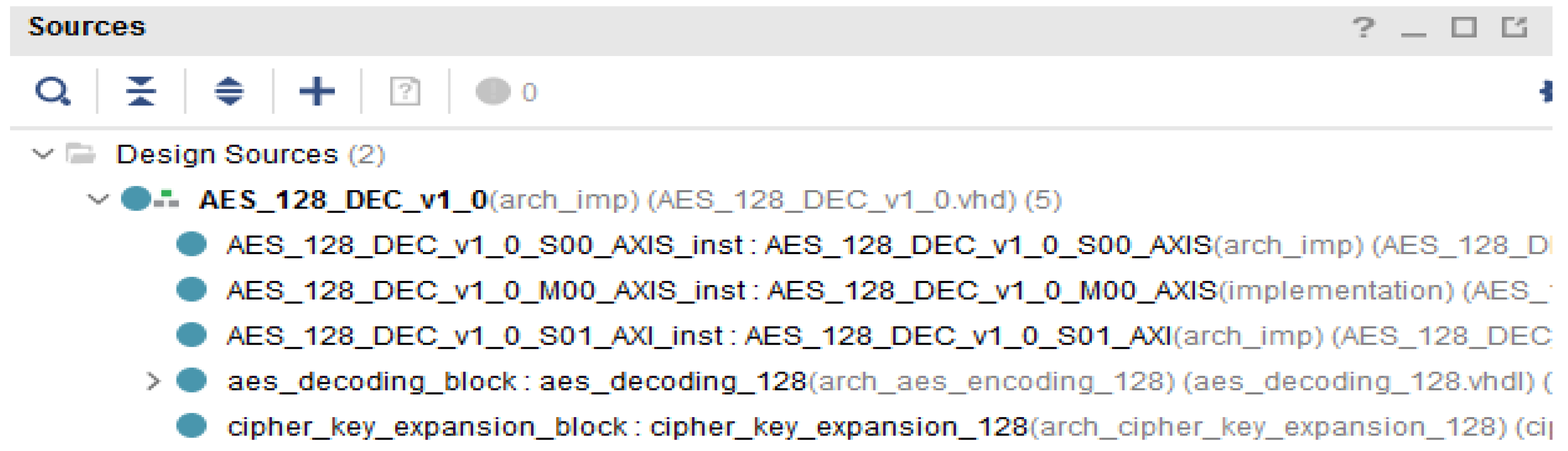
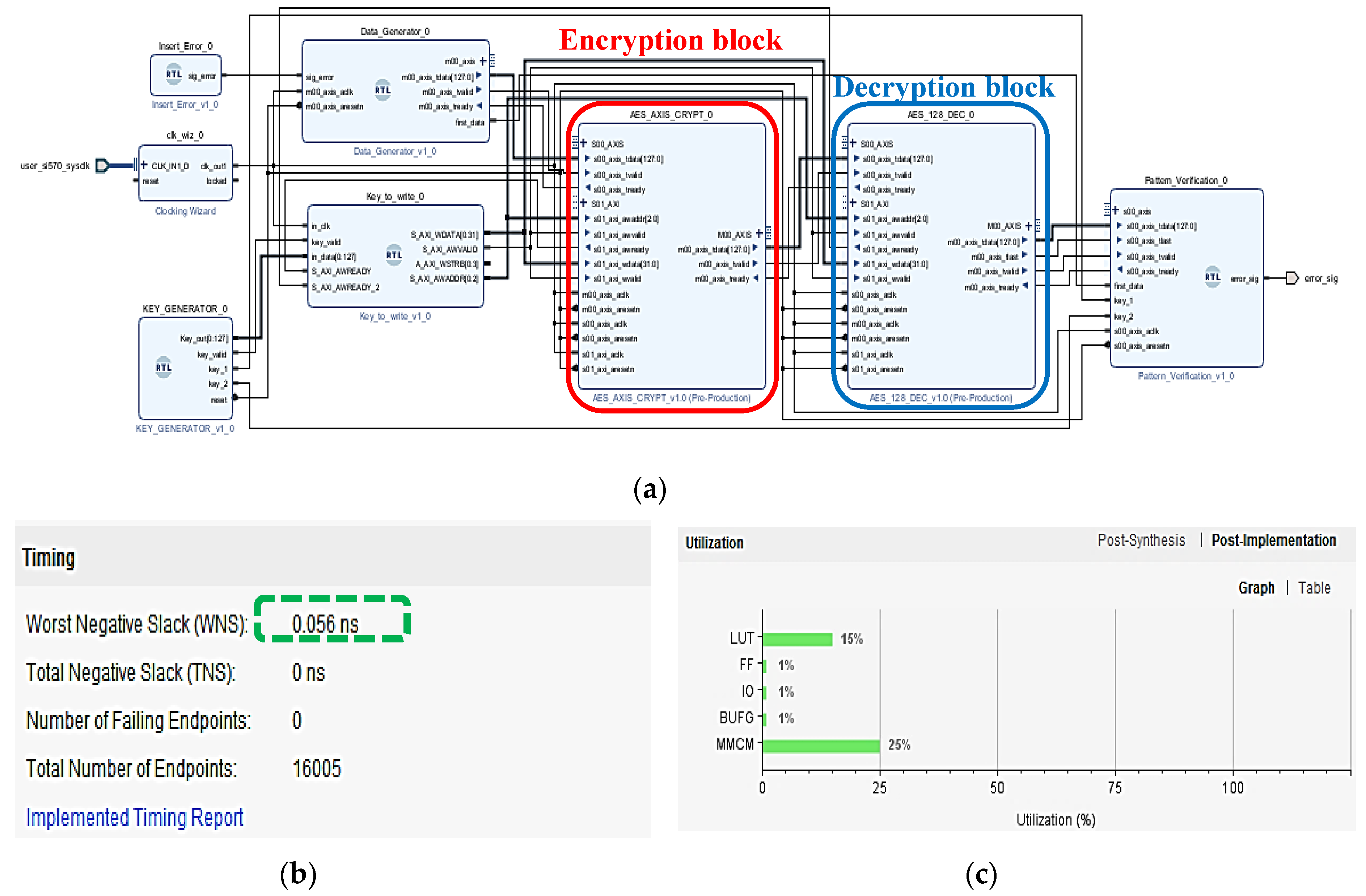
3.1. Description of the VHDL Blocks Implemented for the AES Encryption/Decryption Algorithm
3.2. Post-Synthesis Simulation Results: Resources Utilization of the Encryption/Decryption Systems
4. Discussion
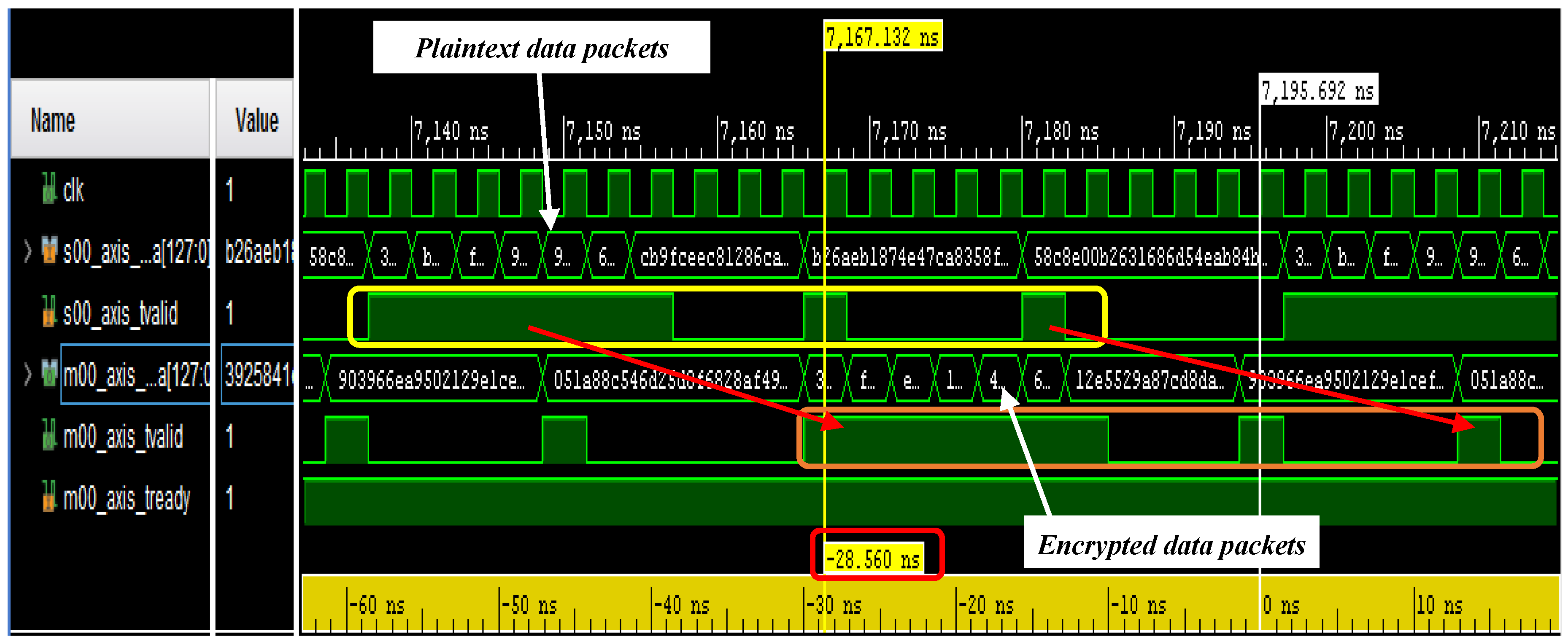
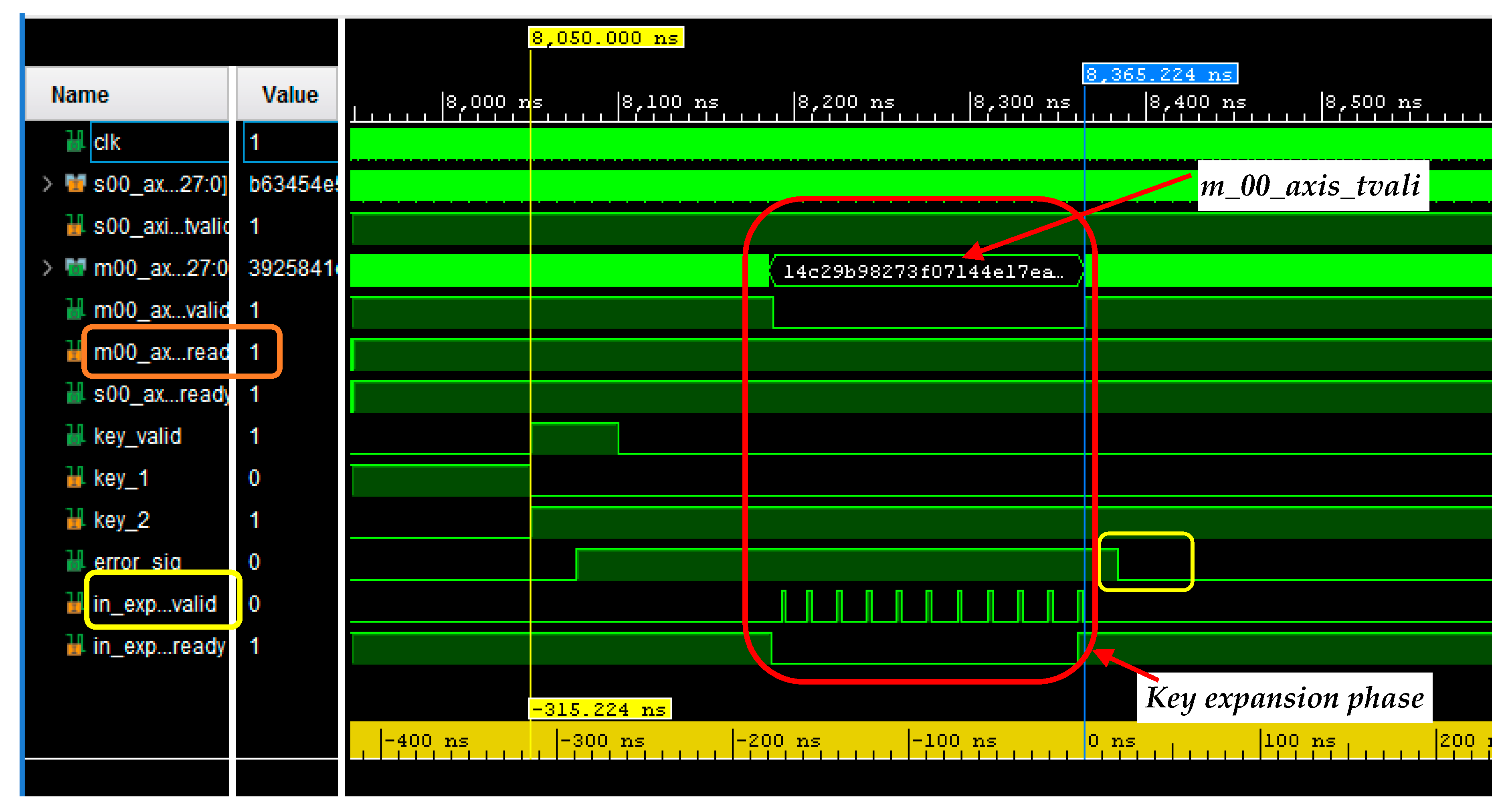
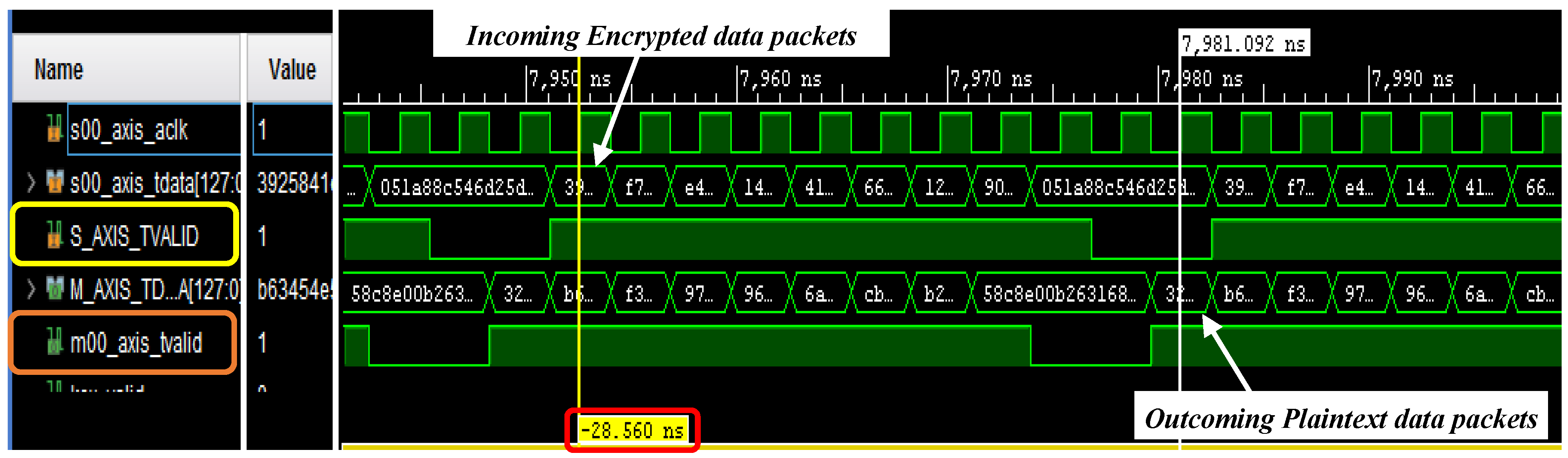
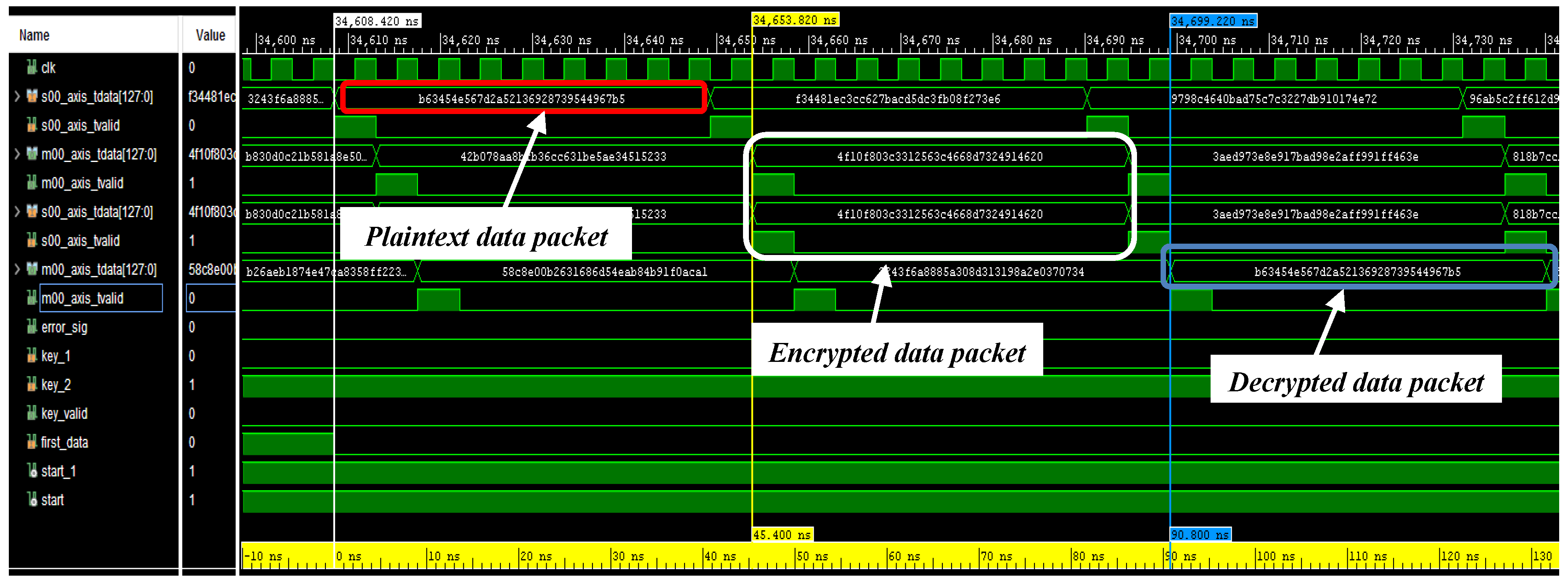
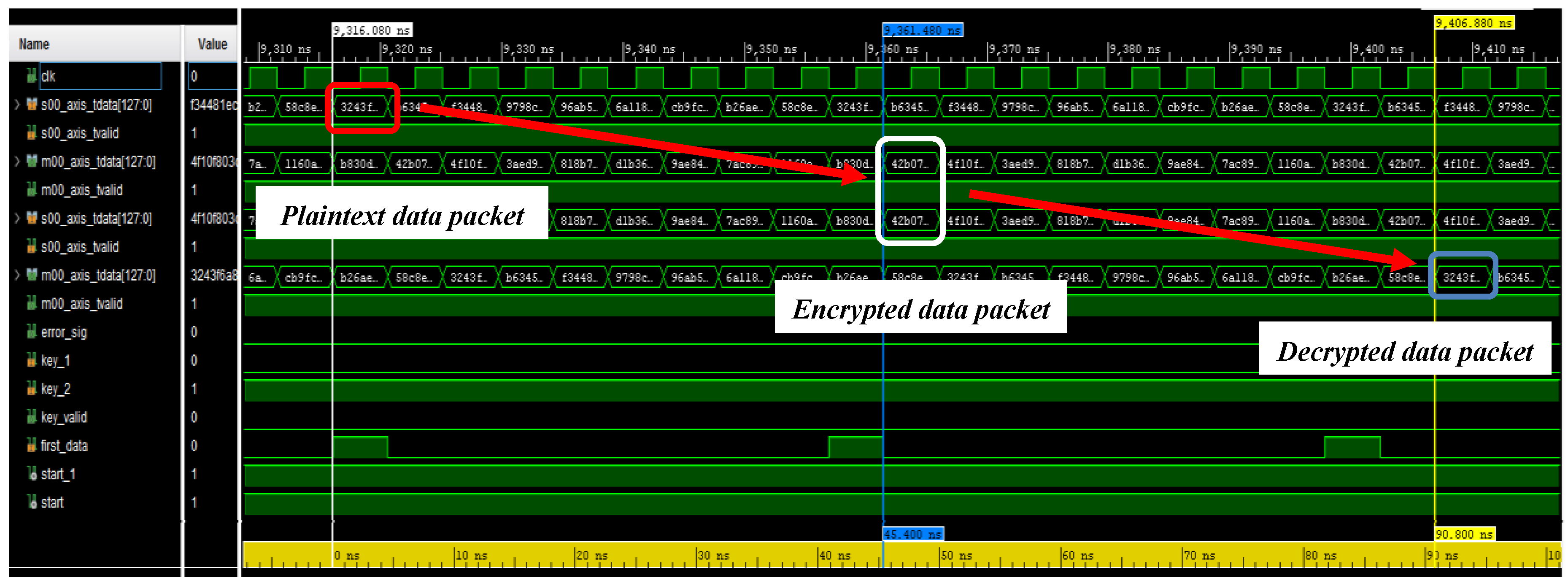
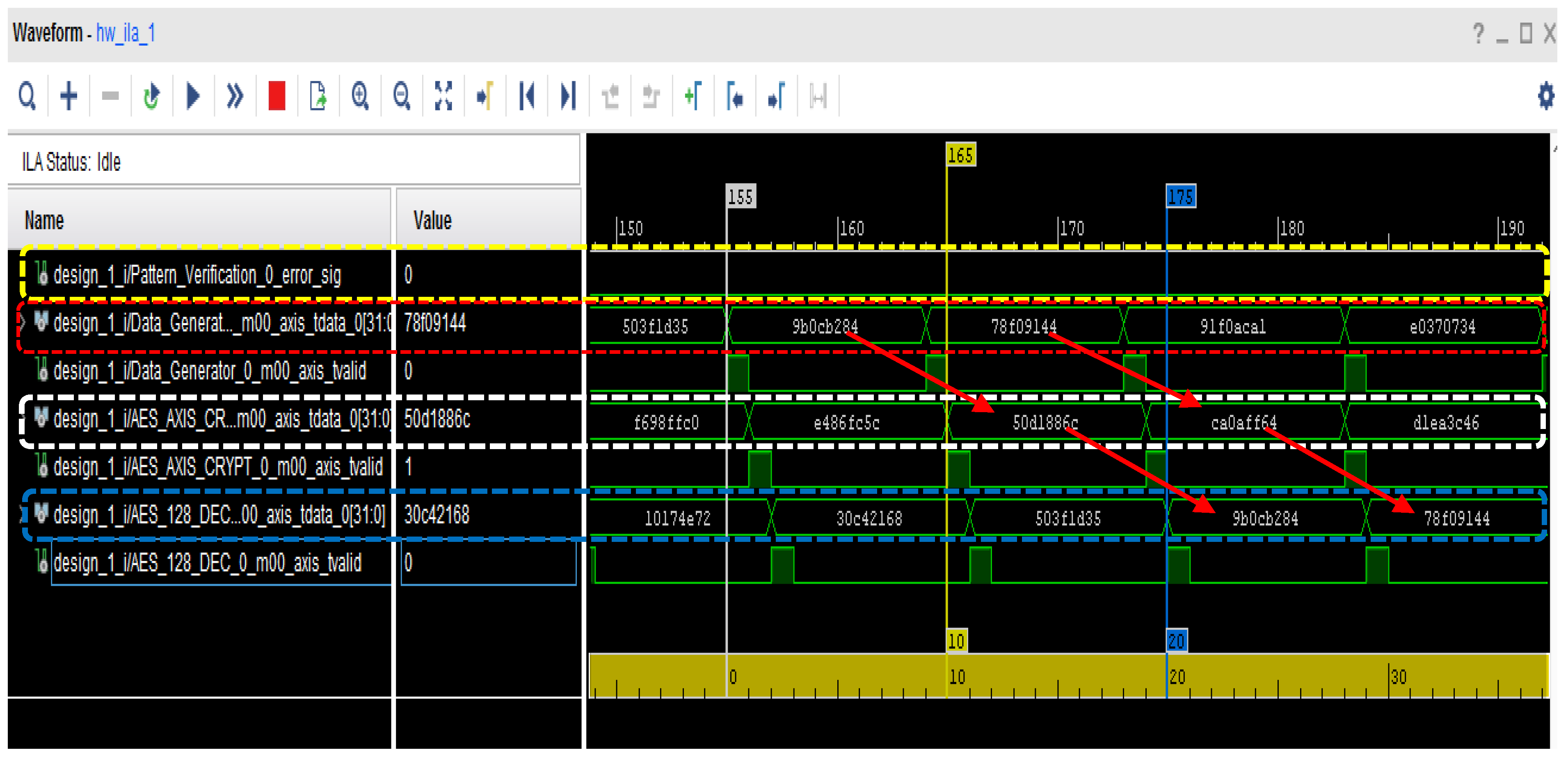
4.1. Post-Implementation Simulations: Clock Routing Issues and Overall Performances of the Combined Encryption/Decryption System
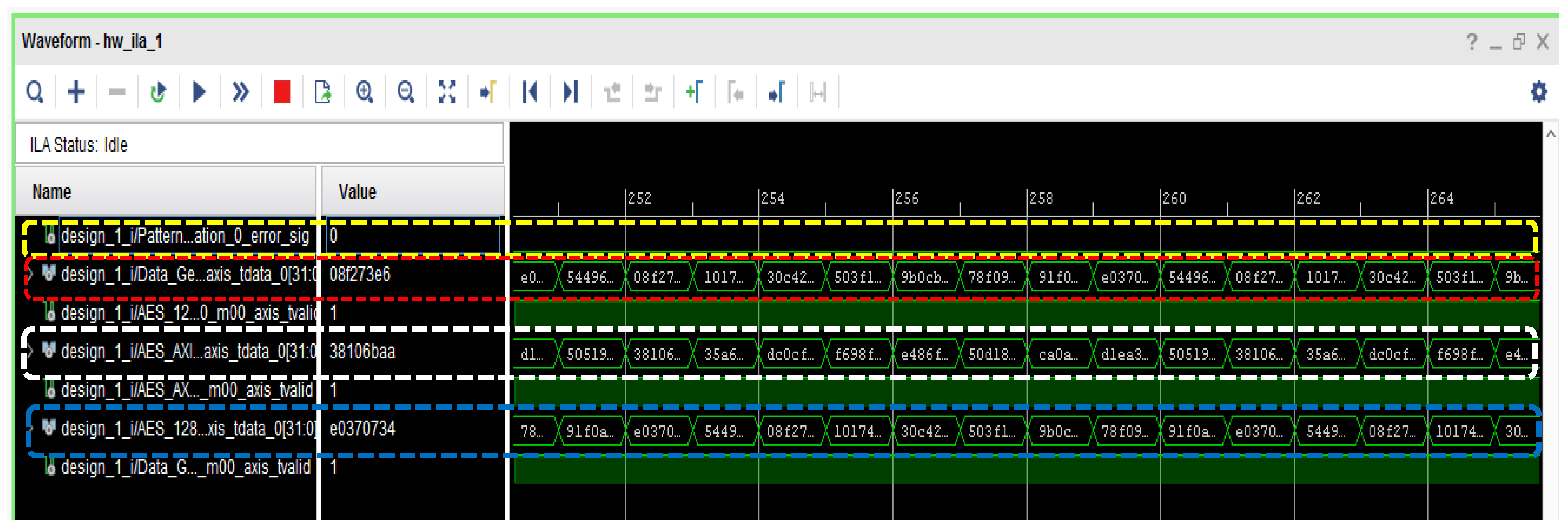
4.2. Testing of the Developed Encryption/Decryption Algorithm on ZCU102 Evaluation Board
4.3. Comparison of the Proposed AES-128 Implementation with Other Works Reported in the Literature
5. Conclusions
Author Contributions
Funding
Conflicts of Interest
References
- Li, L.; Li, S. High throughput AES encryption/decryption with efficient reordering and merging techniques. In Proceedings of the 2017 27th International Conference on Field Programmable Logic and Applications (FPL), Gent, Belgium, 4–6 September 2017; IEEE: Piscataway, NJ, USA, 2017; pp. 1–4. [Google Scholar]
- Wei, J.; Han, J.; Cao, S. Satellite IoT Edge Intelligent Computing: A Research on Architecture. Electronics 2019, 8, 1247. [Google Scholar] [CrossRef]
- De Fazio, R.; Cafagna, D.; Marcuccio, G.; Minerba, A.; Visconti, P. A Multi-Source Harvesting System Applied to Sensor-Based Smart Garments for Monitoring Workers’ Bio-Physical Parameters in Harsh Environments. Energies 2020, 13, 2161. [Google Scholar] [CrossRef]
- Visconti, P.; de Fazio, R.; Costantini, P.; Miccoli, S.; Cafagna, D. Innovative complete solution for health safety of children unintentionally forgotten in a car: A smart Arduino-based system with user app for remote control. IET Sci. Meas. Technol. 2020, 14, 665–675. [Google Scholar] [CrossRef]
- Rajasekar, P.; Haridas, M. Efficient FPGA implementation of AES 128 bit for IEEE 802.16e mobile WiMax standards. Circuits Syst. 2016, 7, 371–380. [Google Scholar] [CrossRef]
- Denning, D.; Irvine, J.; Harold, N.; Dunn, P.; Devlin, M. An implementation of a gigabit Ethernet AES encryption engine for application processing in SDR. In Proceedings of the 2004 IEEE 60th Vehicular Technology Conference, VTC2004-Fall. 2004, Los Angeles, CA, USA, 26–29 September 2004; IEEE: Piscataway, NJ, USA, 2004; Volume 3, pp. 1963–1967. [Google Scholar]
- Dey, A.; Nandi, S.; Sarkar, M. Security Measures in IOT based 5G Networks. In Proceedings of the 2018 3rd International Conference on Inventive Computation Technologies (ICICT), Coimbatore, India, 15–16 November 2018; IEEE: Piscataway, NJ, USA, 2018; pp. 561–566. [Google Scholar]
- Del-Valle-Soto, C.; Velázquez, R.; Valdivia, L.J.; Giannoccaro, N.I.; Visconti, P. An Energy Model Using Sleeping Algorithms for Wireless Sensor Networks under Proactive and Reactive Protocols: A Performance Evaluation. Energies 2020, 13, 3024. [Google Scholar] [CrossRef]
- Visconti, P.; Sbarro, B.; Primiceri, P.; de Fazio, R.; Ekuakille, A.L. Design and Testing of a Telemetry System Based on STM X-Nucleo Board for Detection and Wireless Transmission of Sensors Data Applied to a Single-Seat Formula SAE Car. Int. J. Electron. Telecommun. 2019, 65, 671–678. [Google Scholar] [CrossRef]
- Visconti, P.; Sbarro, B.; Primiceri, P. A ST X-Nucleo-based telemetry unit for detection and WiFi transmission of competition car sensors data: Firmware development, sensors testing and real-time data analysis. Int. J. Smart Sens. Intell. Syst. 2017, 10, 793–828. [Google Scholar] [CrossRef]
- Long, K.; Leung, V.C.M.; Haijun, Z.; Feng, Z.; Li, Y.; Zhang, Z. 5G for Future Wireless Networks, 1st ed.; Springer: Beijing, China, 2017; pp. 1–653. ISBN 978-3-319-72822-3. [Google Scholar]
- Hejazi, A.; Pu, Y.; Lee, K.-Y. A Design of Wide-Range and Low Phase Noise Linear Transconductance VCO with 193.76 dBc/Hz FoMT for mm-Wave 5G Transceivers. Electronics 2020, 9, 935. [Google Scholar] [CrossRef]
- Ghanim, A.; Alshaikhli, I.; Fakhri, T. Comparative study on 4G/LTE cryptographic algorithms based on different factors. Int. J. Comput. Sci. Telecommun. 2014, 5, 7–10. [Google Scholar]
- Park, J.; Park, Y. Symmetric-Key Cryptographic Routine Detection in Anti-Reverse Engineered Binaries Using Hardware Tracing. Electronics 2020, 9, 957. [Google Scholar] [CrossRef]
- Bellemou, A.M.; García, A.; Castillo, E.; Benblidia, N.; Anane, M.; Álvarez-Bermejo, J.A.; Parrilla, L. Efficient Implementation on Low-Cost SoC-FPGAs of TLSv1.2 Protocol with ECC_AES Support for Secure IoT Coordinators. Electronics 2019, 8, 1238. [Google Scholar] [CrossRef]
- Baldoni, W.M.; Ciliberto, C.; Cattaneo, G.M.P. Aritmetica, Crittografia e Codici; Springer: Berlin/Heidelberg, Germany, 2007; ISBN 978-88-470-0456-6. [Google Scholar]
- Saggese, G.P.; Mazzeo, A.; Mazzocca, N.; Strollo, A.G.M. An FPGA-Based Performance Analysis of the Unrolling, Tiling and Pipelining of the AES Algorithm. In Field Programmable Logic and Application; Cheung, P.Y.K., Constantinides, G.A., Eds.; Springer: Berlin/Heidelberg, Germany, 2003; pp. 292–302. [Google Scholar]
- Farooq, U.; Aslam, M.F. Comparative analysis of different AES implementation techniques for efficient resource usage and better performance of an FPGA. J. King Saud Univ. Comput. Inf. Sci. 2017, 29, 295–302. [Google Scholar] [CrossRef]
- Xilinx ZCU102 Evaluation Board User Guide. Available online: https://www.xilinx.com/support/documentation/boards_and_kits/zcu102/ug1182-zcu102-eval-bd.pdf (accessed on 16 September 2020).
- Paar, C.; Pelzl, J. The Advanced Encryption Standard (AES). In Understanding Cryptography: A Textbook for Students and Practitioners; Paar, C., Pelzl, J., Eds.; Springer: Berlin/Heidelberg, Germany, 2010; pp. 87–121. ISBN 978-3-642-04101-3. [Google Scholar]
- Rahimunnisa, K.; Karthigaikumar, P.; Rasheed, S.; Jayakumar, J.; SureshKumar, S. FPGA implementation of AES algorithm for high throughput using folded parallel architecture. Secur. Commun. Networks 2014, 7, 2225–2236. [Google Scholar] [CrossRef]
- Guzmán, I.; Nieto, R.; Noreña, Á. FPGA implementation of the AES-128 algorithm in non-feedback modes of operation. DYNA 2016, 83, 37–43. [Google Scholar] [CrossRef]
- Noorbasha, F.; Divya, Y.; Poojitha, M.; Navya, K.; Bhavishya, A.; Rao, K.; Kishore, K. FPGA design and implementation of modified AES based encryption and decryption algorithm. Int. J. Innov. Technol. Explor. Eng. 2019, 8, 132–136. [Google Scholar]
- Gopalan, A.; Ganesh, J.; Swathi, M. FPGA-based Message Encryption and Decryption. Int. J. Innov. Technol. Explor. Eng. 2015, 4, 1225–1232. [Google Scholar]
- Fan, C.-P.; Hwang, J.-K. Implementations of high throughput sequential and fully pipelined AES processors on FPGA. In Proceedings of the 2007 International Symposium on Intelligent Signal Processing and Communication Systems, Xiamen, China, 28 November–1 December 2007; pp. 353–356. [Google Scholar]
- McLoone, M.; McCanny, J.V. High-performance FPGA implementation of DES using a novel method for implementing the key schedule. IEE Proc. Circuits Devices Syst. 2003, 150, 373–378. [Google Scholar] [CrossRef]
- Chodowiec, P.; Gaj, K. Very compact FPGA implementation of the AES algorithm. In Proceedings of the CHES 2003, Cologne, Germany, 8–10 September 2003; Volume 2779, pp. 319–333. [Google Scholar]
- Bani-Hani, R.; Harb, S.; Mhaidat, K.; Taqieddin, E. High-Throughput and Area-Efficient FPGA Implementations of Data Encryption Standard (DES). Circuits Syst. 2014, 5, 45–56. [Google Scholar] [CrossRef]
- Rouvroy, G.; Standaert, F.-X.; Quisquater, J.-J.; Legat, J.-D. Efficient uses of FPGAs for implementations of DES and its experimental linear cryptanalysis. IEEE Trans. Comput. 2003, 52, 473–482. [Google Scholar] [CrossRef]
- Ahmad, N.; Hasan, R.; Jubadi, W.M. Design of AES S-box using combinational logic optimization. In Proceedings of the 2010 IEEE Symposium on Industrial Electronics and Applications (ISIEA), Penang, Malaysia, 3–6 October 2010; IEEE: Piscataway, NJ, USA, 2010; pp. 696–699. [Google Scholar]
- Canright, D. A Very Compact S-Box for AES. In Cryptographic Hardware and Embedded Systems–CHES 2005; Rao, J.R., Sunar, B., Eds.; Springer: Berlin/Heidelberg, Germany, 2005; pp. 441–455. [Google Scholar]
- Satoh, A.; Morioka, S.; Takano, K.; Munetoh, S. A Compact Rijndael Hardware Architecture with S-Box Optimization. In International Conference on the Theory and Application of Cryptology and Information Security: Advances in Cryptology; Springer: Berlin/Heidelberg, Germany, 2001; pp. 239–254. [Google Scholar]
- Good, T.; Benaissa, M. AES on FPGA from the Fastest to the Smallest. In Cryptographic Hardware and Embedded Systems–CHES 2005; Rao, J.R., Sunar, B., Eds.; Springer: Berlin/Heidelberg, Germany, 2005; pp. 427–440. [Google Scholar]
- Murugeswari, S.; Sridevi, P.; Vanaja, D.; Vanaja, G. Area optimization for reducing circuit complexity in masked AES based on FPGA. Int. J. Innov. Emerg. Technol. 2015, 1, 1–4. [Google Scholar]
- Sutharsan, H.; Thomas, A. Area & Power optimization of AES algorithm using modified mixcolumn with composite S-BOX. IJRSET 2016, 3, 12–24. [Google Scholar]
- Hua, L.; Friggstad, Z. An efficient architecture for the AES mix columns operation. In Proceedings of the 2005 IEEE International Symposium on Circuits and Systems, Kobe, Japan, 23–26 May 2005; IEEE: Piscataway, NJ, USA, 2005; Volume 5, pp. 4637–4640. [Google Scholar]
- Xilinx UltraScale Architecture Configurable Logic Block User Guide (UG574). Available online: https://www.xilinx.com/support/documentation/user_guides/ug574-ultrascale-clb.pdf (accessed on 26 August 2020).
- Zambreno, J.; Nguyen, D.; Choudhary, A. Exploring Area/Delay Tradeoffs in an AES FPGA Implementation. In Field Programmable Logic and Application; Becker, J., Platzner, M., Vernalde, S., Eds.; Springer: Berlin/Heidelberg, Germany, 2004; pp. 575–585. [Google Scholar]
- Bulens, P.; Standaert, F.-X.; Quisquater, J.-J.; Pellegrin, P.; Rouvroy, G. Implementation of the AES-128 on Virtex-5 FPGAs. In Progress in Cryptology–AFRICACRYPT 2008; Vaudenay, S., Ed.; Springer: Berlin/Heidelberg, Germany, 2008; pp. 16–26. [Google Scholar]
- Standaert, F.-X.; Rouvroy, G.; Quisquater, J.-J.; Legat, J.-D. Efficient Implementation of Rijndael Encryption in Reconfigurable Hardware: Improvements and Design Tradeoffs. In Cryptographic Hardware and Embedded Systems—CHES 2003; Walter, C.D., Koç, Ç.K., Paar, C., Eds.; Springer: Berlin/Heidelberg, Germany, 2003; pp. 334–350. [Google Scholar]
- Hodjat, A.; Verbauwhede, I. A 21.54 Gbits/s fully pipelined AES processor on FPGA. In Proceedings of the 12th Annual IEEE Symposium on Field-Programmable Custom Computing Machines, Napa, CA, USA, 20–23 April 2004; IEEE: Piscataway, NJ, USA, 2004; pp. 308–309. [Google Scholar]
- Kotturi, D.; Seong-Moo, Y.; Blizzard, J. AES crypto chip utilizing high-speed parallel pipelined architecture. In Proceedings of the 2005 IEEE International Symposium on Circuits and Systems, Kobe, Japan, 23–26 May 2005; IEEE: Piscataway, NJ, USA, 2005; Volume 5, pp. 4653–4656. [Google Scholar]
- Daoud, L.; Hussein, F.; Rafla, N. Optimization of Advanced Encryption Standard (AES) Using Vivado High Level Synthesis (HLS). In Proceedings of the 34th International Conference on Computers and Their Applications, Honolulu, HI, USA, 18–20 March 2019; Volume 58, pp. 36–44. [Google Scholar]


| Simulation | Resource | Utilization | Utilization [%] |
|---|---|---|---|
| Complete encryption system | LUT | 15,029 | 5.48 |
| FF | 4296 | 0.78 | |
| Encryption block | LUT | 13,043 | 4.76 |
| FF | 3877 | 0.71 |
| Simulation | Resource | Utilization | Utilization [%] |
|---|---|---|---|
| Complete decryption system (350 MHz packet rate) | LUT | 29,111 | 10.62 |
| FF | 4339 | 0.79 | |
| BUFG | 1 | 0.25 | |
| Complete decryption system (23.4 MHz packet rate) | LUT | 29,156 | 10.64 |
| FF | 4339 | 0.79 | |
| BUFG | 1 | 0.25 | |
| Decryption block | LUT | 27,713 | 10.11 |
| FF | 3912 | 0.71 | |
| BUFG | 1 | 0.25 |
| Clock Frequency [MHz] | Worst Negative Slack [ns] | Total Negative Slack [ns] |
|---|---|---|
| 180 | 0.056 | 0 |
| 190 | 0 | 0 |
| 200 | −0.199 | −0.353 |
| 250 | −0.441 | −0.895 |
| Design. | Platform | Frequency [MHz] | Throughput [Gbit/s] | Slices | Efficiency [Mbps/slice] |
|---|---|---|---|---|---|
| Zambreno J. et al. [38] (Enc) | XC2V4000 | 184.1 | 23.57 | 16,938 | 1.39 |
| Fan C.P. et al. [25] (Enc) | XC4VLX200 | 250.0 | 32.00 | 86,806 | 0.36 |
| Bulens P. et al. [39] (Enc) | Virtex-4 | 250.0 | 2.90 | 1220 | 2.30 |
| Standaert F. et al. [40] (Enc) | XCV3200E8 | 145.0 | 18.56 | 10,750 | 1.66 |
| Hodjat A. et al. [41] (Enc) | XC2VP20-7 | 168.3 | 21.54 | 5177 | 4.16 |
| Kotturi D. et al. [42] (Enc) | XC2VP70-7 | 232.6 | 29.77 | 5408 | 5.50 |
| Daoud L. et al. [43] (Enc) | XC7Z020 | 192.0 | 1.29 | 431 | 2.99 |
| Good T. et al. [33] (Enc/Dec) | XC3S2000-5 | 196.1 | 23.65 | 16,693 | 1.42 |
| Our solution (Enc) | XCZU9EG | 220.0 | 28.16 | 3262 | 8.63 |
| Our solution (Enc/Dec) | XCZU9EG | 220.0 | 28.16 | 10,278 | 2.74 |
© 2020 by the authors. Licensee MDPI, Basel, Switzerland. This article is an open access article distributed under the terms and conditions of the Creative Commons Attribution (CC BY) license (http://creativecommons.org/licenses/by/4.0/).
Share and Cite
Visconti, P.; Capoccia, S.; Venere, E.; Velázquez, R.; Fazio, R.d. 10 Clock-Periods Pipelined Implementation of AES-128 Encryption-Decryption Algorithm up to 28 Gbit/s Real Throughput by Xilinx Zynq UltraScale+ MPSoC ZCU102 Platform. Electronics 2020, 9, 1665. https://doi.org/10.3390/electronics9101665
Visconti P, Capoccia S, Venere E, Velázquez R, Fazio Rd. 10 Clock-Periods Pipelined Implementation of AES-128 Encryption-Decryption Algorithm up to 28 Gbit/s Real Throughput by Xilinx Zynq UltraScale+ MPSoC ZCU102 Platform. Electronics. 2020; 9(10):1665. https://doi.org/10.3390/electronics9101665
Chicago/Turabian StyleVisconti, Paolo, Stefano Capoccia, Eugenio Venere, Ramiro Velázquez, and Roberto de Fazio. 2020. "10 Clock-Periods Pipelined Implementation of AES-128 Encryption-Decryption Algorithm up to 28 Gbit/s Real Throughput by Xilinx Zynq UltraScale+ MPSoC ZCU102 Platform" Electronics 9, no. 10: 1665. https://doi.org/10.3390/electronics9101665
APA StyleVisconti, P., Capoccia, S., Venere, E., Velázquez, R., & Fazio, R. d. (2020). 10 Clock-Periods Pipelined Implementation of AES-128 Encryption-Decryption Algorithm up to 28 Gbit/s Real Throughput by Xilinx Zynq UltraScale+ MPSoC ZCU102 Platform. Electronics, 9(10), 1665. https://doi.org/10.3390/electronics9101665