Article

Design of a Ka-Band U-Shaped Bandpass Filter with 20-GHz Bandwidth in 0.13-μm BiCMOS Technology

Electronics Design Lab, Singapore University of Technology and Design, 8 Somapah Road, Singapore 487372, Singapore
*
Author to whom correspondence should be addressed.
Electronics 2020, 9(10), 1608; https://doi.org/10.3390/electronics9101608
Submission received: 31 August 2020 / Revised: 24 September 2020 / Accepted: 26 September 2020 / Published: 1 October 2020
(This article belongs to the Special Issue Millimeter-Wave Integrated Circuits and Systems for 5G Applications)

Abstract

:
In this work, the design of a novel Ka-band miniaturized bandpass filter with broad bandwidth is demonstrated by using inversely coupled U-shaped transmission lines. In the proposed filter, two transmission zeros can be generated within a cascaded U-shaped structure and it can also be proven that, by inversely coupling two stacked U-shaped transmission lines, the notch frequency at the upper stopband can be shifted to a lower frequency, which results in a smaller chip size. The key parameters affecting the performance of the proposed filter are investigated in detail with the effective lumped-element circuit illustrated. Fabricated in a 0.13-μm SiGe BiCMOS process, the proposed filter achieves an insertion loss of 3.6 dB at a frequency of 28.75 GHz and the measured bandwidth is from 20.75 GHz to 41 GHz. The return loss is better than −10 dB from 20.5 GHz to 39 GHz. The lower transmission zero is located at 11.75 GHz with a suppression of 54 dB while the upper transmission zero is around 67 GHz with an attenuation of 34.6 dB. The measurement agrees very well with the simulation results and the overall chip size of the proposed filter is 176 × 269 μm2.

1. Introduction

The bandpass filters (BPF) become more and more significant with the emergence of 5G technology, which utilizes millimeter-wave (mm-Wave) as its carrier frequency. Serving as a key block in radio frequency (RF) front-end, the mm-Wave BPF is required to be integrated on-chip for low insertion loss. Besides, it also dominates the images and spurs within the overall communication systems. As the transceiver is commonly implemented in an integrated circuit (IC), the most critical specification for on-chip filters is their footprint due to the expensive process cost. The conventional on-chip filters employ the passive inductors and capacitors, which are usually realized by the lumped components or transmission lines, and hence resulting in large die area even at mm-Wave region. In addition, a large filter size also leads to deteriorated Ohm loss associated with the length of the metal traces. The general idea of a BPF is illustrated in Figure 1 whereby two transmission zeros (TZs) could be introduced as the lower and upper stopband frequencies, respectively. The frequency between the stopband frequencies is the passband.
There is an immense amount of research carried out to achieve TZs in a small area. The conventional method is to use transmission lines based resonators such as stub-loaded resonators [1,2] or stepped-impedance resonators [3,4,5] at the cost of large areas. In [6,7,8,9], the folded micro-strip lines are utilized, which bend the overall length in a small area to form the resonators. However, it does not reduce the actual length of the transmission line required. Therefore, the insertion loss is not improved. To further reduce the length, the slow-wave structures [10,11] and the co-planar waveguide (CPW) [12,13] are proposed though the overall size is still relatively large. In recent years, the coupled transmission lines based resonator is extensively explored due to its compact size [14,15,16,17,18,19,20,21,22,23,24,25,26,27]. It makes use of the parasitic capacitance between the coupling metal traces to form a resonator, implementing the transmission zeros at the required frequency. Consequently, the chip area is reduced to a large extent.
In this work, a novel miniaturized bandpass filter with wide bandwidth is demonstrated by using inversely coupled U-shaped transmission lines. In the proposed filter, two transmission zeros can be implemented within a cascaded U-shaped structure and it can also be proven that, by inversely coupling two stacked U-shaped transmission lines, the transmission zero frequency of the upper stopband can be shifted to a lower frequency, thus leading to a reduced chip size. Fabricated in a 0.13-μm SiGe BiCMOS process, our proposed filter achieves a minimum insertion loss of 3.6 dB at 28.75 GHz and the measured bandwidth is from 20.75 GHz to 41 GHz. The return loss is better than −10 dB from 20.5 GHz to 39 GHz. The first transmission zero is located at 11.75 GHz with an attenuation of 54 dB while the second transmission zero is around 67 GHz with an attenuation of 34.6 dB. In addition, the overall chip size of the proposed filter consumes an area of 176 × 269 μm2.

2. Circuit Analysis

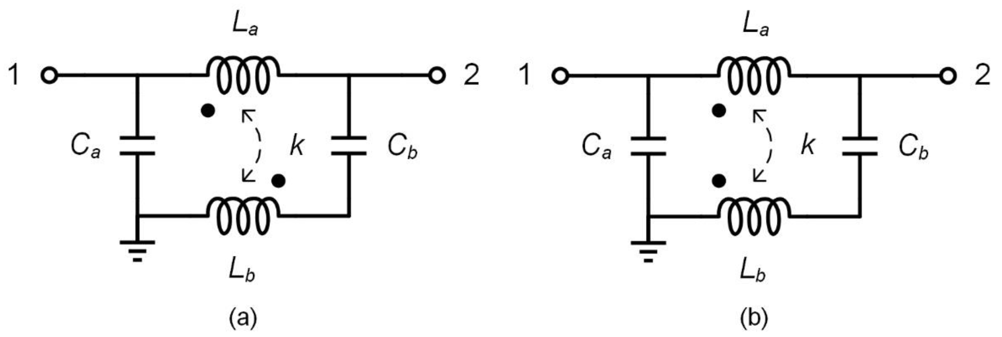
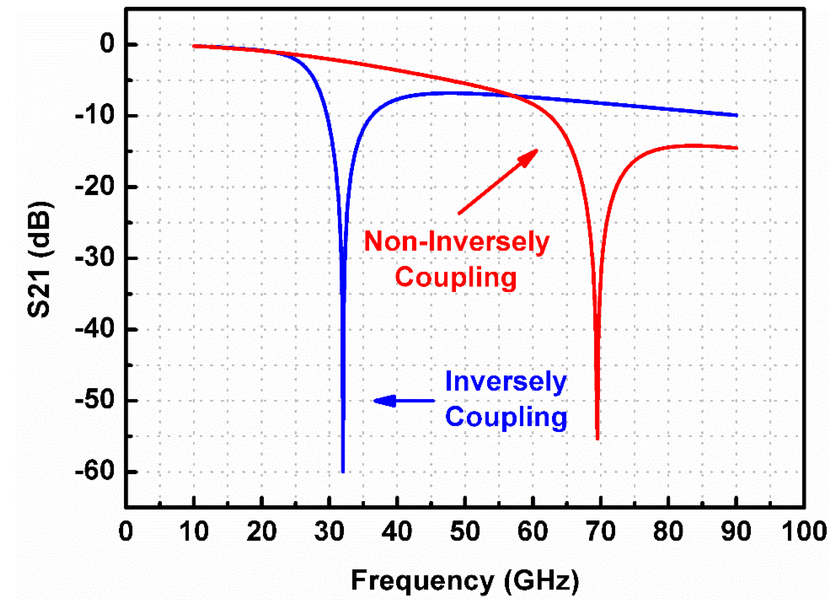
2.1. Analysis of Coupled Transmission Lines Based Resonators

We begin our proposed design by examining two coupled transmission lines based resonators as shown in Figure 2a,b by using lumped components formed models. La and Lb denote the inductance of the transmission lines and k is the mutual coupling factor between the metal trances. Ca and Cb represent the parasitic capacitance within the transmission lines and port 1 and 2 are the input and output nodes, respectively.
In order to calculate their resonance frequencies without considering the impedance matching network effect, the output port is assumed to be an open circuit [20]. The input admittance of the schematic illustrated in Figure 2a can be calculated as:
Y 1 = s C a [ s 2 ( L a + L b ) C a C b + 2 s 2 k L a L b C a C b + C a + C b ] s 2 ( L a + L b ) C a C b + 2 s 2 k L a L b C a C b + C a
where s = jω denotes the Laplace transform factor. Therefore, the resonance frequency (transmission zero frequency) can be obtained by making the imaginary part of Y1 to be zero:
ω 1 = C a + C b ( L a + L b + 2 k L a L b ) C a C b
Repeating the same process, the input admittance of the schematic shown in Figure 2b can be calculated as well:
Y 2 = s C a [ s 2 ( L a + L b ) C a C b 2 s 2 k L a L b C a C b + C a + C b ] s 2 ( L a + L b ) C a C b 2 s 2 k L a L b C a C b + C a
The resonance frequency (transmission zero frequency) of the non-inversely coupled transmission lines based resonator reflected in Figure 2b can be derived:
ω 2 = C a + C b ( L a + L b 2 k L a L b ) C a C b
which is higher than the frequency of the inversely coupling scheme as calculated in Equation (2). This is also verified by the simulation results shown in Figure 3 with La and Lb of 150 pH, Ca and Cb of 50 fF, and k value of 0.7. In other words, by adopting the inversely coupled transmission lines based resonator, the required transmission zero frequency can be implemented with a reduced area.

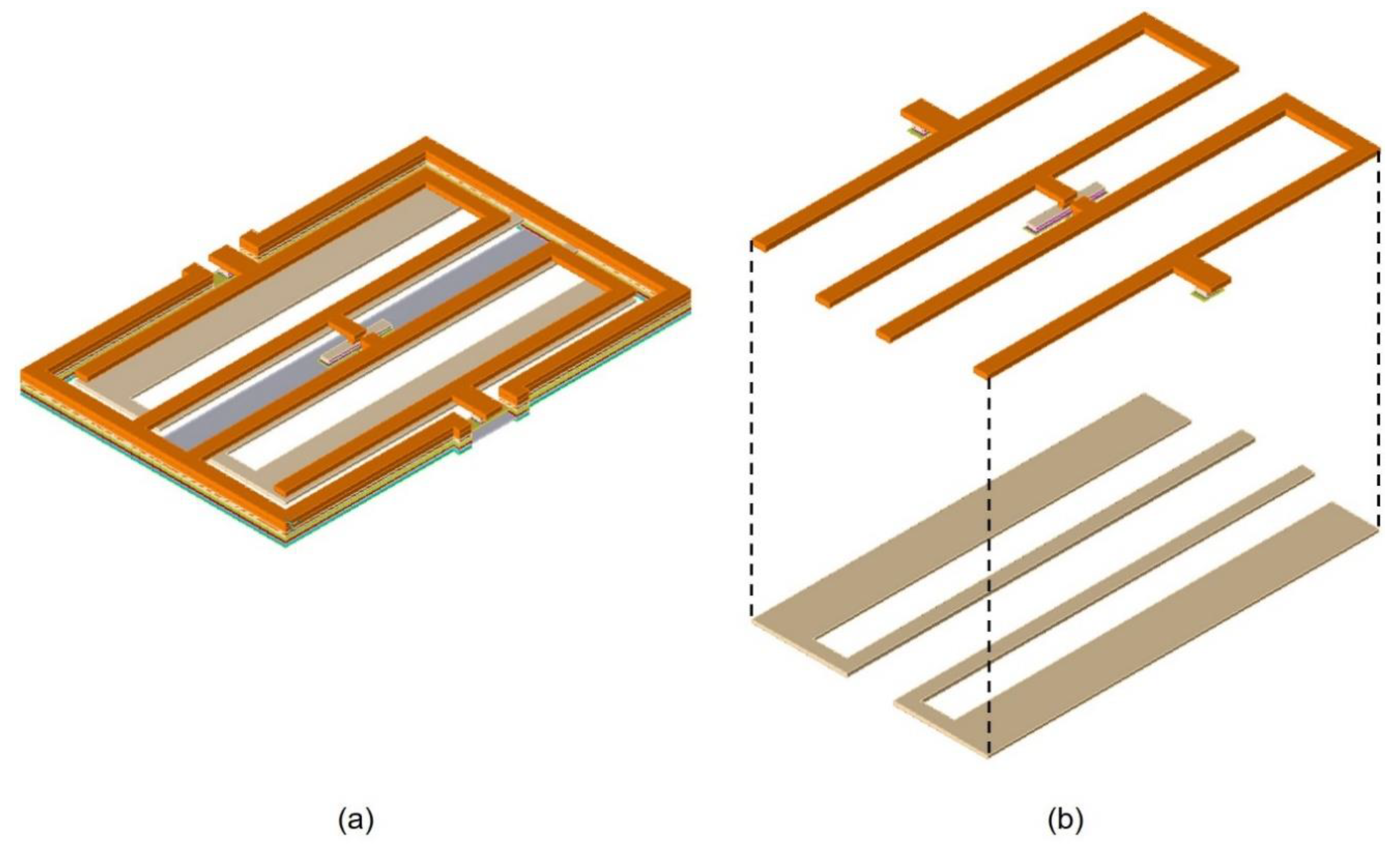
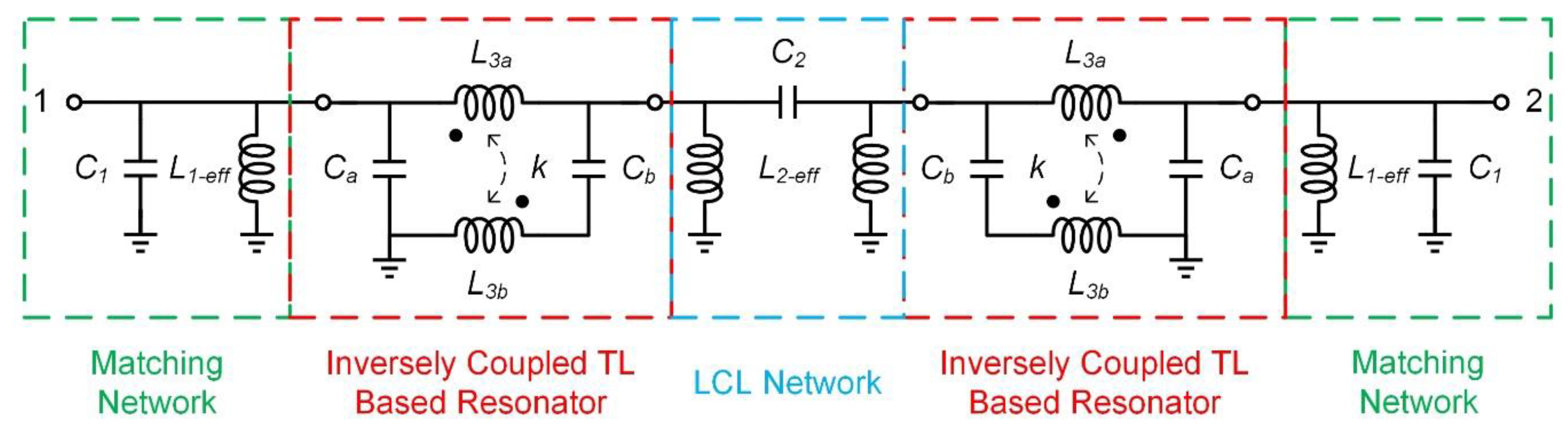
2.2. Proposed Bandpass Filter

To demonstrate how the inversely coupled transmission lines based resonator can be applied to our proposed design, please refer to the 3-D view of the proposed filter illustrated in Figure 4. The two topmost metals are adopted for the transmission line traces due to their relatively large thickness. The transmission lines are implemented by employing a U-shaped structure, which are stacked in alignment with each other to achieve a tight coupling factor.
To better understand the operation principle of the proposed BPF, the equivalent circuit model using lumped components is plotted in Figure 5 with the top views of the patterns on top metal 1 and 2 illustrated in Figure 6.
It can be seen that to further utilize the metal traces to save die area, the U-shaped transmission lines on the top metal 1 and 2 are divided into three sections, namely L1a, L2a, L3a and L1b, L2b, L3b, respectively. The coupled L1a and L1b together form an effective L1-eff, which can be found in Figure 5, and serve as a part of the impedance matching network. The effective inductor L2-eff, which consists of coupled L2a and L2b, can be employed to form an L-C-L π-type network with C2 to realize the first transmission zero. Besides, the L3a and L3b with their parasitic coupling capacitance form the inversely coupled transmission line resonator so that the second transmission zero can be obtained. Therefore, a Ka-band BPF can be implemented by choosing proper transmission zero frequencies. Although each transmission line pattern shown in Figure 6 has its own length and width, it will lead to a very complex optimization procedure, if we try to adjust them one by one. Instead, four parameters, W1, W2, W3, and W4, can be defined in the view of independent freedom degrees. It is evident that the required specifications of the designed BPF can be achieved by adjusting these four parameters. In addition, the coupling factor k in Figure 2 is inherently pre-determined by the process metal stack and shall not be discussed here.

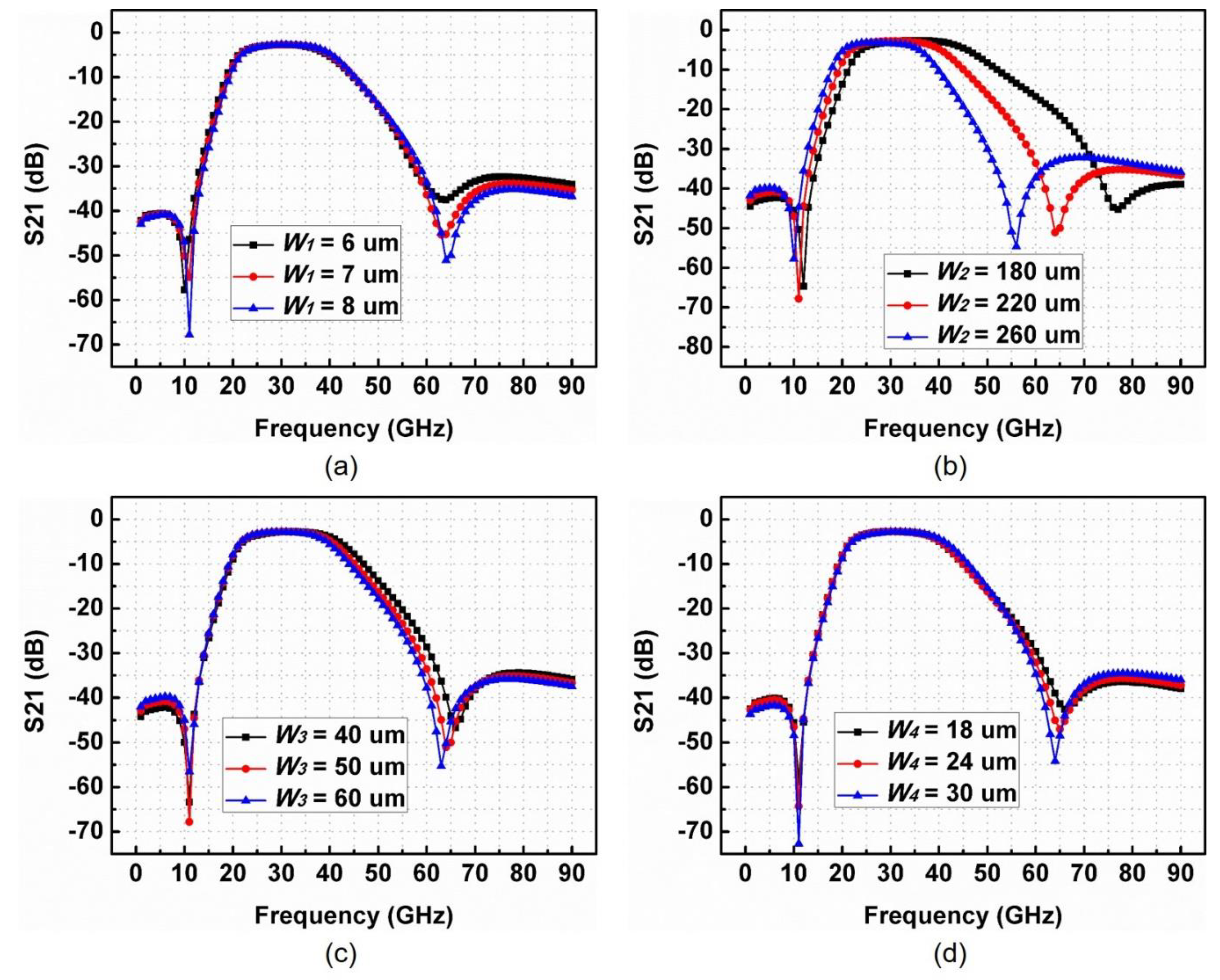
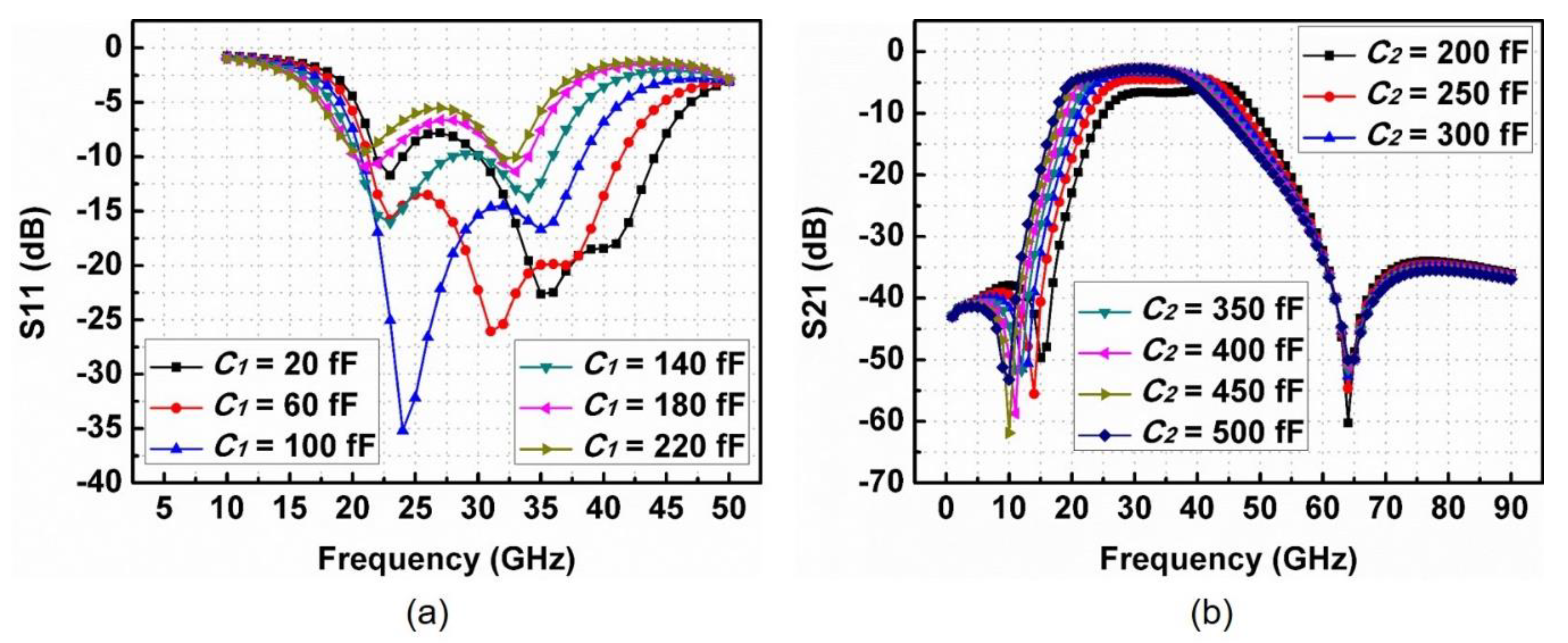
2.3. Case Studies of the Designed BPF

In this section, the four parameters will be studied in detail to demonstrate how they could influence the transmission zero of the proposed BPF. Figure 7 shows the insertion loss variations (S21) as the values of W1, W2, W3, and W4 are changed. Since a small value of W1 could result in an increased inductance of the associated transmission line as well as a large value of W2 and W3, the corresponded transmission zero will be decreased according to Equation (2), which is also proven by the simulation in Figure 7. Besides, a wide W4 indicates an enhanced fringed capacitance, which further decreases the transmission zero frequency.
It can also be observed that changing the value of W1 only influences the upper stopband transmission zero to a restricted limit but it mainly has an impact on the suppression, while W2 is the only parameter that can coarsely tune the frequency. Furthermore, the variation of W3 and W4 could lead to a fine-tuning of the second transmission zero frequency as indicated in Figure 7c,d. In general, the adjustment of W4 is preferred since it would help to save the overall area due to their stacked topology.
In order to tune the impedance matching and the first transmission zero frequency, the capacitances of C1 and C2 can be varied, as plotted in Figure 8. It can be seen that C1 dominates the impedance matching at both the input and output of the proposed BPF, while the selection of C2 determines the lower stopband frequency. Please note that under different values of C2, the insertion loss varies within a relatively large range. Therefore, the choice of C2 must be optimized in coordination with the optimization of W1, W2, W3. and W4. Although changing the values of W1, W2, W3, and W4 could certainly affect the impedance matching and the lower stopband frequency, the capacitance values of C1 and C2 could be overwhelmed and thus be regarded as the dominant components in determining the matching network as well as the first transmission zero point.
In summary, in order to implement the proposed BPF with required specifications, the value of W2 should be firstly chosen to place the second transmission zero approximately around the required upper stopband frequency. Thereafter, the widths of W3 and W4 should be selected to fine-tune the frequency. Besides, the width of W1 should be determined so that it is capable of carrying out the current based on the signal power target. Lastly, the values of C1 and C2 should be decided according to the required impedance matching and the lower stopband frequency. In our proposed design, all these parameters are optimized simultaneously by using Keysight Momentum simulation and the values of W1, W2, W3, W4, C1, and C2 are 8 μm, 233 μm, 56 μm, 28 μm, 83 fF, and 380 fF, respectively. The lower stopband frequency is around 11 GHz, while the upper stopband frequency is about 64 GHz.

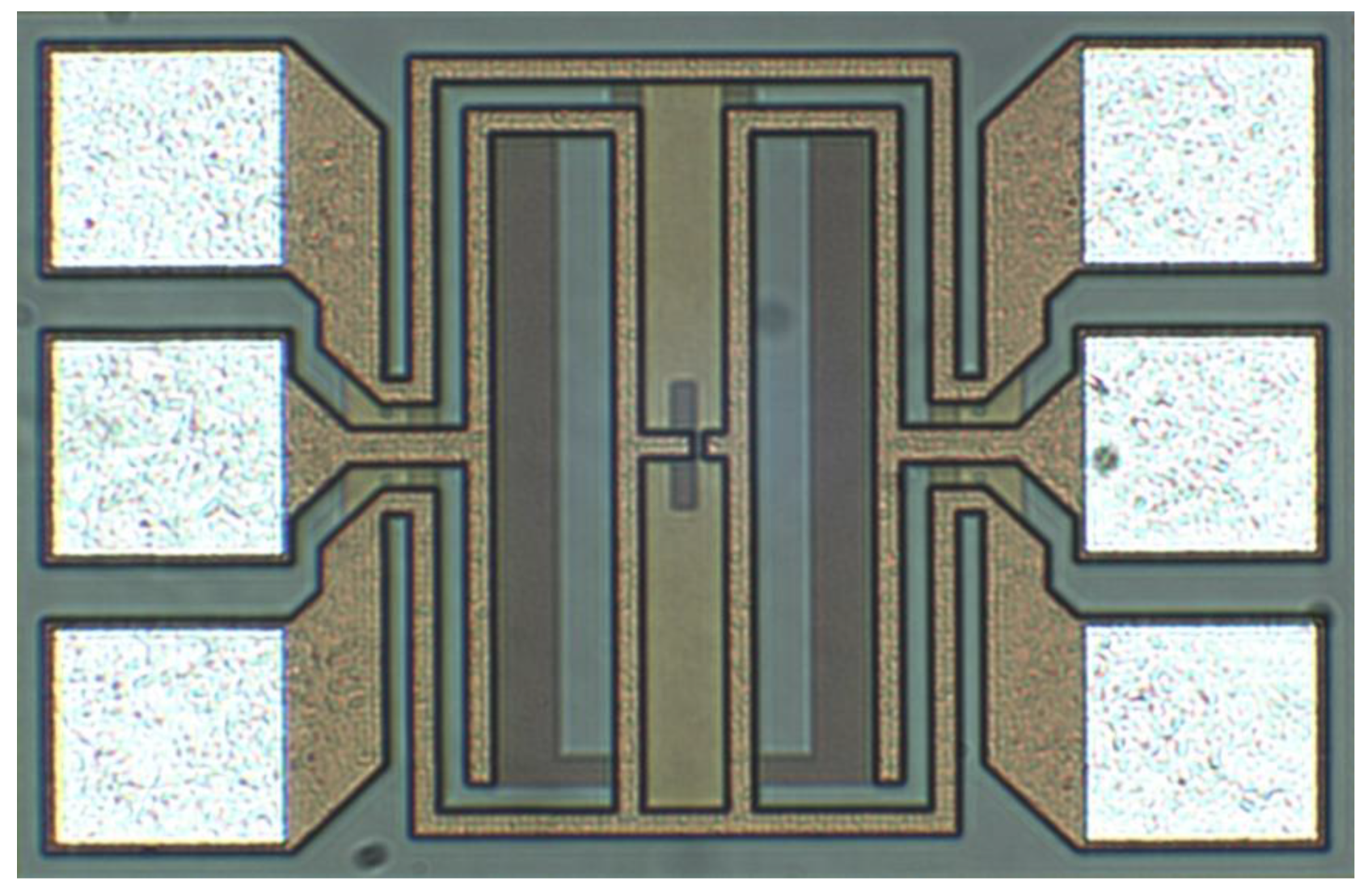
3. Experimental Results

The proposed BPF is fabricated in a commercial 0.13-μm SiGe BiCMOS process. Besides the two top metal traces, the capacitor in the proposed filter is also implemented in a metal-insulator-metal capacitor (MIMCAP) form, which make use of the silicon nitride layer provided by the process. The die microphotograph is shown in Figure 9 and the overall chip size is 176 × 269 μm2 excluding the test pads. The chip is measured on a probe station using Keysight N5247A vector network analyzer (VNA) as illustrated in Figure 10.
The measured results are plotted in Figure 11. The proposed filter achieves a minimum insertion loss of 3.6 dB at the frequency of 28.75 GHz. The measured bandwidth from 20.75 GHz to 41 GHz is at a fractional bandwidth of 65.6%, which is the second highest among all reported works as shown in Table 1. The return loss is better than −10 dB from 20.5 GHz to 39 GHz. In addition, the first transmission zero is located at 11.75 GHz with a suppression of 54 dB and the second transmission zero is around 67 GHz with the suppression of 34.6 dB. The measurement agrees conclusively with the simulation results as suggested in Figure 11.
Table 1 summaries the performance compared to other state-of-the-art works. It can be concluded that our proposed BPF achieves a very good performance among the state-of-the-art designs.

4. Conclusions

A novel Ka-band miniaturized bandpass filter with broad bandwidth is demonstrated by using inversely coupling U-shape transmission lines in this work. In the proposed filter, two transmission zeros can be generated using a cascaded U-shaped structure and it can also be proven that, by inversely coupling two stacked U-shaped transmission lines, the notch frequency at the upper stopband can be shifted to a lower frequency, which results in a more compact design. The key parameters affecting the performance of the proposed filter are investigated in detail with the effective lumped-circuit model. Fabricated in a 0.13 μm SiGe BiCMOS process, our proposed filter achieves a minimum insertion loss of 3.6 dB at a frequency of 28.75 GHz and the measured bandwidth is from 20.75 GHz to 41 GHz. The return loss is better than −10 dB from 20.5 GHz to 39 GHz. The lower stopband frequency is located at 11.75 GHz with a suppression of 54 dB and the upper stopband frequency is around 67 GHz with an attenuation of 34.6 dB. The measurement agrees very well with the simulation results and the overall chip size of the proposed filter is 176 × 269 μm2. Furthermore, our proposed design occupies a comparable area with most designs listed in the comparison table, which have a lower order. To achieve a similar level of out-of-band suppression, those designs need to cascade two lower-order filter cells together. Consequently, their physical sizes would become relatively large.

Author Contributions

Conceptualization, K.M.; methodology, K.M.; validation, K.M.; formal analysis, K.M.; writing—original draft preparation, K.M.; writing—review and editing, H.L.; supervision, K.S.Y.; funding acquisition, K.S.Y. All authors have read and agreed to the published version of the manuscript.

Funding

This research was funded by Singapore National Research Foundation, award number NRF-CRP20-2017-0003 and project number CRP20-2017-0006.

Acknowledgments

The author would like to acknowledge the IHP microelectronics for the circuit fabrication.

Conflicts of Interest

The authors declare no conflict of interest.

References

  1. Zhang, W.; Yao, Z.; Zhang, J.; Kim, E.-S.; Kim, N.-Y. A Compact Dual-Mode Bandpass Filter with High Out-of-Band Suppression Using a Stub-Loaded Resonator Based on the GaAs IPD Process. Electronics 2020, 9, 712. [Google Scholar] [CrossRef]
  2. Zhang, P.; Liu, L.; Chen, D.; Weng, M.-H.; Yang, R.-Y. Application of a Stub-Loaded Square Ring Resonator for Wideband Bandpass Filter Design. Electronics 2020, 9, 176. [Google Scholar] [CrossRef] [Green Version]
  3. Weng, M.-H.; Zheng, F.-Z.; Lai, H.-Z.; Liu, S.-K. Compact Ultra-Wideband Bandpass Filters Achieved by Using a Stub-Loaded Stepped Impedance Resonator. Electronics 2020, 9, 209. [Google Scholar] [CrossRef] [Green Version]
  4. Liu, L.; Zhang, P.; Weng, M.-H.; Tsai, C.-Y.; Yang, R.-Y. A Miniaturized Wideband Bandpass Filter Using Quarter-Wavelength Stepped-Impedance Resonators. Electronics 2019, 8, 1540. [Google Scholar] [CrossRef] [Green Version]
  5. Hou, Z.; Liu, C.; Zhang, B.; Song, R.; Wu, Z.; Zhang, J.; He, D. Dual-/Tri-Wideband Bandpass Filter with High Selectivity and Adjustable Passband for 5G Mid-Band Mobile Communications. Electronics 2020, 9, 205. [Google Scholar] [CrossRef] [Green Version]
  6. Chen, W.-Z.; Chen, W.-H.; Hsu, K.-C. Three-Dimensional Fully Symmetric Inductors, Transformer, and Balun in CMOS Technology. IEEE Trans. Circuits Syst. I Regul. Pap. 2007, 54, 1413–1423. [Google Scholar] [CrossRef] [Green Version]
  7. Chirala, M.; Guan, X.; Nguyen, C. Integrated Multilayered On-Chip Inductors for Compact CMOS RFICs and Their Use in a Miniature Distributed Low-Noise-Amplifier Design for Ultra-Wideband Applications. IEEE Trans. Microw. Theory Tech. 2008, 56, 1783–1789. [Google Scholar] [CrossRef]
  8. Chang, S.-C.; Chen, Y.; Chang, S.-F.; Jeng, Y.-H.; Wei, C.-L.; Huang, C.-H.; Jeng, C.-P. Compact Millimeter-Wave CMOS Bandpass Filters Using Grounded Pedestal Stepped-Impedance Technique. IEEE Trans. Microw. Theory Tech. 2010, 58, 3850–3858. [Google Scholar] [CrossRef]
  9. Lin, Y.-S.; Nguyen, V.K. 94-GHz CMOS Power Amplifiers Using Miniature Dual Y-Shaped Combiner With RL Load. IEEE Trans. Circuits Syst. I Regul. Pap. 2017, 64, 1–14. [Google Scholar] [CrossRef]
  10. Lai, I.C.H.; Kambayashi, Y.; Fujishima, M. 60-GHz CMOS Down-Conversion Mixer with Slow-Wave Matching Transmission Lines. In Proceedings of the 2006 IEEE Asian Solid-State Circuits Conference; Institute of Electrical and Electronics Engineers, China, Hangzhou, 13–15 November 2006. [Google Scholar]
  11. Franc, A.-L.; Pistono, E.; Meunier, G.; Gloria, D.; Ferrari, P. A Lossy Circuit Model Based on Physical Interpretation for Integrated Shielded Slow-Wave CMOS Coplanar Waveguide Structures. IEEE Trans. Microw. Theory Tech. 2012, 61, 754–763. [Google Scholar] [CrossRef]
  12. Mahmoud, N.; Barakat, A.; Abdel-Rahman, A.B.; Allam, A.; Pokharel, R.K. Compact Size On-Chip 60 GHz H-Shaped Resonator BPF. IEEE Microw. Wirel. Components Lett. 2016, 26, 681–683. [Google Scholar] [CrossRef]
  13. El-Hameed, A.S.A.; Barakat, A.; Abdel-Rahman, A.B.; Allam, A.; Pokharel, R.K. Ultracompact 60-GHz CMOS BPF Employing Broadside-Coupled Open-Loop Resonators. IEEE Microw. Wirel. Components Lett. 2017, 27, 818–820. [Google Scholar] [CrossRef]
  14. Yang, Y.; Zhu, X.; Xue, Q. Design of an Ultracompact On-Chip Bandpass Filter Using Mutual Coupling Technique. IEEE Trans. Electron. Devices 2018, 65, 1087–1093. [Google Scholar] [CrossRef]
  15. Yang, Y.; Zhu, H.; Zhu, X.; Xue, Q. A Low-Loss Bandpass Filter using Edge-Coupled Resonator With Capacitive Feeding in (Bi)-CMOS Technology. IEEE Electron. Device Lett. 2018, 39, 787–790. [Google Scholar] [CrossRef]
  16. Zhu, H.; Yang, Y.; Zhu, X.; Sun, Y.; Wong, S.-W. Miniaturized Resonator and Bandpass Filter for Silicon-Based Monolithic Microwave and Millimeter-Wave Integrated Circuits. IEEE Trans. Circuits Syst. I: Regul. Pap. 2018, 65, 4062–4071. [Google Scholar] [CrossRef] [Green Version]
  17. Hou, Z.J.; Yang, Y.; Zhu, X.; Li, Y.C.; Dutkiewicz, E.; Xue, Q. A Compact and Low-Loss Bandpass Filter Using Self-Coupled Folded-Line Resonator With Capacitive Feeding Technique. IEEE Electron. Device Lett. 2018, 39, 1. [Google Scholar] [CrossRef]
  18. Zhu, H.; Zhu, X.; Yang, Y.; Xue, Q. Design of Wideband Third-Order Bandpass Filters Using Broadside-Coupled Resonators in 0.13-μm (Bi)-CMOS Technology. IEEE Trans. Microw. Theory Tech. 2018, 66, 5593–5604. [Google Scholar] [CrossRef]
  19. Li, M.; Yang, Y.; Xu, K.; Zhu, X.; Wong, S.-W. Microwave On-Chip Bandpass Filter Based on Hybrid Coupling Technique. IEEE Trans. Electron. Devices 2018, 65, 5453–5459. [Google Scholar] [CrossRef]
  20. Bautista, M.G.; Zhu, H.; Zhu, X.; Yang, Y.; Sun, Y.; Dutkiewicz, E. Compact Millimeter-Wave Bandpass Filters Using Quasi-Lumped Elements in 0.13-μm (Bi)-CMOS Technology for 5G Wireless Systems. IEEE Trans. Microw. Theory Tech. 2019, 67, 3064–3073. [Google Scholar] [CrossRef] [Green Version]
  21. Sun, F.; Zhu, H.; Zhu, X.; Yang, Y.; Sun, Y.; Zhang, X. Design of Millimeter-Wave Bandpass Filters With Broad Bandwidth in Si-Based Technology. IEEE Trans. Electron. Devices 2019, 66, 1174–1181. [Google Scholar] [CrossRef]
  22. Zhu, H.; Zhu, X.; Yang, Y.; Sun, Y. Design of Miniaturized On-Chip Bandpass Filters Using Inverting-Coupled Inductors in (Bi)-CMOS Technology. IEEE Trans. Circuits Syst. I Regul. Pap. 2019, 67, 647–657. [Google Scholar] [CrossRef]
  23. Sun, F.; Zhu, H.; Zhu, X.; Yang, Y.; Gomez-Garcia, R. Design of On-Chip Millimeter-Wave Bandpass Filters Using Multilayer Patterned-Ground Element in 0.13-μm (Bi)-CMOS Technology. IEEE Trans. Microw. Theory Tech. 2019, 67, 5159–5170. [Google Scholar] [CrossRef]
  24. Chakraborty, S.; Yang, Y.; Zhu, X.; Sevimli, O.; Xue, Q.; Esselle, K.P.; Heimlich, M. A Broadside-Coupled Meander-Line Resonator in 0.13-μm SiGe Technology for Millimeter-Wave Application. IEEE Electron. Device Lett. 2016, 37, 329–332. [Google Scholar] [CrossRef]
  25. Zhong, Y.; Yang, Y.; Zhu, X.; Dutkiewicz, E.; Shum, K.M.; Yang, Y. An On-Chip Bandpass Filter Using a Broadside-Coupled Meander Line Resonator with a Defected-Ground Structure. IEEE Electron. Device Lett. 2017, 38, 626–629. [Google Scholar] [CrossRef]
  26. Weng, M.-H.; Hsu, C.-W.; Lan, S.-W.; Yang, R.-Y. An Ultra-Wideband Bandpass Filter with a Notch Band and Wide Upper Bandstop Performances. Electronics 2019, 8, 1316. [Google Scholar] [CrossRef] [Green Version]
  27. Yang, Y.; Liu, H.; Hou, Z.J.; Zhu, X.; Dutkiewicz, E.; Yang, Y. Compact On-Chip Bandpass Filter With Improved In-Band Flatness and Stopband Attenuation in 0.13-μm (Bi)-CMOS Technology. IEEE Electron. Device Lett. 2017, 38, 1359–1362. [Google Scholar] [CrossRef]
Figure 1. Illustration of how to form a passband by using two transmission zeros.
Electronics 09 01608 g001
Figure 2. (a) Inversely and (b) non-inversely coupled transmission lines based resonators.
Electronics 09 01608 g002
Figure 3. Simulated transmission zeros with inversely and non-inversely coupled transmission lines based resonators.
Electronics 09 01608 g003
Figure 4. Layout of (a) proposed filter, (b) two topmost metal traces without ground.
Electronics 09 01608 g004
Figure 5. Equivalent circuits for the structure presented in Figure 4.
Electronics 09 01608 g005
Figure 6. Top view of the patterns on (a) top metal 1, (b) top metal 2.
Electronics 09 01608 g006
Figure 7. Insertion loss under different values of (a) W1, (b) W2, (c) W3, (d) W4.
Electronics 09 01608 g007
Figure 8. (a) S11 variation under different values of C1, (b) S21 variation under different values of C2.
Electronics 09 01608 g008
Figure 9. Die microphotograph of the proposed bandpass filters (BPF).
Electronics 09 01608 g009
Figure 10. Measurement setup for the proposed BPF.
Electronics 09 01608 g010
Figure 11. Measured and simulated results of the proposed BPF.
Electronics 09 01608 g011
Table 1. Performance summary and comparison with other published works.
Ref.Center Frequency (GHz)Insertion Loss (dB)Fractional Bandwidth (%)Suppression at Lower Stopband (dB)Suppression at Upper Stopband (dB)Area (mm2)
[15]351.721.9N.A.200.039
[17]301.6623.4N.A.25.40.009
[18]313.951N.A.450.075
[19]26.53.850.9N.A.360.176
[20]293.526.747240.028
[21]26.62.67045320.066
[23]313.211.4>25>250.024
[23]312.717.5>25>250.044
[24]312.423N.A.200.024
[25]332.618N.A.440.038
This Work30.83.665.65434.60.047

