Effect of Annealing Environment on the Performance of Sol–Gel-Processed ZrO2 RRAM

 ,
,  ,
,  and
and 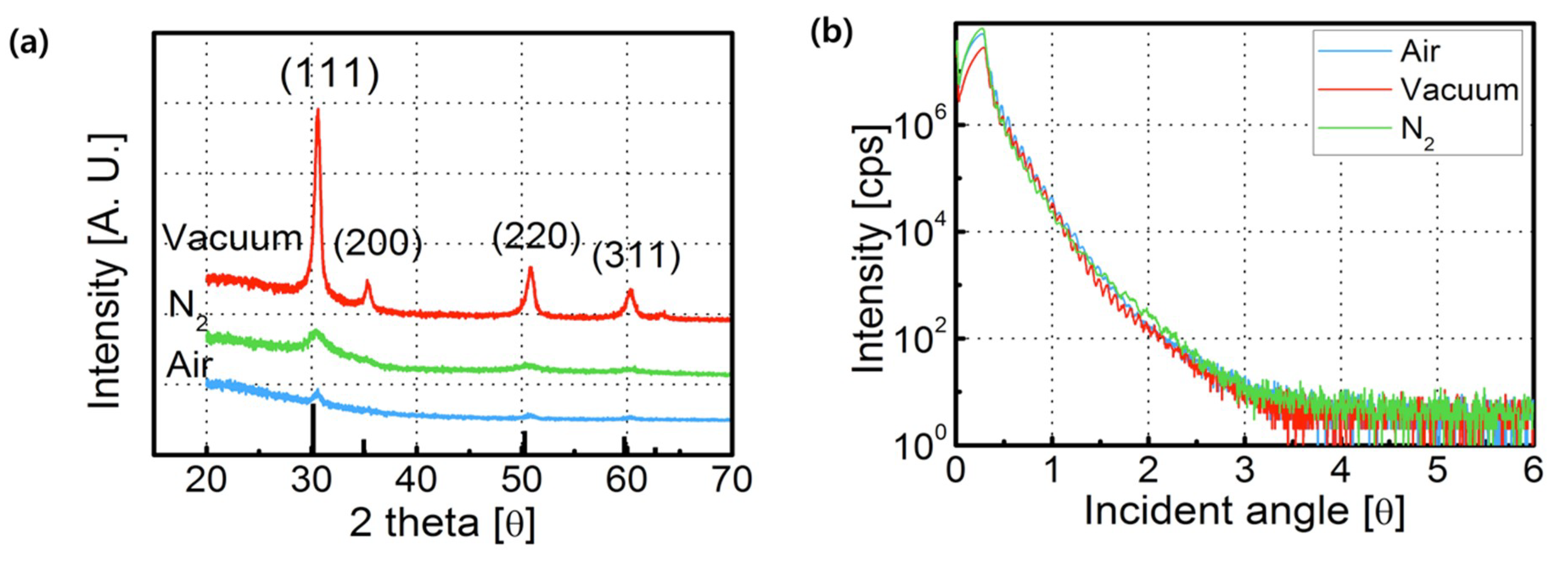
Abstract
:1. Introduction
2. Materials and Methods
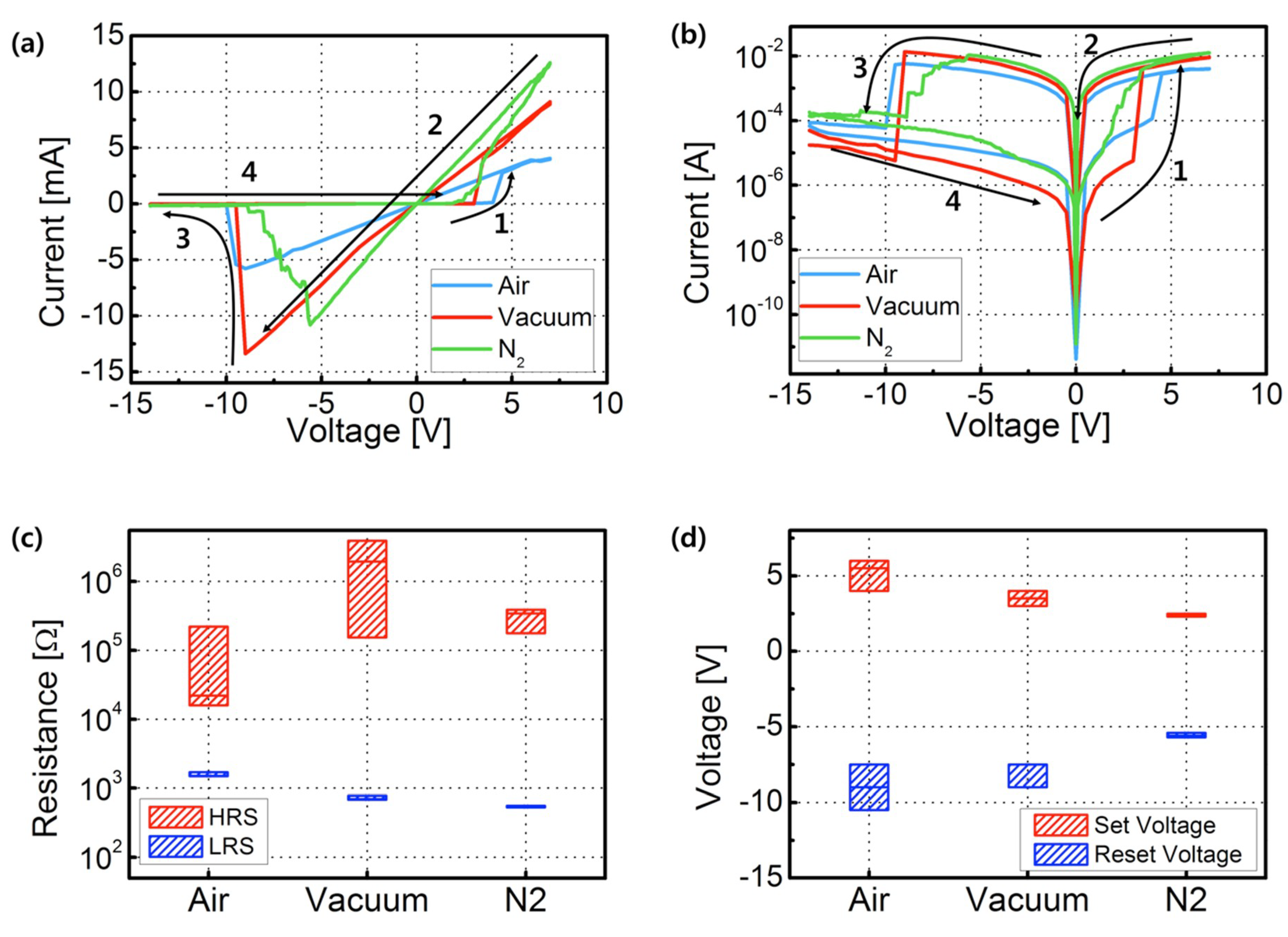
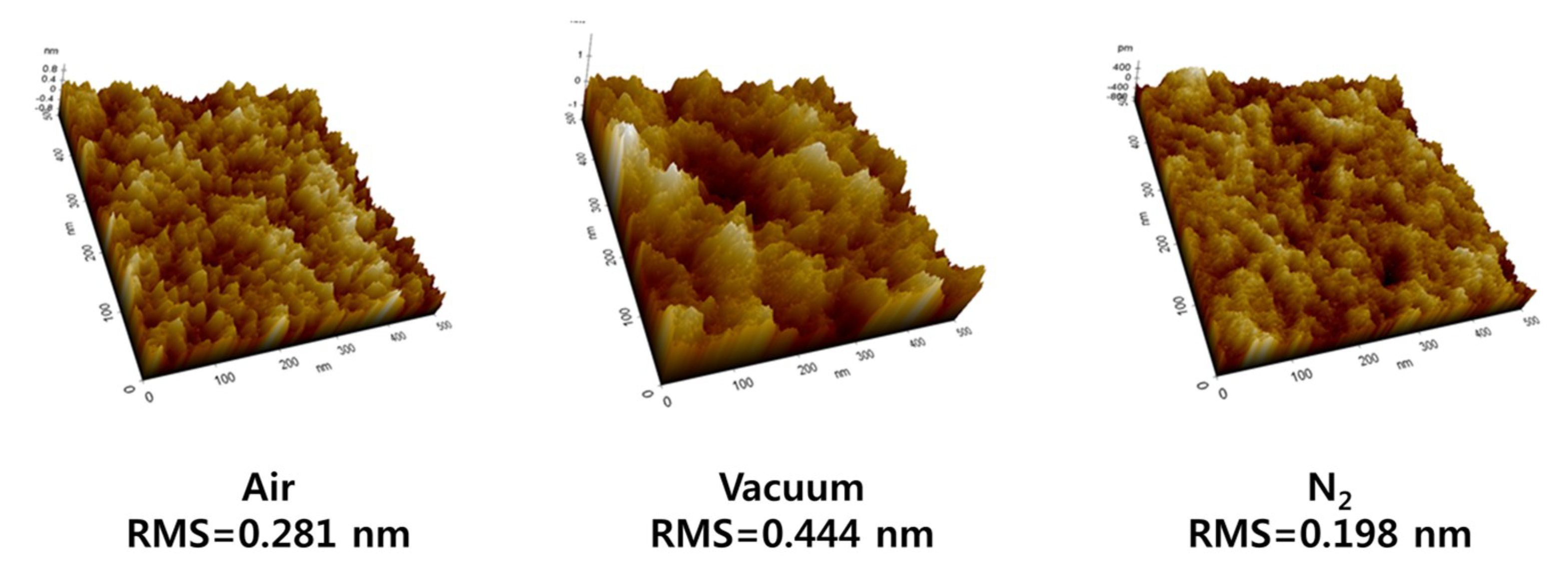
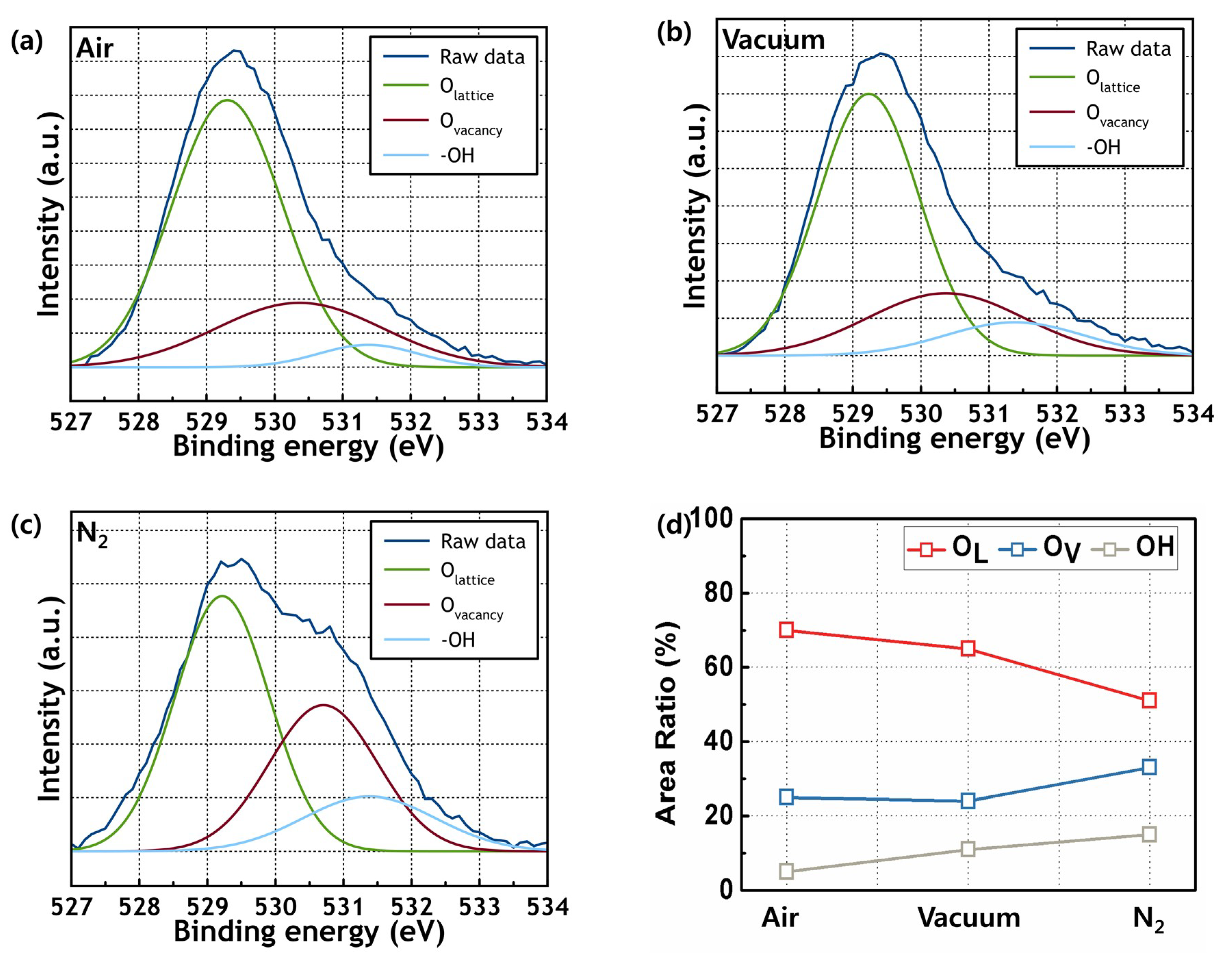
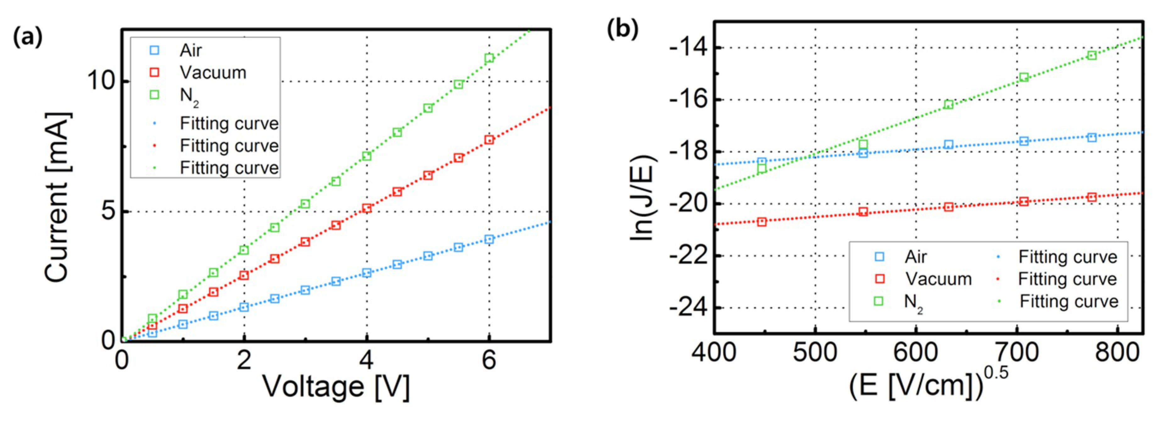
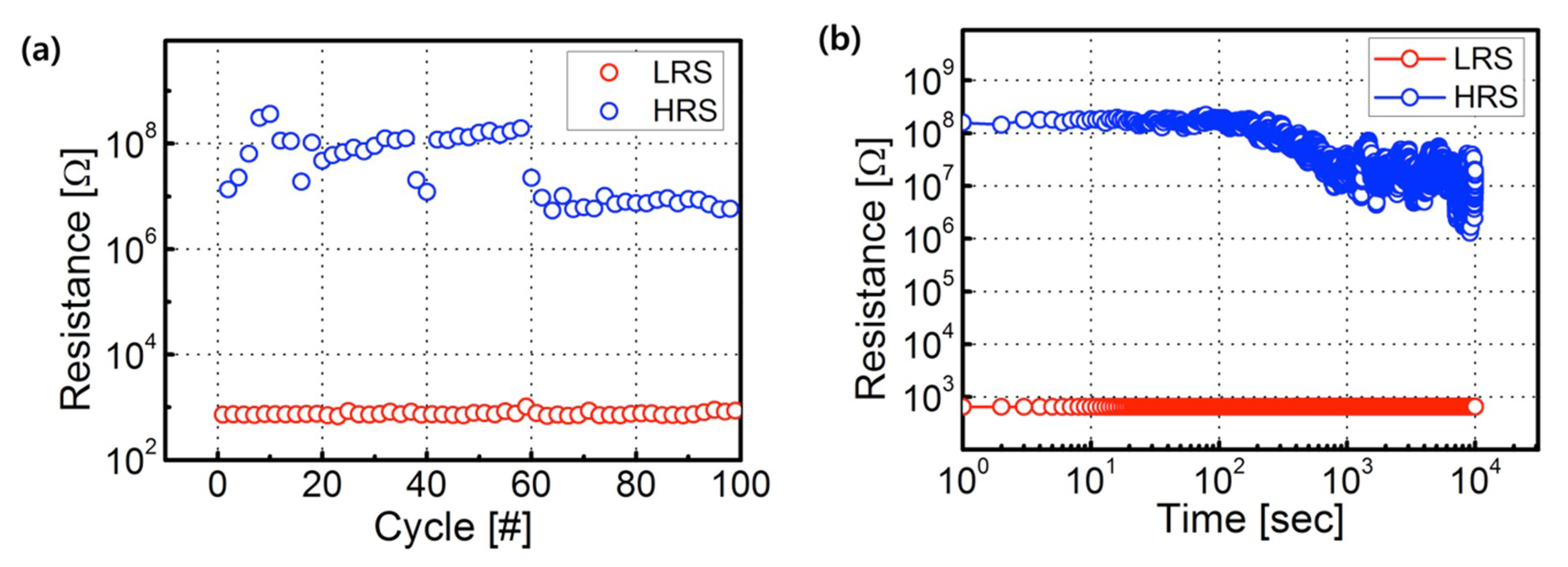
3. Results and Discussion
4. Conclusions
Author Contributions
Funding
Conflicts of Interest
References
- Li, Y.; Long, S.; Zhang, M.; Liu, Q.; Shao, L.; Zhang, S.; Wang, Y.; Zuo, Q.; Liu, S.; Liu, M. Resistive switching properties of Au/ZrO2/Ag structure for low-voltage nonvolatile memory applications. IEEE Electron Device Lett. 2010, 31, 117–119. [Google Scholar]
- Puglisi, F.M.; Larcher, L.; Bersuker, G.; Padovani, A.; Pavan, P. An empirical model for RRAM resistance in low- and high-resistance states. IEEE Electron Device Lett. 2013, 34, 387–389. [Google Scholar] [CrossRef]
- Chang, K.C.; Tsai, T.M.; Chang, T.C.; Wu, H.H.; Chen, J.H.; Syu, Y.E.; Chang, G.W.; Chu, T.J.; Liu, G.R.; Su, Y.T.; et al. Characteristics and mechanisms of silicon-oxide-based resistance random access memory. IEEE Electron Device Lett. 2013, 34, 399–401. [Google Scholar] [CrossRef]
- Song, S.; Cho, B.; Kim, T.W.; Ji, Y.; Jo, M.; Wang, G.; Choe, M.; Kahng, Y.H.; Hwang, H.; Lee, T. Three-dimensional integration of organic resistive memory devices. Adv. Mater. 2010, 22, 5048–5052. [Google Scholar] [CrossRef] [PubMed]
- Zhuge, F.; Peng, S.; He, C.; Zhu, X.; Chen, X.; Liu, Y.; Li, R.W. Improvement of resistive switching in Cu/ZnO/Pt sandwiches by weakening the randomicity of the formation/rupture of Cu filaments. Nanotechnology 2011, 22, 275204. [Google Scholar] [CrossRef] [PubMed]
- Jang, J.; Pan, F.; Braam, K.; Subramanian, V. Resistance switching characteristics of solid electrolyte chalcogenide Ag2Se nanoparticles for flexible nonvolatile memory applications. Adv. Mater. 2012, 24, 3573–3576. [Google Scholar] [CrossRef]
- Jang, J. Effect of electrode material on characteristics of non-volatile resistive memory consisting of Ag2S nanoparticles. AIP Adv. 2016, 6, 075006. [Google Scholar] [CrossRef]
- Jang, J.; Subramanian, V. Effect of electrode material on resistive switching memory behavior of solution-processed resistive switches: Realization of robust multi-level cells. Thin Solid Films. 2017, 625, 87–92. [Google Scholar] [CrossRef]
- Lee, S.; Kim, T.; Jang, B.; Lee, W.Y.; Song, K.C.; Kim, H.S.; Do, S.Y.; Hwang, S.B.; Chung, S.; Jang, J. Impact of Device Area and Film Thickness on Performance of Sol-gel Processed ZrO2 RRAM. IEEE Electron Device Lett. 2018, 39, 668–671. [Google Scholar] [CrossRef]
- Jang, J.; Kitsomboonloha, R.; Swisher, S.L.; Park, E.S.; Kang, H.; Subramanian, V. Transparent high-performance thin film transistors from solution processed SnO2/ZrO2 gel-like precursors. Adv. Mater. 2013, 25, 1042–1047. [Google Scholar] [CrossRef] [PubMed]
- Jang, J.; Kang, H.; Chakravarthula, H.C.N.; Subramanian, V. Fully inkjet-printed transparent oxide thin film transistors using a fugitive wettability switch. Adv. Electron. Mater. 2015, 1, 1500086. [Google Scholar] [CrossRef]
- Kwon, H.J.; Jang, J.; Grigoropoulos, C.P. Laser Direct Writing Process for Making Electrodes and High-k Sol–Gel ZrO2 for Boosting Performances of MoS2 Transistors. ACS Appl. Mater. Interfaces 2016, 8, 9314–9318. [Google Scholar] [CrossRef] [PubMed]
- Chen, P.Y.; Yu, S. Impact of vertical RRAM device characteristics on 3D cross-point array design. In Proceedings of the 2014 IEEE 6th International Memory Workshop (IMW), Taipei, Taiwan, 18–21 May 2014. [Google Scholar]
- Zackriya, V.M.; Kittur, H.M.; Chin, A. A novel read scheme for large size on resistor resistive random access memory array. Sci. Rep. 2017, 7, 42375. [Google Scholar] [CrossRef] [PubMed]
- Khan, W.; Khan, F.; Ajmal, H.M.S.; Huda, N.U.; Kim, S.D. Evolution of structural and optical properties on ZrO2 nanorods grown on vacuum annealed seed crystallites. Nanomaterials 2018, 8, 68. [Google Scholar] [CrossRef] [PubMed]
- Dane, A.D.; Veldhuis, A.; de Boer, D.K.G.; Leenaers, A.J.G.; Buydens, L.M.C. Application of genetic algorithms for characterization of thin layered materials by glancing incidence X-ray reflectometry. Physica B 1998, 253, 254–268. [Google Scholar] [CrossRef]
- Cai, W.; Chu, Z.; Wei, J.; Fang, Z.; Ning, H.; Zheng, Z.; Zhou, S.; Yao, R.; Peng, J.; Lu, X. A simple method for high performance solution processed, amorphous ZrO2 gate insulator TFT with a high concentration precursors. Materials 2017, 10, 972. [Google Scholar] [CrossRef] [PubMed]
- Wei, X.; Hung, H.; Ye, C.; Wei, W.; Zhou, H.; Chen, Y.; Zhang, R.; Zhang, L.; Xia, Q. Exploring the role of nitrogen incorporation in ZrO2 resistive switching film for enhancing the device performance. J. Alloy. Compd. 2019, 755, 1301–1306. [Google Scholar] [CrossRef]
- Sze, S.M. Current transport and maximum dielectric strength of silicon nitride films. J. Appl. Phys. 1967, 38, 2951–2956. [Google Scholar] [CrossRef]
- Huang, R.; Yan, X.; Ye, S.; Kashtiban, R.; Beanland, R.; Morgan, K.A.; Charlton, M.D.B.; de Groot, C.H. Compliance-free ZrO2/ZrO2−x/ZrO2 resistive memory with controllable interfacial multistate switching behavior. Nanosc. Res. Lett. 2017, 12, 384. [Google Scholar] [CrossRef] [PubMed]
- Parreira, P.; Paterson, G.W.; McVitie, S.; MacLaren, D.A. Stability, bistability and instability of amorphous ZrO2 resistive memory devices. J. Phys. D Appl. Phys. 2016, 49, 095111. [Google Scholar] [CrossRef]


© 2019 by the authors. Licensee MDPI, Basel, Switzerland. This article is an open access article distributed under the terms and conditions of the Creative Commons Attribution (CC BY) license (http://creativecommons.org/licenses/by/4.0/).
Share and Cite
Ha, S.; Lee, H.; Lee, W.-Y.; Jang, B.; Kwon, H.-J.; Kim, K.; Jang, J. Effect of Annealing Environment on the Performance of Sol–Gel-Processed ZrO2 RRAM. Electronics 2019, 8, 947. https://doi.org/10.3390/electronics8090947
Ha S, Lee H, Lee W-Y, Jang B, Kwon H-J, Kim K, Jang J. Effect of Annealing Environment on the Performance of Sol–Gel-Processed ZrO2 RRAM. Electronics. 2019; 8(9):947. https://doi.org/10.3390/electronics8090947
Chicago/Turabian StyleHa, Seunghyun, Hyunjae Lee, Won-Yong Lee, Bongho Jang, Hyuk-Jun Kwon, Kwangeun Kim, and Jaewon Jang. 2019. "Effect of Annealing Environment on the Performance of Sol–Gel-Processed ZrO2 RRAM" Electronics 8, no. 9: 947. https://doi.org/10.3390/electronics8090947
APA StyleHa, S., Lee, H., Lee, W.-Y., Jang, B., Kwon, H.-J., Kim, K., & Jang, J. (2019). Effect of Annealing Environment on the Performance of Sol–Gel-Processed ZrO2 RRAM. Electronics, 8(9), 947. https://doi.org/10.3390/electronics8090947