A Nonisolated Three-Port DC–DC Converter with Continuous Input and Output Currents Based on Cuk Topology for PV/Fuel Cell Applications


Abstract
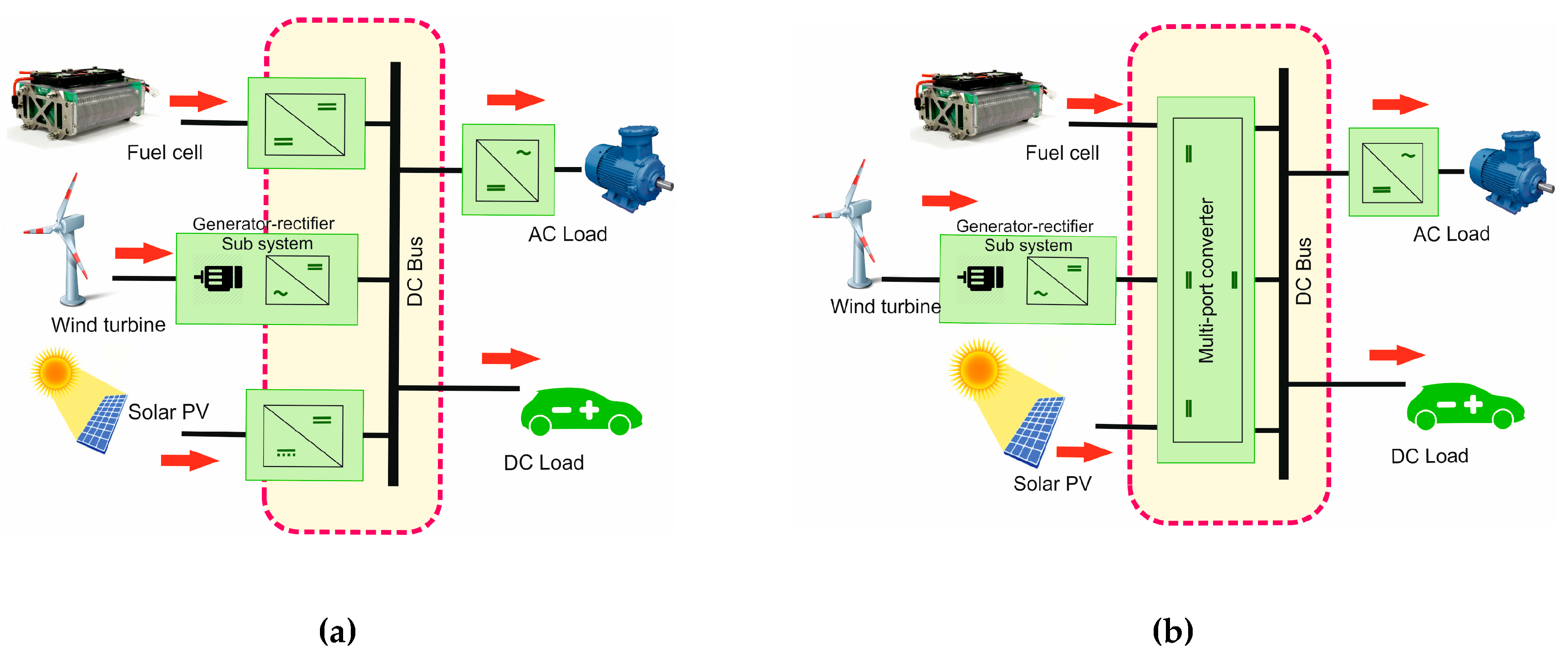
:1. Introduction
- Both the input ports share common output inductor, hence minimizing the component count.
- Continuous current with less ripple in all the ports (the input and output ports).
- Delivered power from each input can be independently controlled
- Buck–boost output voltages can be obtained.
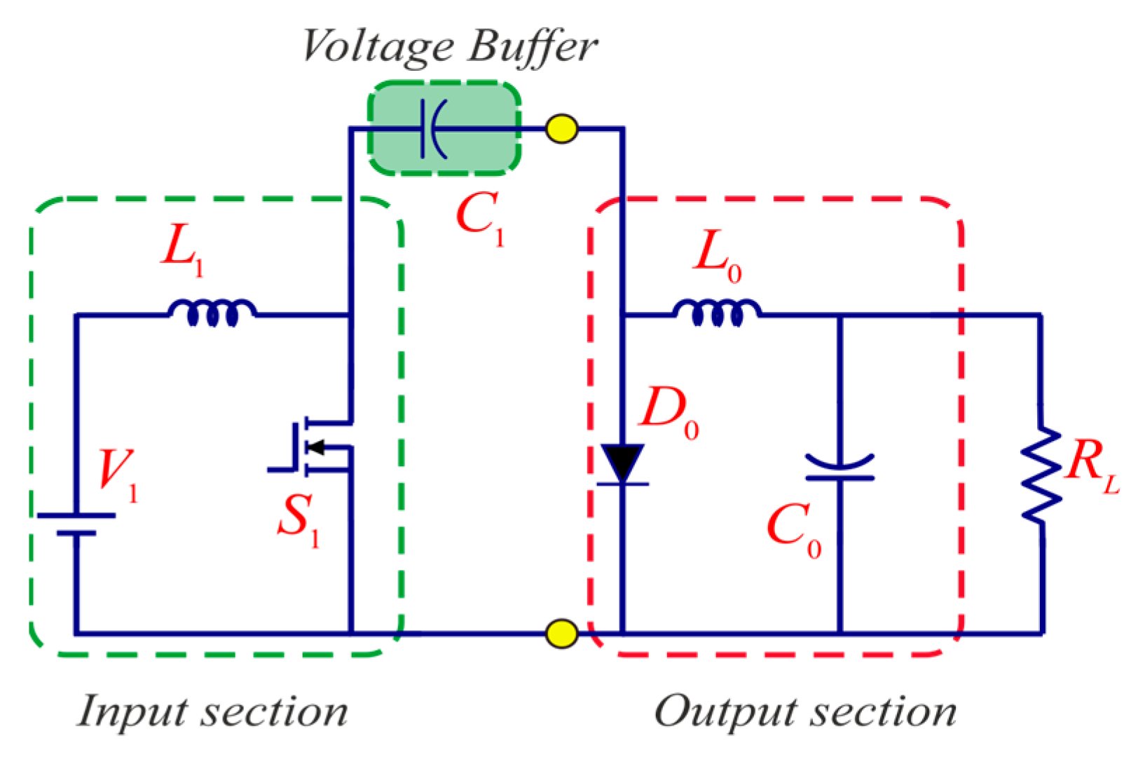
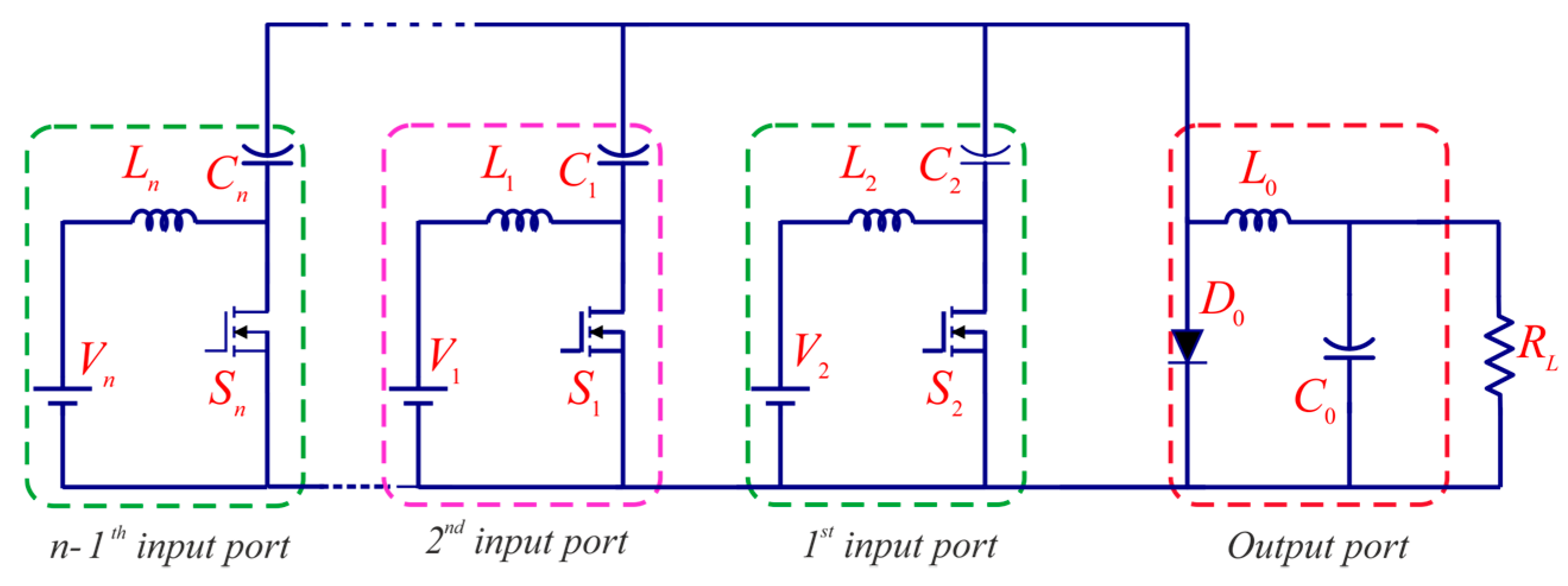
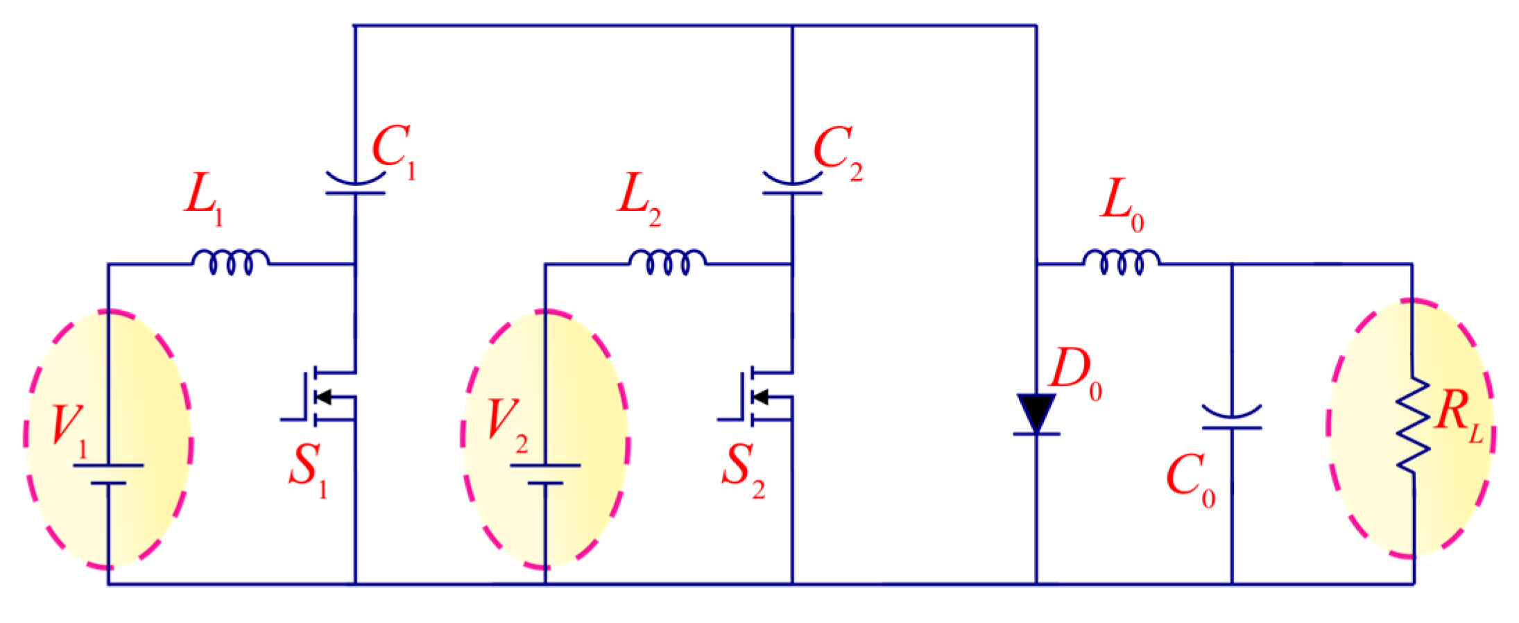
2. Proposed Converter Structure
2.1. Synthesis of the NI-TPC Converter
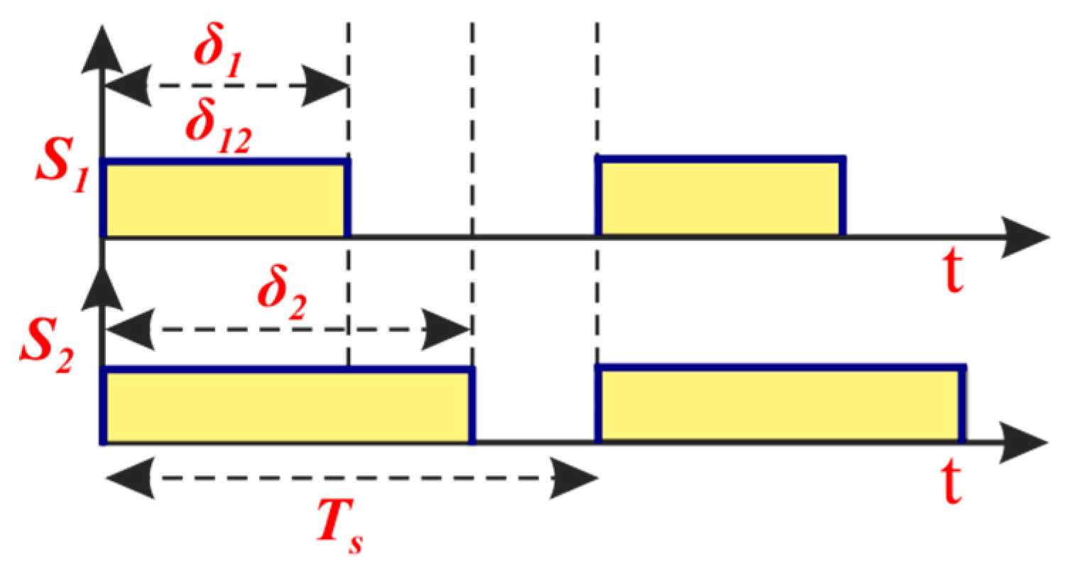
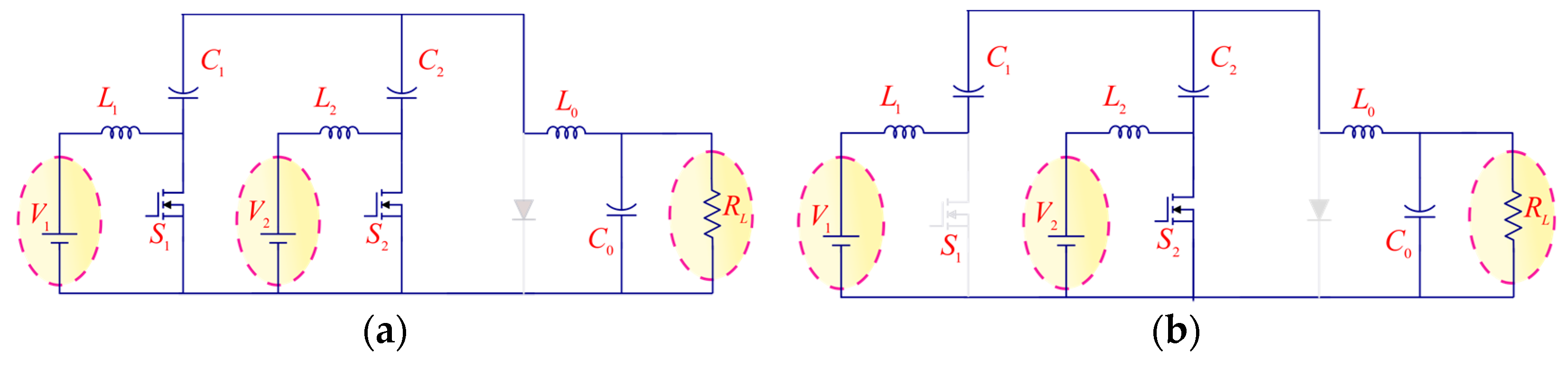
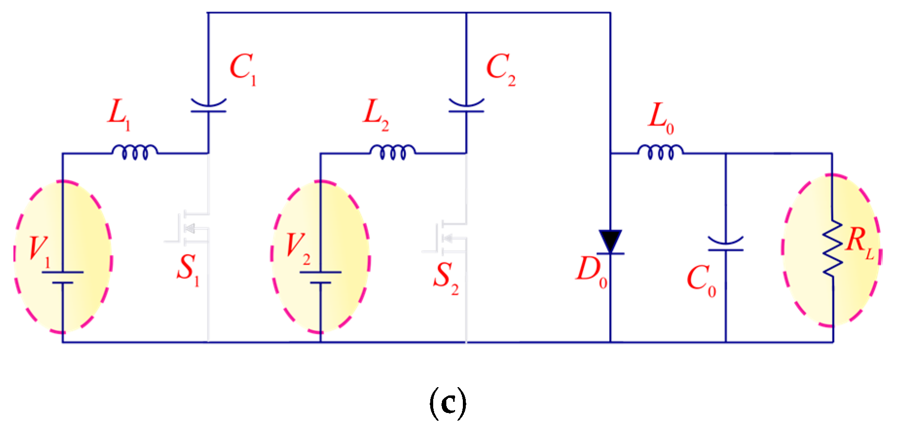
2.2. Operating Principles
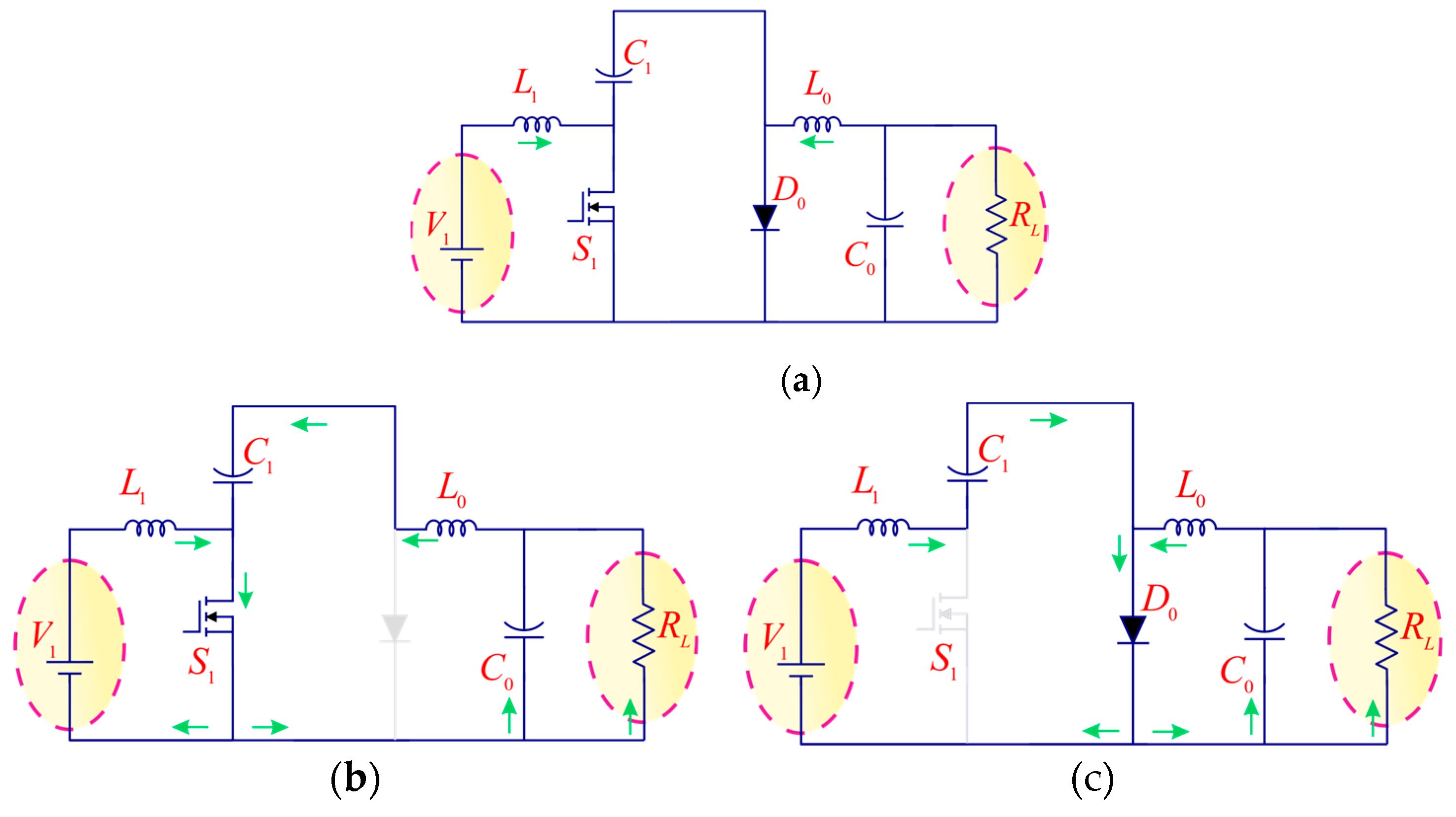
2.2.1. SISO Mode
State 1
State 2
2.2.2. DISO Mode
State 1
State 2
State 3
3. Modeling and Analysis of the Converter
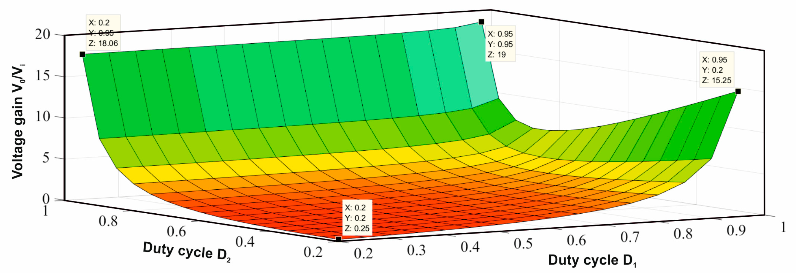
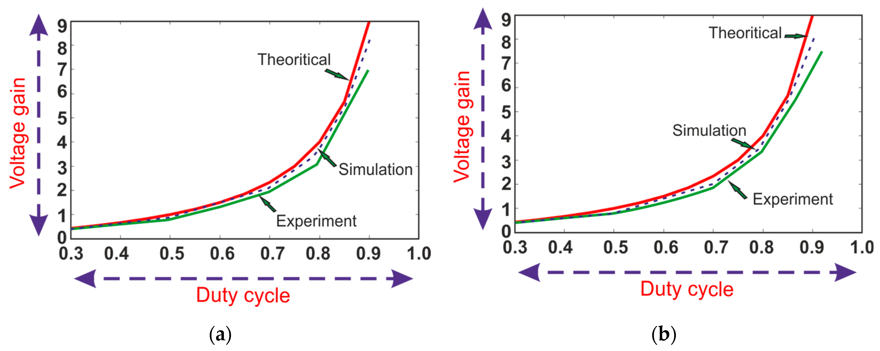
3.1. Voltage Gain
3.2. Current Ripples of Inductors
3.3. Voltage Ripples of Capacitors
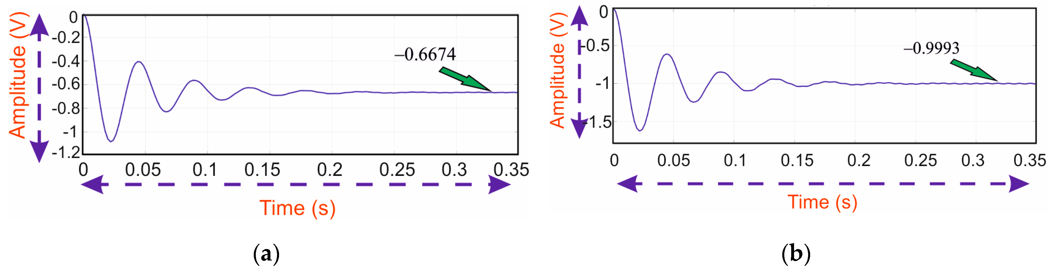
3.4. Small-Signal Modeling
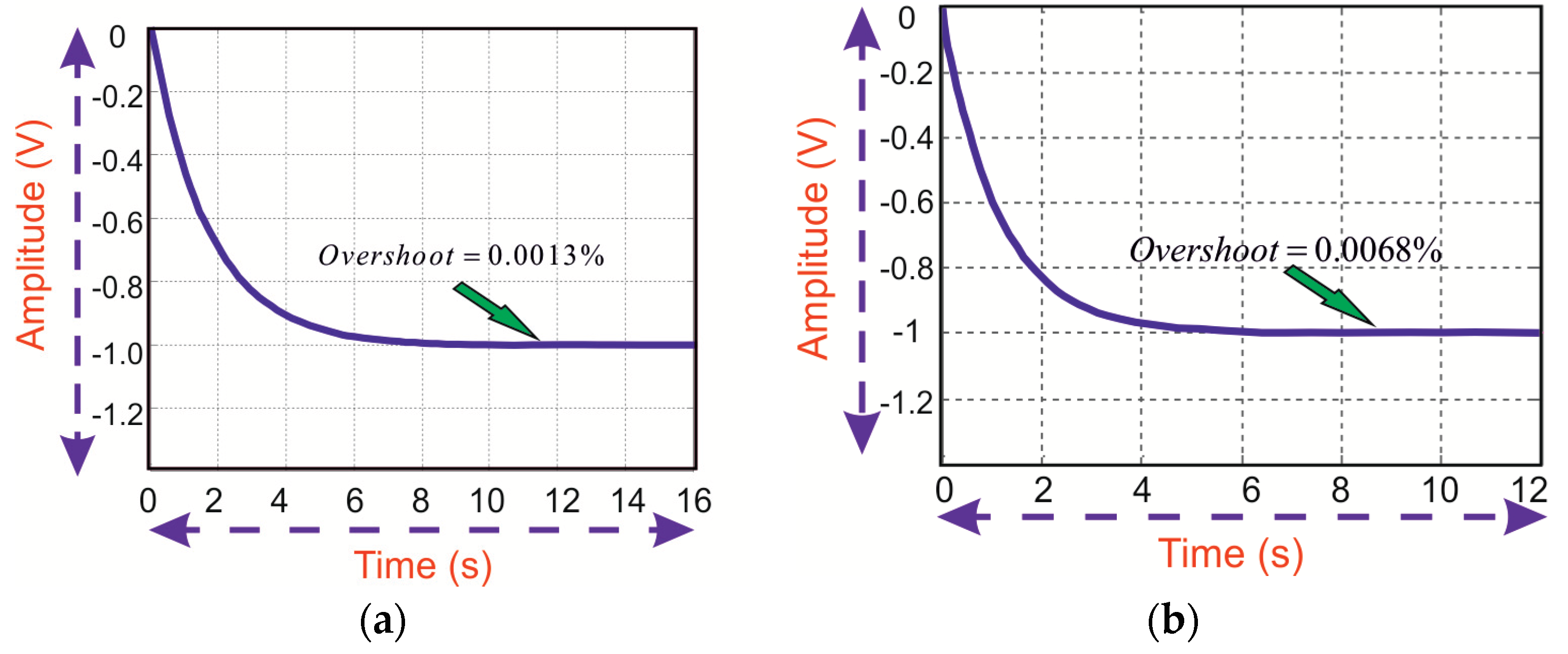
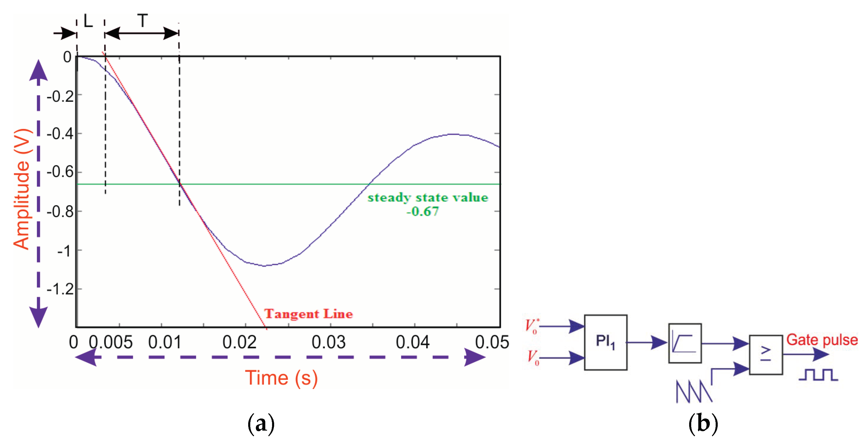
4. Design of Controller
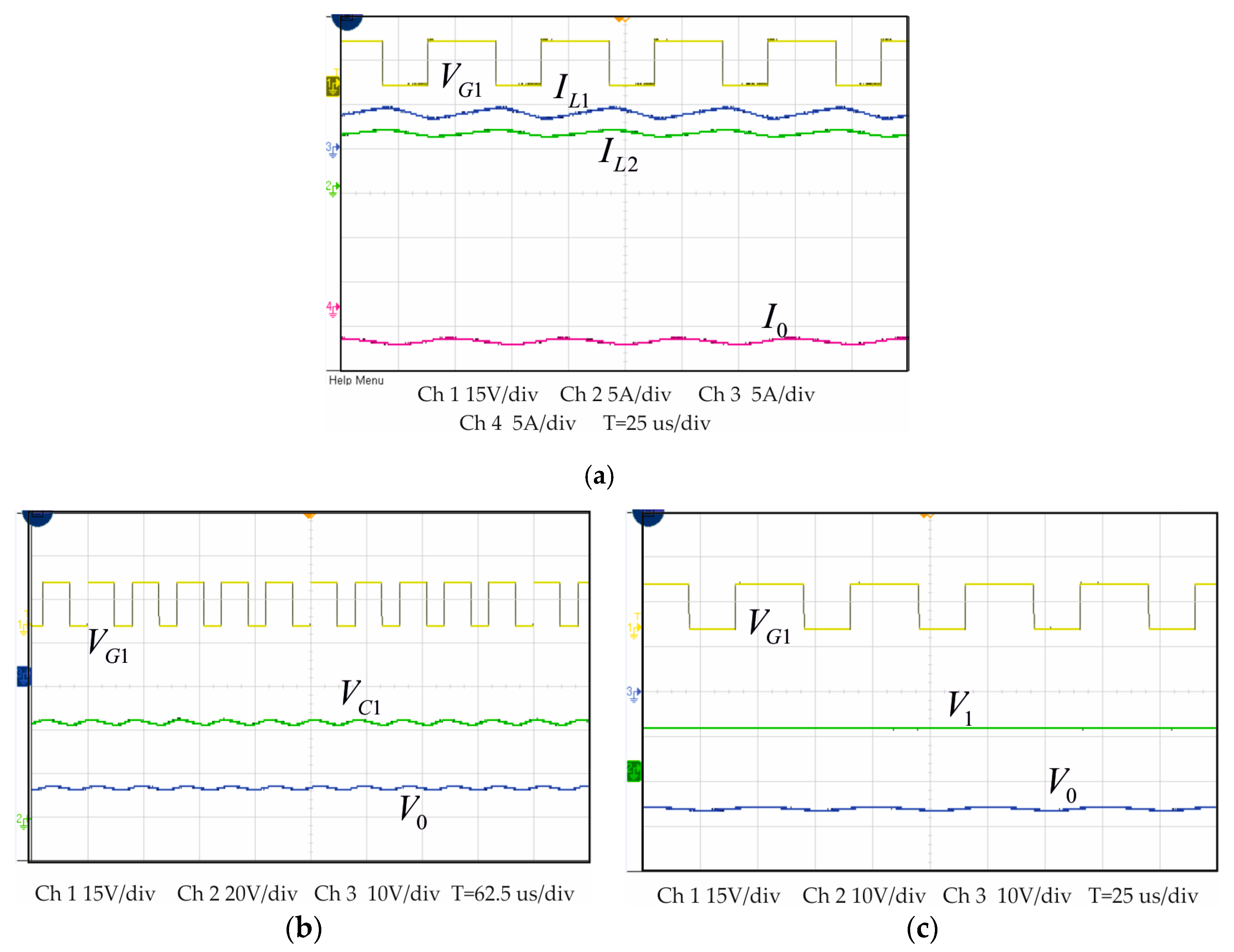
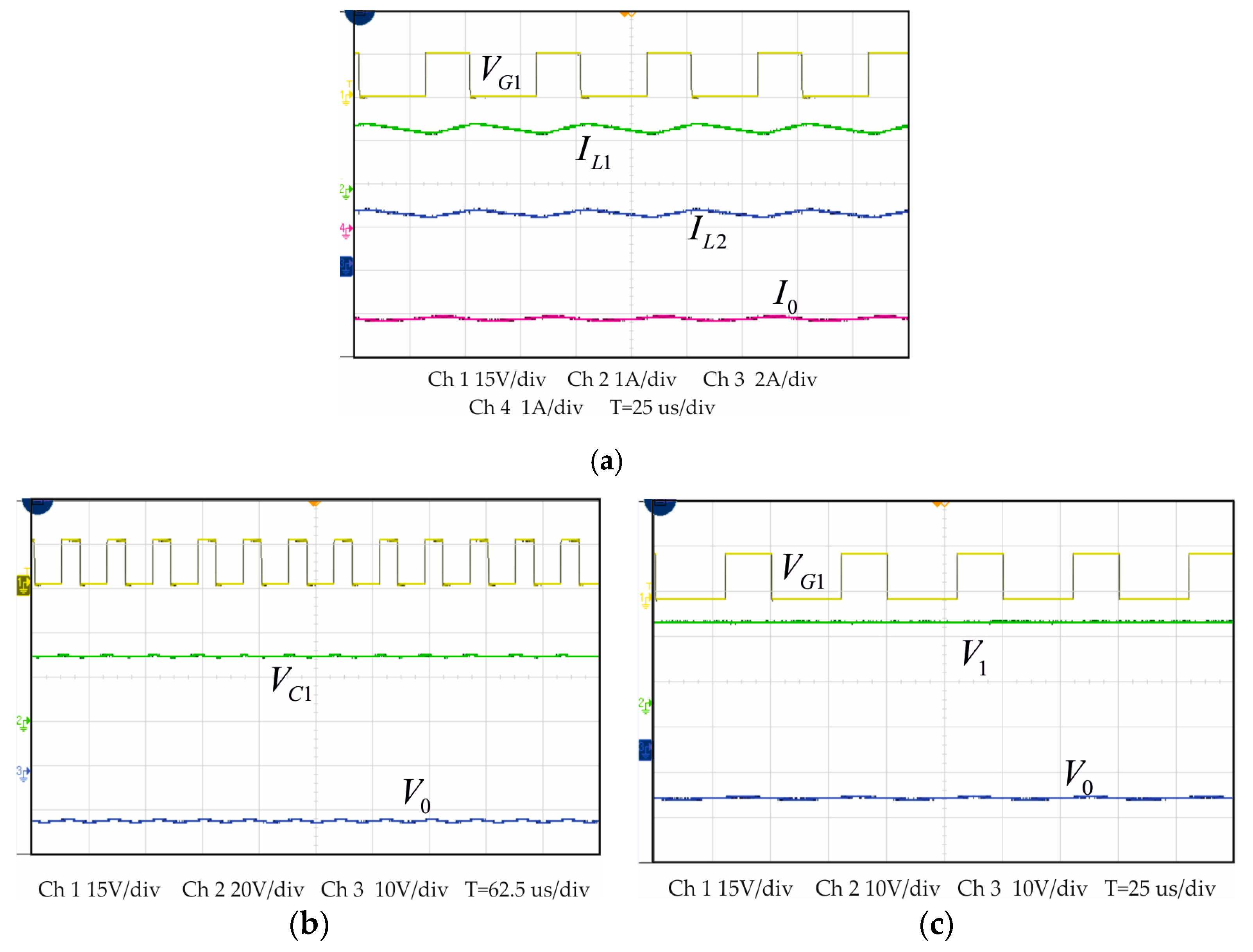
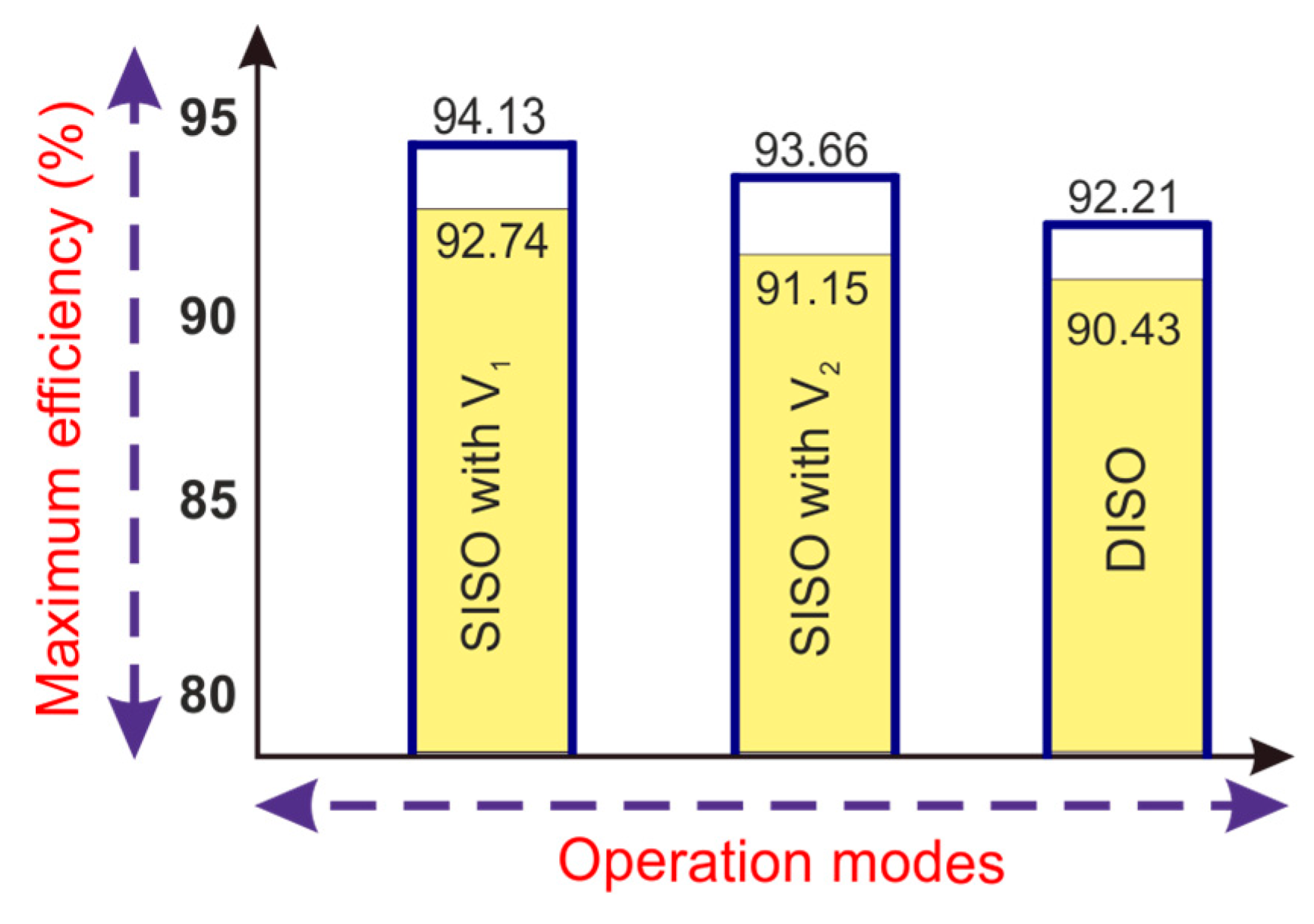
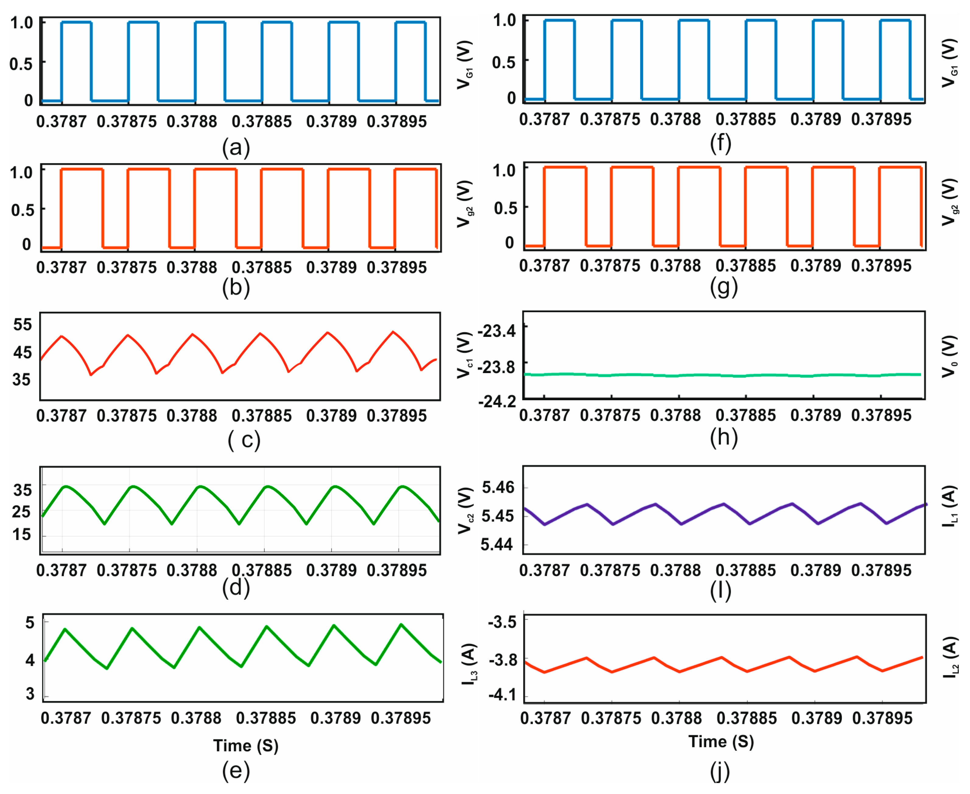
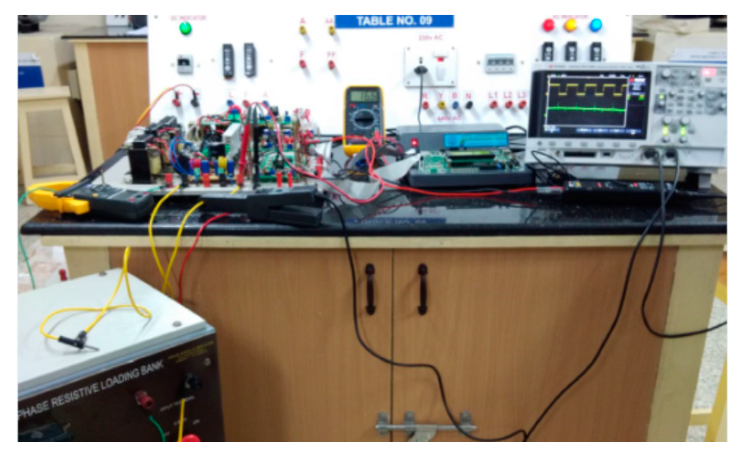
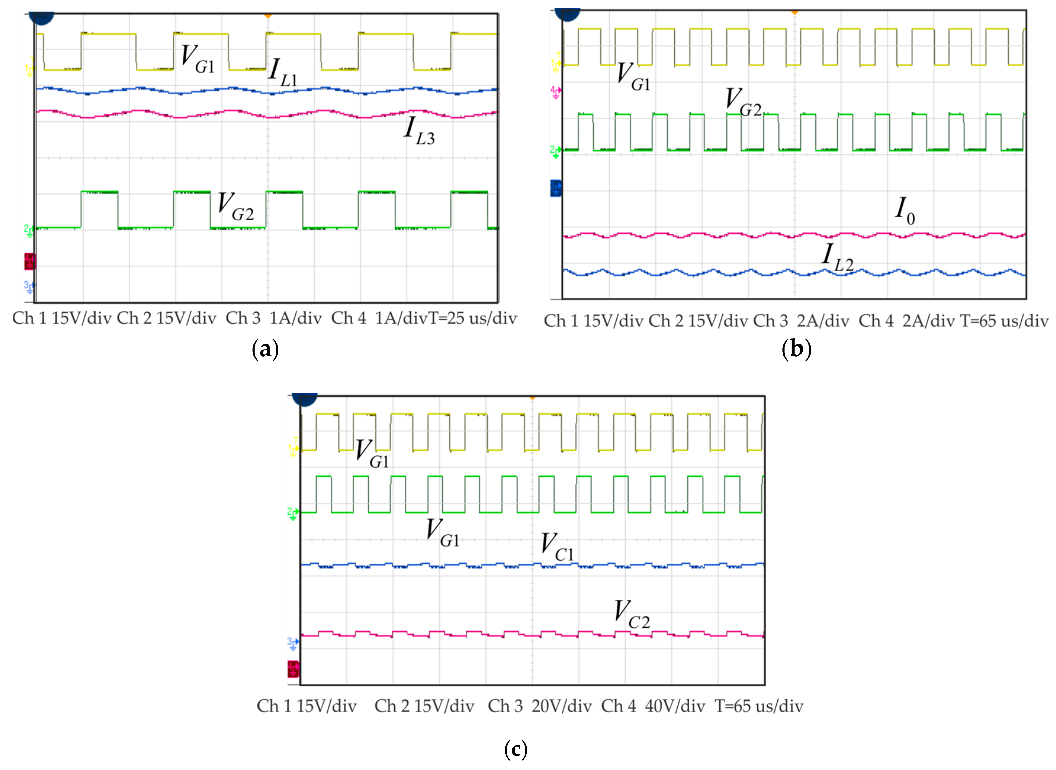
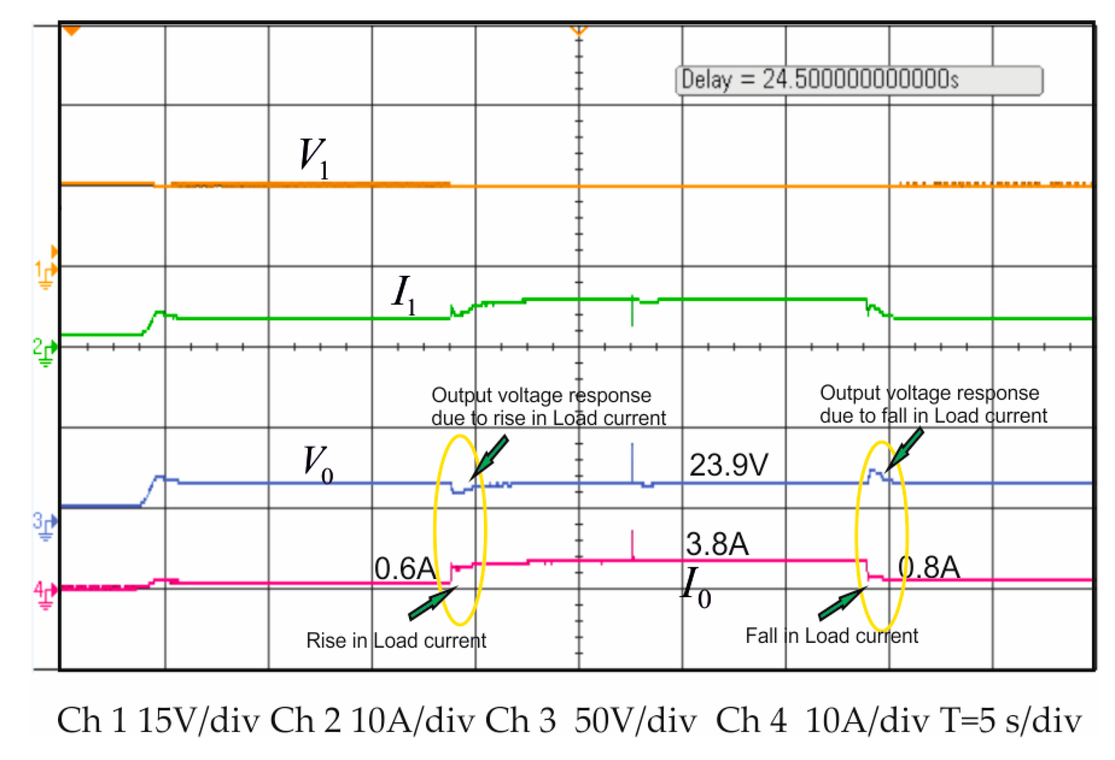
5. Results and Discussion
6. Conclusions
Author Contributions
Funding
Acknowledgments
Conflicts of Interest
References
- Wang, J.; Dunford, W.G.; Mauch, K. Synthesis of two-inductor DC-DC converters. In Proceedings of the Power Electronics Specialists Conference, Saint Louis, MO, USA, 27 June 1997; pp. 1367–1373. [Google Scholar]
- Landsman, E.E. A unifying derivation of switching DC-DC converter topologies. In Proceedings of the IEEE Power Plectronics Ppecialists Ponference, San Diego, CA, USA, 18–22 June 1979; pp. 18–22. [Google Scholar]
- Khaligh, A.; Cao, J.; Lee, Y.-J. A multiple-input DC–DC converter topology. IEEE Trans. Power Electron. 2009, 24, 862–868. [Google Scholar] [CrossRef]
- Kumar, L.; Jain, S. Multiple-input DC/DC converter topology for hybrid energy system. IET Power Electron. 2013, 6, 1483–1501. [Google Scholar] [CrossRef]
- Zhou, Z.; Wu, H.; Ma, X.; Xing, Y. A non-isolated three-port converter for stand-alone renewable power system. In Proceedings of the IECON 2012-38th Annual Conference on IEEE Industrial Electronics Society, Montreal, QC, Canada, 25–28 October 2012; pp. 3352–3357. [Google Scholar]
- Wang, C.-S.; Li, W.; Wang, Y.-F.; Han, F.-Q.; Meng, Z.; Li, G.-D. An isolated three-port bidirectional DC-DC converter with enlarged ZVS region for HESS applications in DC microgrids. Energies 2017, 10, 446. [Google Scholar] [CrossRef]
- Reddi, N.K.; Ramteke, M.R.; Suryawanshi, H.M. Dual-Input Single-Output Isolated Resonant Converter with Zero Voltage Switching. Electronics 2018, 7, 96. [Google Scholar] [CrossRef]
- Wu, Y.-E.; Chiu, P.-N. A High-Efficiency Isolated-Type Three-Port Bidirectional DC/DC Converter for Photovoltaic Systems. Energies 2017, 10, 434. [Google Scholar] [CrossRef]
- De Morais, J.L.S.; Gules, R. Three-port converter based on the bidirectional Ćuk and the LC series-resonant half-bridge topologies for renewable energy applications. In Proceedings of the Industry Applications (INDUSCON), Curitiba, Brazil, 20–23 November 2016; pp. 1–8. [Google Scholar]
- Zhu, H.; Zhang, D.; Zhang, B.; Zhou, Z. A nonisolated three-port dc–dc converter and three-domain control method for PV-battery power systems. IEEE Trans. Ind. Electron. 2015, 62, 4937–4947. [Google Scholar] [CrossRef]
- Georgious, R.; Garcia, J.; Garcia, P.; Navarro-Rodriguez, A. A Comparison of Non-Isolated High-Gain Three-Port Converters for Hybrid Energy Storage Systems. Energies 2018, 11, 658. [Google Scholar] [CrossRef]
- Fong, Y.; Cheng, K.; Raman, S.R.; Wang, X. Multi-Port Zero-Current Switching Switched-Capacitor Converters for Battery Management Applications. Energies 2018, 11, 1934. [Google Scholar] [CrossRef]
- Chen, Y.-M.; Liu, Y.-C.; Wu, F.-Y. Multi-input DC/DC converter based on the multiwinding transformer for renewable energy applications. IEEE Trans. Ind. Electron. 2002, 38, 1096–1104. [Google Scholar]
- Kwasinski, A. Identification of feasible topologies for multiple-input DC–DC converters. IEEE Trans. Ind. Electron. 2009, 24, 856–861. [Google Scholar] [CrossRef]
- Liu, Y.C.; Chen, Y.-M. A systematic approach to synthesizing multi-input DC–DC converters. IEEE Trans. Ind. Electron. 2009, 24, 116–127. [Google Scholar]
- Wu, H.; Xing, Y.; Xia, Y.; Sun, K. A family of non-isolated three-port converters for stand-alone renewable power system. In Proceedings of the IECON 2011-37th Annual Conference on IEEE Industrial Electronics Society, Melbourne, Australia, 7–10 November 2011; pp. 1030–1035. [Google Scholar]
- Wu, H.; Zhang, J.; Xing, Y. A family of multiport buck–boost converters based on DC-link-inductors (DLIs). IEEE Trans. Ind. Electron. 2015, 30, 735–746. [Google Scholar]
- Cheng, T.; Lu, D.D.-C.; Qin, L. Non-Isolated Single-Inductor DC/DC Converter with Fully Reconfigurable Structure for Renewable Energy Applications. IEEE Trans. Circuits Syst. Express Briefs 2018, 65, 351–355. [Google Scholar] [CrossRef]
- Zhao, J.; Iu, H.H.C.; Fernando, T.; An, L.; Lu, D.D.-C. Design of a non-isolated single-switch three-port DC-DC converter for standalone PV-battery power system. In Proceedings of the 2015 IEEE International Symposium on Circuits and Systems (ISCAS), Lisbon, Portugal, 24–27 May 2015; pp. 2493–2496. [Google Scholar]
- Cuk, S. A new zero-ripple switching DC-to-DC converter and integrated magnetics. IEEE Trans. Magn. 1983, 19, 57–75. [Google Scholar] [CrossRef] [Green Version]
- Almalaq, Y.; Matin, M. Three topologies of a non-isolated high gain switched-inductor switched-capacitor step-up cuk converter for renewable energy applications. Electronics 2018, 7, 94. [Google Scholar] [CrossRef]
- Kumar, M.; Babu, Y.N.; Pullaguram, D.; Mishra, S. A high voltage gain non-isolated modified three-port DC/DC converter based on integrated Boost-Cuk topology. In Proceedings of the Asia-Pacific Power and Energy Engineering Conference (APPEEC), Bangalore, India, 8–10 November 2017; pp. 1–6. [Google Scholar]
- Biswas, S.; Dhople, S.; Mohan, N. A three-port bidirectional dc-dc converter with zero-ripple terminal currents for pv/microgrid applications. In Proceedings of the IECON 2013-39th Annual Conference of the IEEE Industrial Electronics Society, Vienna, Austria, 10–13 November 2013; pp. 340–345. [Google Scholar]
- Biswas, S.; Dhople, S.; Mohan, N. Zero-ripple analysis methods for three-port bidirectional integrated magnetic Ćuk converters. In Proceedings of the IECON 2014-40th Annual Conference of the IEEE Industrial Electronics Society, Dallas, TX, USA, 29 October–1 November 2014; pp. 1889–1895. [Google Scholar]
- Ferrera, M.B.; Litran, S.P.; Aranda, E.D.; Marquez, J.M.A. A converter for bipolar DC link based on SEPIC-Cuk combination. IEEE Trans. Power Electron. 2015, 30, 6483–6487. [Google Scholar] [CrossRef]
- Chen, Y.; Zhang, P.; Zou, X.; Kang, Y. Dynamical modeling of the non-isolated single-inductor three-port converter. In Proceedings of the Applied Power Electronics Conference and Exposition (APEC), Fort Worth, TX, USA, 16–20 March 2014; pp. 2067–2073. [Google Scholar]
- Sato, Y.; Nagata, H.; Uno, M. Non-isolated multi-port converter integrating PWM and phase-shift converters. In Proceedings of the Region. 10 Conference, Penang, Malaysia, 5–8 November 2017; pp. 1097–1102. [Google Scholar]
- Yang, H.; Chao, K.; Sun, X.; An, S.; Ren, B.; Zhang, Q. Analysis, modeling and control of a non-isolated four-port dc-dc converter for independent photovoltaic power generation system. In Proceedings of the IECON 2017-43rd Annual Conference of the IEEE Industrial Electronics Society, Beijing, China, 29 October –1 November 2017; pp. 7731–7735. [Google Scholar]
- Balaji, C.; Dash, S.S.; Hari, N.; Babu, P.C. A four port non-isolated multi input single output DC-DC converter fed induction motor. In Proceedings of the 2017 IEEE 6th International Conference on Renewable Energy Research and Applications (ICRERA), San Diego, CA, USA, 5–8 November 2017; pp. 631–637. [Google Scholar]
- Akar, F.; Tavlasoglu, Y.; Ugur, E.; Vural, B.; Aksoy, I. A bidirectional nonisolated multi-input DC–DC converter for hybrid energy storage systems in electric vehicles. IEEE Trans. Veh. Technol. 2016, 65, 7944–7955. [Google Scholar] [CrossRef]
- Chen, Y.-M.; Huang, A.Q.; Yu, X. A high step-up three-port DC–DC converter for stand-alone PV/battery power systems. IEEE Trans. Power Electron. 2013, 28, 5049–5062. [Google Scholar] [CrossRef]


| Circuit Elements | Proposed n-Port Cuk-Cuk Converter | (n-1) Individual Cuk Converters |
|---|---|---|
| Inductors | n | 2(n-1) |
| Capacitors | n | 2(n-1) |
| Switch | n-1 | n |
| Diode | 1 | 2(n-1) |
| Sl.No | Component | Symbol | Simulation | Hardware |
|---|---|---|---|---|
| 1 | Inductors | L1 and L2 | 0.8 & 1.51 mH | 1 & 1.5 mH |
| 2 | Capacitors | C1 and C2 | 46.3 μF & 63 μF | 50 μF, 63 V & 72 μF, 50 V |
| 3 | Output Inductor | L0 | 2 mH | 2 mH |
| 4 | Output Capacitor | C0 | 1.7 μF | 2.2 μF, 35 V |
| 5 | Load Resistance | R | 5.76 Ω | 6 Ω |
| 6 | Switching Frequency | fsw | 20 kHz | 20 kHz |
| Circuit Elements | [5] | [10] | [22] | [30] | [31] | The Proposed Converter |
|---|---|---|---|---|---|---|
| Topology | Nonisolated | Nonisolated | Nonisolated | Nonisolated | Nonisolated | Nonisolated |
| Inductors | 2 | 3 | 2 | 2 | 2 coupled | 3 |
| Capacitors | 3 | 4 | 3 | 1 | 3 | 3 |
| Active switches | 4 | 3 | 3 | 4 | 5 | 2 |
| Diodes | 2 | 1 | 4 | 2 | Nil | 1 |
| Common ground | Yes | Yes | Yes | Yes | Yes | Yes |
| Continuous current at all the ports | No | Yes | No | No | No | Yes |
| Prototype rating | 400 W | 1.2 kW | 200 W | 1 kW | 200 W | 100 W |
| Switching frequency | 100 kHz | 100 kHz | 40 kHz | 20 kHz | 50 kHz | 20 kHz |
| Maximum efficiency | 96% | 93.5% | 92.7% | 95.5% | 90.1% | 94.13% |
© 2019 by the authors. Licensee MDPI, Basel, Switzerland. This article is an open access article distributed under the terms and conditions of the Creative Commons Attribution (CC BY) license (http://creativecommons.org/licenses/by/4.0/).
Share and Cite
Chandrasekar, B.; Nallaperumal, C.; Dash, S.S. A Nonisolated Three-Port DC–DC Converter with Continuous Input and Output Currents Based on Cuk Topology for PV/Fuel Cell Applications. Electronics 2019, 8, 214. https://doi.org/10.3390/electronics8020214
Chandrasekar B, Nallaperumal C, Dash SS. A Nonisolated Three-Port DC–DC Converter with Continuous Input and Output Currents Based on Cuk Topology for PV/Fuel Cell Applications. Electronics. 2019; 8(2):214. https://doi.org/10.3390/electronics8020214
Chicago/Turabian StyleChandrasekar, Balaji, Chellammal Nallaperumal, and Subranshu Sekhar Dash. 2019. "A Nonisolated Three-Port DC–DC Converter with Continuous Input and Output Currents Based on Cuk Topology for PV/Fuel Cell Applications" Electronics 8, no. 2: 214. https://doi.org/10.3390/electronics8020214
APA StyleChandrasekar, B., Nallaperumal, C., & Dash, S. S. (2019). A Nonisolated Three-Port DC–DC Converter with Continuous Input and Output Currents Based on Cuk Topology for PV/Fuel Cell Applications. Electronics, 8(2), 214. https://doi.org/10.3390/electronics8020214