1. Introduction
Millimeter-wave is the frequency portion of the radiofrequency spectrum included between 30 and 300 GHz, i.e., those frequency values for which the wavelength (in air) is between 1 cm and a 1 mm. Millimeter-wave low-noise amplifiers (mmw-LNA) are the key-component in many receiving systems for high-end applications, especially those where system sensitivity is the main parameter.
Systems requiring high-performance receivers are scientific instruments for observation of the universe [
1] or space-borne earth-sensing. Such instruments are based on interferometric techniques synthesized by large arrays or very large parabolic dishes. The receiver relies on specific niche technologies often cryogenically cooled to enhance system sensitivity.
As semiconductor technologies improve their performance, and most of all become more reliable, satellite telecom systems or ground-based safety and security applications (concealed weapon detectors, vehicular guidance, and so on) are becoming more practical [
2]. Finally, wireless communication systems are also moving to millimeter-wave since technologies featuring gate lengths shorter than 100 nm are becoming relatively inexpensive and more easily accessible worldwide.
As a consequence, there is also need for mmw-LNA realized with industrial-grade technology.
2. State-of-the-Art Technologies for mmw-LNA
Low-noise amplification at millimeter-wave requires semiconductor technologies with a current gain cut-off frequency (fT) well above the few hundreds of GHz limit, in order to provide acceptable performance at least up to 300 GHz. Few technologies are capable of fulfilling such requirement and even less are industrial-grade ones. Most are available in research labs, and some, typically the ones originating in the USA, may be subject to export restriction or end user certification.
Current state-of-the-art mmw-LNA are realized either in indium phosphide (InP) high electron mobility transistor (HEMT) or gallium arsenide (GaAs) metamorphic HEMT (mHEMT) with gate lengths shorter than 100 nm. The latter parameter represents, nowadays, a “threshold” value for millimeter-wave operation. In fact, the great majority of mmw-LNAs analyzed in this review are realized featuring a gate length equal or shorter than 100 nm.
HEMT is in hetero-structure transistor where a two-dimensional electron gas (2DEG) is created at the interface of two different contacting material due to their different energy bandgaps. Such 2DEG present very high electron saturation velocity and is well suited for high-frequency and low-noise applications.
In the following, the main features of each technology and how each one can be gainfully employed to achieve low-noise performance are briefly described. Akgiray et al. provide a recent and detailed analysis of technologies for ultra-low-noise applications for operation at millimeter-wave and the relative transistor noise model in [
3].
2.1. Indium Phosphide
InP HEMT transistors have long been the semiconductor of choice for extremely low-noise amplifiers operating in RF, microwave, and millimeter-wave bands due to their superior noise and gain performance up to 300 GHz and even above. Significantly developed in the 1990s, InP HEMT monolithic microwave integrated circuits (MMICs) can be found in both defense applications (such as secure communications) and scientific applications, which typically consist of some form of very high-frequency radiometry, capable of detecting the vanishing small signals travelling from outer space. On the other hand, among all semiconductors, InP experiences slow development due to its niche market and, consequently, tends to be one of the most expensive. Moreover, InP HEMT are unpractical to manufacture, especially in high volumes and, therefore, are relegated to be employed in non-critical applications. Finally, InP technology is extremely well suited for cryogenically cooled operation.
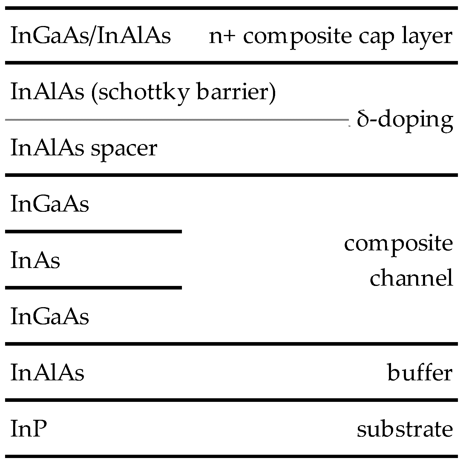
In the case of InP HEMTs, the hetero-structure, schematically depicted in
Figure 1, is formed by In
xGa
1−xAs/In
yAl
1−yAs.
Lattice-matched HEMTs are obtained when x = 0.53 and y = 0.52 while strained structures for x > 0.7. Lattice-matched structures are more easily manufactured but noise performance improves as x → 1. In fact, increasing the channel Indium concentration beyond the 53% lattice-matched condition results in the channel being under compressive strain as the lattice constant of the channel is less than that of the substrate and barrier layers. Providing the channel thickness is kept below some critical value, which depends on the indium concentration, the strain can be accommodated fully in the channel, which takes on the lattice constant of the InP substrate, resulting in a non-lattice-matched device. Increasing the indium concentration results in two effects from modification of the band structure of the channel layer:
The energy separation of the Γ and L valleys increases, meaning that carriers can accelerate for longer in the high mobility Γ valley, and so attain a higher velocity before being scattered into the low mobility L valley.
The electron effective mass reduces, resulting in yet higher carrier mobility in the Γ valley.
Both these effects increase the average velocity of carriers in the device channel and result in an increase in device trans-conductance and
fT for a given gate length. The negative side of increasing the indium concentration is that the bandgap of the channel is reduced. This leads to greater impact ionization that reduces the device breakdown voltage, thus limiting the usefulness of such devices in realistic circuit applications. Consequently, InP breakdown voltage is rather low and typically does not exceed 2.5 V [
3], making this process unpractical in medium-power applications. Examples are of available InP technologies are described in the following paragraphs.
2.1.1. Chalmers University of Technology
The epitaxial structure of this process, schematically depicted in
Figure 1 and reported in greater detail in [
4], consists of a typical lattice-matched structure (
x = 0.53 and
y = 0.52). From top to bottom: A 20 nm In
0.53Ga
0.47As cap layer doped to a Si concentration of 5 × 10
19 cm
−3, an 11 nm In
0.52Al
0.48As barrier, a (5 × 10
12) cm
−2 Si-delta doping, a 3 nm In
0.52Al
0.48As spacer, a 15 nm In
0.65Ga
0.35As channel, and a 250 nm In
0.52Al
0.48As buffer.
Hall measurements at room temperature of the structure with the cap layer etched away demonstrated electron mobility and sheet carrier concentration of 11,400 cm2/V⋅s and 2.8 × 1012 cm−2, respectively. The source–drain distance is 1.2 μm, while the gate length is 130 nm.
2.1.2. NGC, Northrop Grumman Corporation
Northrop Grumman Corporation’s (NGC) 35 nm InP HEMT process [
5] has produced state-of-the-art results well above 100 GHz, as reported in
Section 4. Two variants of the process are available with different indium mole fractions in the active In
xGa
1-xAs layer,
x = 0.75 and
x = 1.0, respectively. Both processes are grown on a 50-μm-thick substrate in order to guarantee adequate performance at extremely high frequencies. The version with 100% Indium content has approximately 35% higher trans-conductance (
gm) than the version with 75% Indium: 2300 vs. 1700 mS/mm.
2.1.3. ETH Zürich
ETH Zürich developed a very interesting 100 nm InP pHEMT process [
6,
7]. Starting from the 4 inch semi-insulating InP substrate, the layer stack consists of an InAlAs buffer, a pseudomorphic In
0.68Ga
0.32As channel, an In
0.45Al
0.55As Spacer, a Si delta-doped layer, an In
0.45Al
0.55As barrier, a 3 nm InP etch stop layer, and an n
+ InGaAs cap layer. Hall measurements conducted at room temperature show an electron mobility of 12,000 cm
2/V
·s and a sheet carrier density of 3.0 × 10
12 cm
−2. This technology shows a
fT and
fMAX up to 270 GHz and 350 GHz, respectively, and a maximum
gm equal to 1100 mS/mm, thus enabling advanced performance with very low power consumption. The average minimum noise figure associated with this technology in the DC–20 GHz frequency band is 0.3 dB, with an associated gain equal to 18.3 dB at 10 GHz.
2.2. Gallium Arsenide
The advantages of GaAs substrate over InP are lower manufacturing costs, improved power handling capability, and larger wafer size available for production [
8]. Due to increasing number of receiving elements, there is an emphasis on cost, yield, and process stability. Consequently, GaAs is commercially more attractive and has enjoyed significant investment in process development over the last decade.
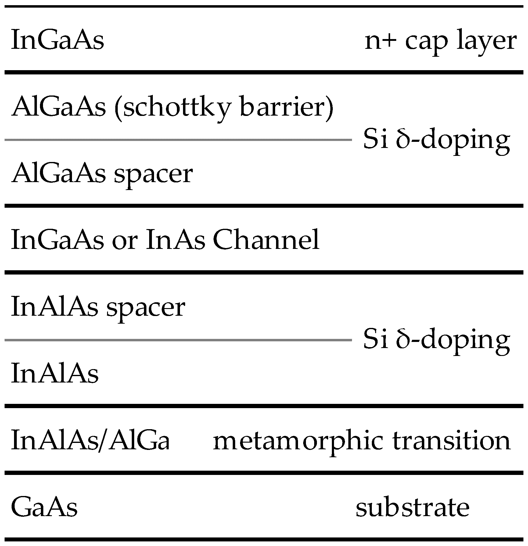
Good crystal quality is achieved with the use of a metamorphic transitional buffer layers between the GaAs substrate and the active device layers of the InGaAs/InAlAs family to adapt the Indium lattice constant in the active channel to the GaAs substrate. A typical epitaxial hetero-structure of GaAs mHEMT is shown in
Figure 2.
2.2.1. IAF, Fraunhofer Institute for Applied Solid State Physics
The technology is based on a 50 nm or 35 nm gate-length InAlAs/InGaAs mHEMT [
9]. A metamorphic buffer is used for a lattice-matched growth of the HEMT layers on 100 μm semi-insulating GaAs wafers. The 2DEG is confined in a composite In
0.8Ga
0.2As/In
0.53Ga
0.47As channel. After the front side process, a full back side process follows. This includes wafer thinning to 50 µm thickness, through substrate via holes, and back side metallization. Apart from the standard process, a noise-optimized variation is available. The major difference is that the “noise-variant” utilizes only the In
0.8Ga
0.2As main channel and no composite channel
2.2.2. OMMIC
Transistors are built in a mHEMT technology process, called D007IH, with 70 nm gate length. For such small gate lengths, the static fringing capacitance of the gate becomes the main limitation to performance for the given epitaxial structure. This has led the foundry to develop a double T-shape gate topology (also taking care of the vertical dimension) [
1]. The active component is based on an InGaAs/InAlAs hetero-structure and a conductive channel with 52% and 70% indium content, respectively, to obtain low-noise performance at operating frequencies above 100 GHz. In this process, a special type of graded buffer (metamorphic) is used to ensure an adequate transition between the GaAs substrate and the active layer, which are not lattice matched due to the high indium content. The process provides a current gain cut-off frequency (
fT) of 300 GHz and a maximum oscillation frequency (
fMAX) of 350 GHz [
10]. The drawback for the above-mentioned advanced figures of merits is a rather low breakdown voltage (−3 V), due to the high indium content in the channel. The wafer is typically thinned down to 100 µm or even down to 70 µm when higher frequency operation is required.
2.2.3. BAE Systems Microelectronics Centre
The epitaxial structures for mHEMT fabrication are grown by molecular beam epitaxy on semi-insulating GaAs substrates. The structures consist of a graded InAlAs metamorphic buffer, a high-indium InGaAs channel, an InAlAs gate layer, and a highly doped InGaAs cap layer. Two channel designs are available: Structure A has an 80% InGaAs channel with a silicon planar doping only above the channel, and structure B has a composite channel containing an InAs layer, with silicon planar doping both above and below the channel. For structures A and B, the typical room-temperature sheet carrier densities were around 3.3 × 10
12 and 3.8 × 10
12 cm
−2, respectively. Correspondingly, the room-temperature electron mobility was around 11,500 and 12,000 cm
2/V⋅s. It is worth noting that structure B has both higher sheet carrier density and electron mobility than structure A. On both structures A and B, the gate length is 50 nm [
11].
2.3. HEMT Technology Performance Summary
Table 1 presents a summary of the key features of the listed technologies. All are suitable for very high-frequency applications in conjunction with low power consumption, thanks to high
gm.
3. Design Challenges and Solutions
Designing an mmw-LNA consists of substantiating a viable solution considering the variety of requirements to be tackled.
Technology is the first issue to be investigated, and some indications have already been provided in the previous
Section 2. A very basic (oversimplifying) guideline could be to select InP for the systems where noise figure is the key requirement and reliability–repeatability–cost is not a great concern. Consequently, InP is suitable for radio astronomy and, more generally, all those scientific instruments requiring very high sensitivity. Conversely, GaAs should be employed in those applications were reliability–repeatability–cost is a major system requirement together with the ability of processing medium power signals.
Considering a bottom-up approach, the topics to address are device (bias point and feedback), propagation medium, and finally circuit topology. This design flow is adopted when—for some reason—there is a predefined constraint on the adopted technology, device geometry, and so on. The goal of this approach is to obtain the “best possible” LNA in the framework of the given constraints. On the other hand, a “top-down” approach starts from the analysis of chip-level requirements (noise figure, gain, DC power consumption, port matching, etc.). The designer consequently determines technology, topology, and device in order to fulfil the chip-level requirements. It is worthwhile noting that both procedures are circular rather than straightforward. In other words, some design choice performed in a later stage may affect a previous step, causing one to go back and adjust a parameter decided previously.
Anyhow, the necessary design steps are similar in both cases and only the order in which they are investigated is changed. In the following, a deeper insight of all related aspects for designing mmw-LNA is provided.
3.1. Active Device: Geometry, Bias Point, and Feedback
Accurate device modelling is crucial to increase the chance of obtain a first attempt pass design. Usually devices are characterized linearly up to 100 GHz and for noise at 50 GHz. The model is extrapolated above this frequency and some deviations from real behavior must be accounted for. Another issue concerns de-embedding procedure. The device is probed through a coplanar interface (balanced signal) while the model is provided with an accessible source terminal. Standard de-embedding procedures can be profitable applied up to 50 GHz, but above this frequency, some additional uncertainties occur. Unfortunately, these aspects are outside the designer’s reach, and he must rely on the models supplied by the technology provider.
3.1.1. Device Geometry
The selection of an appropriate gate width for a transistor is an essential part of a low-noise amplifier design flow. This is performed by first selecting an optimum unit gate width for a single finger and then placing these fingers in parallel to form a transistor. Apart from differences because of distributed effects of inter-connects, altering the number of fingers does not affect the gain or minimum noise of the transistor. Therefore, changing the number of fingers can be used to select appropriate device impedances for matching and the output power capability of the transistor. At millimeter-wave, an optimum total periphery (number of fingers multiplied by unit gate width) for low-noise performance in a common-source topology is around 50−100 μm. The number of fingers is typically 2 or 4. A higher number of fingers would involve higher parasitic reactance, making the device impractical for use above 50 GHz.
3.1.2. Optimum Bias Point
Transistor performance, and in particular its gain vs. NF trade-off, greatly depends on the bias point. In fact,
Fmin is directly proportional to the drain current Id through Pospieszalski’s equation:
In Equation (1), f is the frequency of operation, fT is the transistor cut-off frequency at the selected bias point, Rt is the gate resistance, Tg is the ambient temperature, Gds is the transistor output conductance, and Td the transistor channel temperature. Keeping in mind that the channel temperature Td is proportional to the drain current Id in the HEMT. High-frequency operation is obtained when the device’s current gain cut-off frequency (fT) is high (>500 GHz). fT is equal to gm/2Cgs, where gm is the trans-conductance and Cgs the gate-source capacitance. Consequently, HEMTs with a high trans-conductance at a low bias current are preferred to achieve low-noise performance.
In low-noise applications the transistor is biased at a low-noise/medium-gain operating point, which typically corresponds to 15%−20% of I
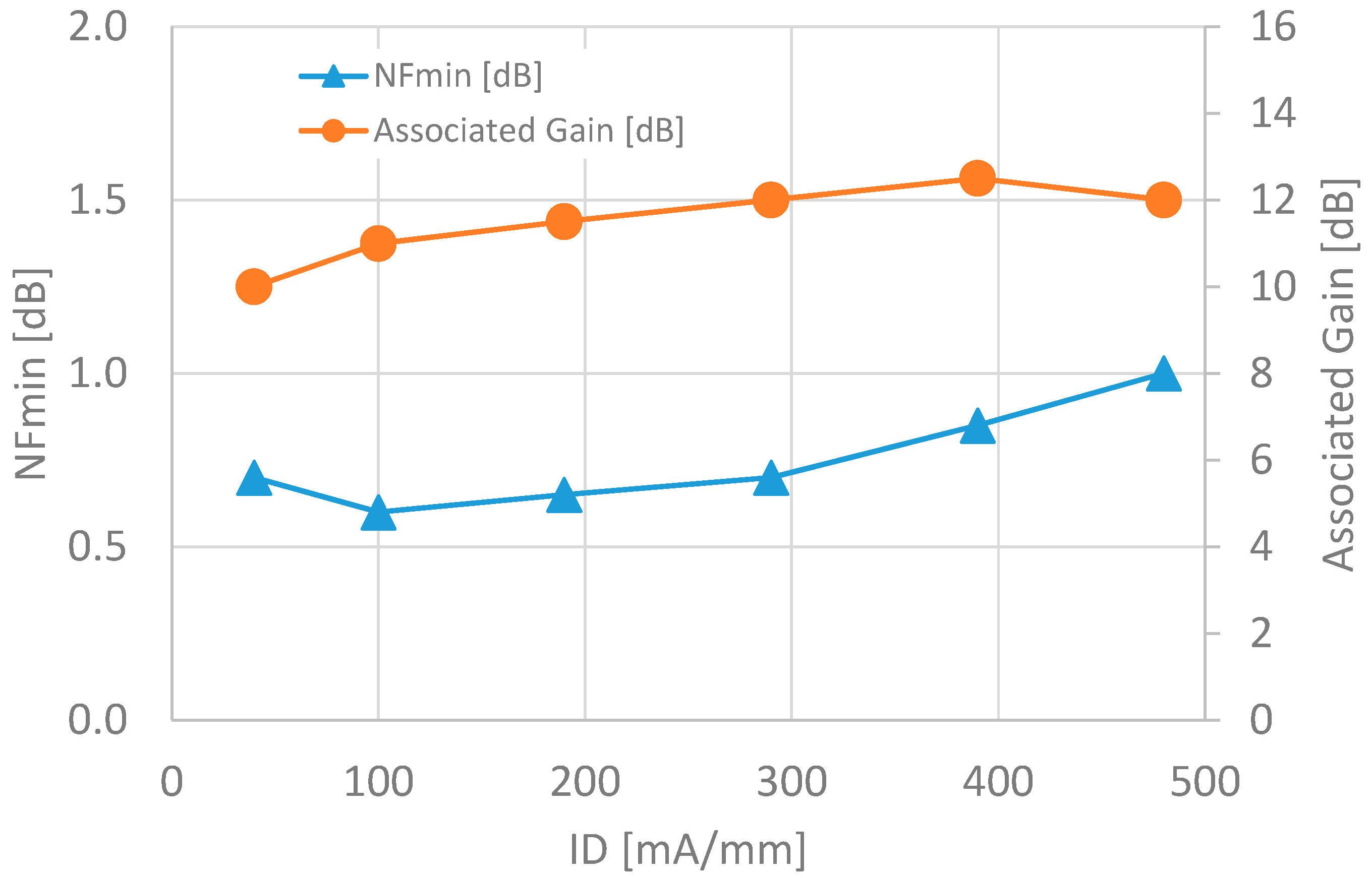
DSS, that is the transistor maximum current. As an example,
Figure 3 reports the minimum noise figure (NF
min) and associated gain at 30 GHz as a function of drain current density I
D (mA/mm) of a two finger 50 μm gate width GaAs mHEMT biased at V
DS = 1.0 V in OMMIC’s D007IH technology. As stated before, there is an optimum bias for noise (at 20% of I
DSS) and optimum bias for gain (at 80% of I
DSS).
3.1.3. Source Degenerative Feedback
This technique, applicable to the common source configuration, consists of inserting an inductive dipole between the FET’s source terminal and ground. This technique is applied for a variety reasons, as follows. First, it lowers the gain of the transistor allowing a wider bandwidth operation. Second, it enables simultaneous signal and noise matching (SSNM) [
12], which is very important since, in general for low-noise devices, the optimum impedances for matching and noise are far from each other. This point also enables a wider bandwidth operation. Third, the gain reduction improves the transistor’s stability, at least in the operating bandwidth.
At lower microwave frequencies, the inductive dipole is realized through a spiral inductor. As the frequency increases, a short and thin microstrip line replaces the spiral inductor. At very high frequencies, the parasitic inductance of the via-hole to ground through the substrate is often enough to obtain the desired effect. In multi-stage amplifiers, as occurs in mmw-LNAs, there are design guidelines that aid the designer in selecting the inductance value for each stage given a gain/stability constraint, with the aim to obtain an input and output match as close as possible to 50 Ω [
13].
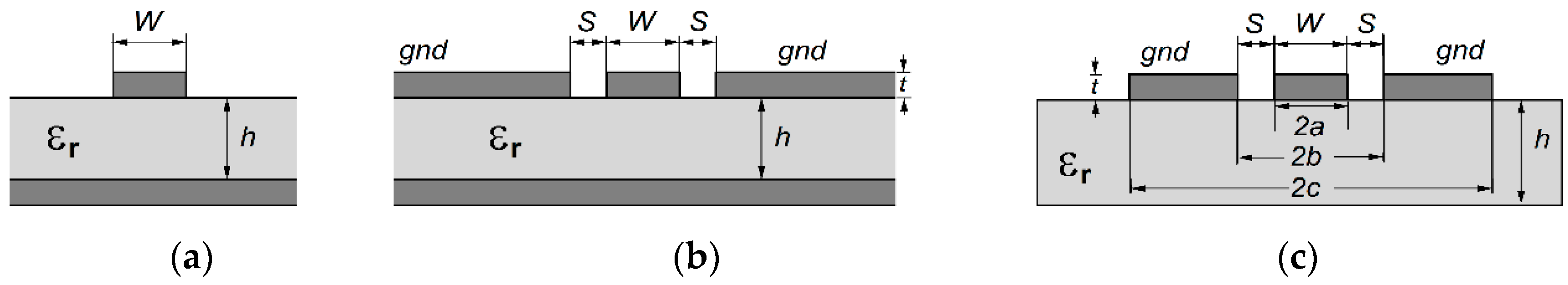
3.2. Propagation at Millimeter-Wave on-Chip
Microstrip has an elegant simplicity to it, which makes it easier to fabricate and even easier to model via computer than coplanar waveguide or its grounded counterpart. With their strong ground structure, coplanar waveguide circuits are capable of lower-loss performance at much higher frequencies than microstrip MMICs and offer great potential for designs working well into the millimeter-wave frequency range. On the other hand, microstrip is probably the most popular transmission-line format but suffers increased circuit losses into the millimeter-wave frequency range, making the circuit technology less efficient for use at frequencies above 100 GHz.
Figure 4 reports commonly used structures for transmission lines at millimeter-wave where also noteworthy geometrical parameters are reported that determine the electrical features of the transmission line, namely characteristic impedance
Z0,C and phase constant
β.
3.2.1. Microstrip
Microstrip, as shown in
Figure 4a, is the most common configuration in MMIC technology, mainly due to the large availability of electrical models (both active and passive), and it also represents the baseline solution in CAD simulation tools. This choice is reasonable up to W-band (110 GHz), after which a series of critical aspects occur that make this configuration unfeasible. As stated in
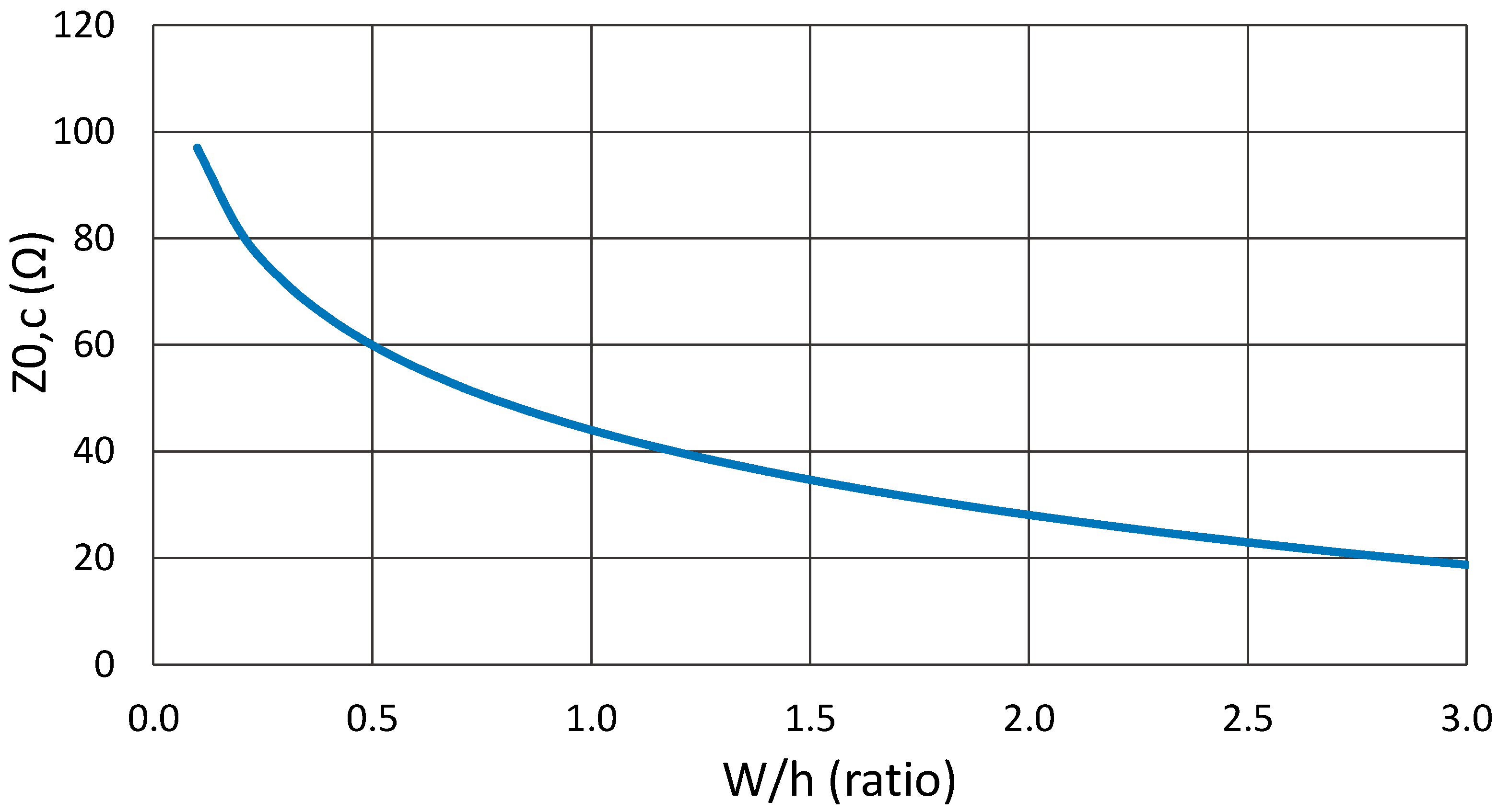
Section 3.1.3, the parasitic inductance of the via-hole to ground through the substrate may become significant, leading to an unacceptable decrease in the gain of the device. A possible solution to this weakness consists of thinning down the wafer to 50 or even 20 μm. Although the inductive effect reduced, the wafer becomes difficult to handle due to the reduced thickness. In any case, resonant modes across the substrate and high-order modes appear when the wavelength of the signal becomes comparable to substrate thickness, and ultimately limit the usable frequency range of the microstrip structure. The dielectric constants of InP and GaAs are quite similar: Respectively, 12.4 and 12.9. The W/h ratio for 50 Ω characteristic impedance in both cases is about 75%. Therefore, a 50 Ω microstrip line will have a width of about 75 μm on a 100 μm thick GaAs or InP substrate. A simplified relation between characteristic impedance the a microstrip transmission line and its W/h ratio is shown in
Figure 4a, and frequencies are provided in Equation (2). This relation is applicable to GaAs and InP substrates at millimeter-wave and is valid for 0.1 < W/h < 3.
Figure 5 contains the plot of the relationship expressed in Equation (2).
3.2.2. Coplanar Waveguide (Grounded or Not)
Coplanar waveguide (CPW) configuration in
Figure 4b,c is particularly helpful in order to circumvent the criticalities sketched in the previous section. The presence of cold conductors on the same plane of the signal line introduces much less losses and couplings through the substrate, allowing the use at higher frequencies. In fact, the parasitic inductance to ground for shunt elements is much lower for CPW, compared to microstrip applications. This is because the RF ground is very close to the transmission line, and there is no need to drill a via-hole through the substrate for ground connection. This, in turn, eases manufacturing issues. However, this solution is all but effortless: The two lateral ground planes make the realization of circuits based on this transmitting structure much more complex, both for the higher bigger overall dimensions and for the need to impose them the same voltage at every section. Furthermore, CAD tools are less oriented towards this configuration and reliable electrical models are often lacking. The same consideration holds for active device models provided by the foundry.
Ground plane is mandatory when the MMIC is going to be mounted in a metallic carrier, which is often the case at millimeter-wave, and the second ground plane is placed on the opposite side of the dielectric. This variant of coplanar waveguide is known as grounded coplanar waveguide (GCPW) and is schematically depicted in
Figure 4b. For a given line impedance, there is, in theory, an infinite number of solutions for the geometry of a GCPW line. In fact, while H appearing in Equation (2) is fixed by the technology provider, in CPGW, the impedance is synthesized by appropriately determining the ratio of W/S, since both width (W) and spacing (S) are a free design variable. The only limit is feasible values for S above a minimum value specified by the foundry rules.
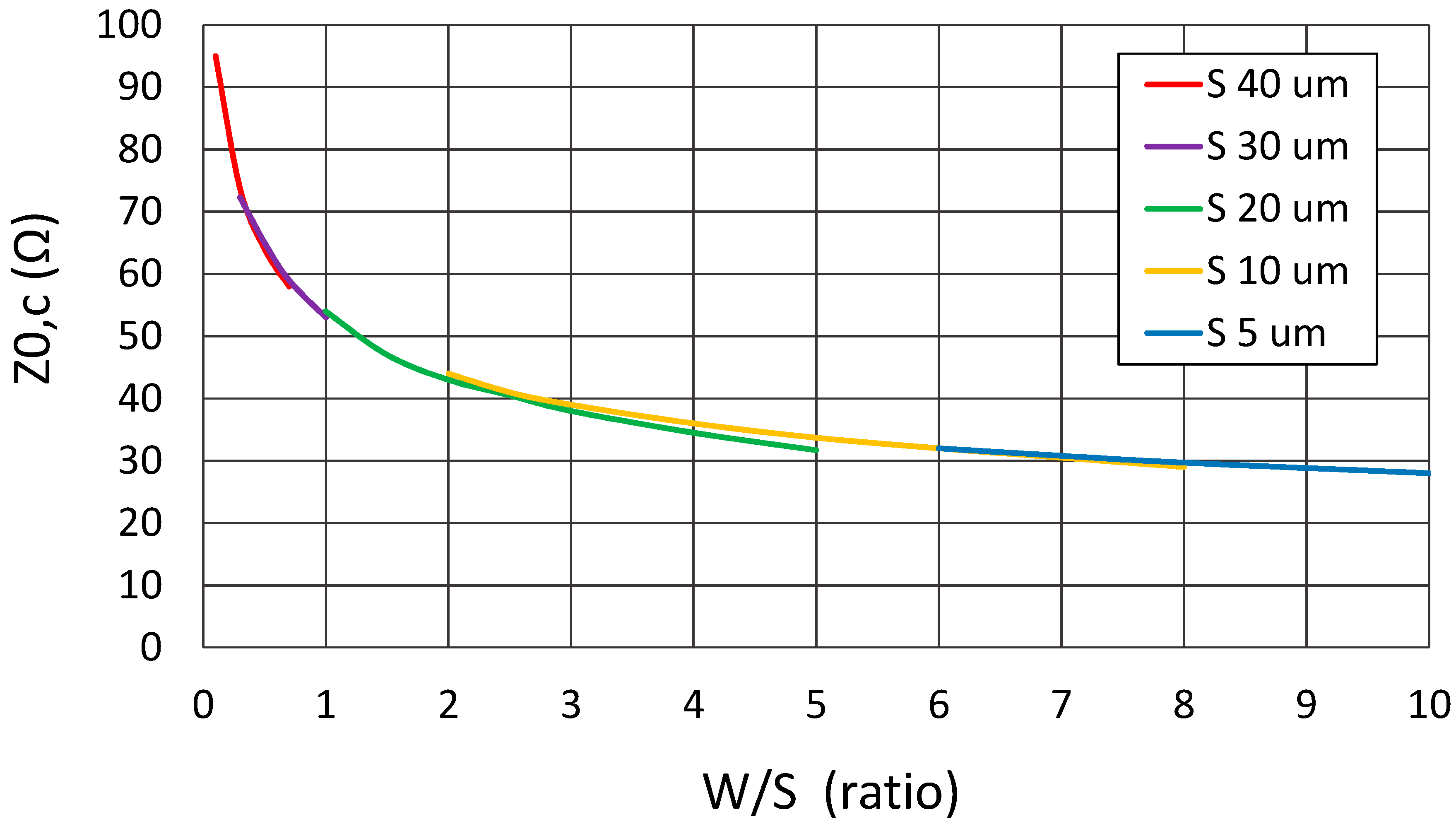
A simplified relation between characteristic impedance of the GCPW transmission line and its W/S ratio, valid at millimeter-wave frequencies, is provided in Equation (3).
This relation is applicable to GaAs and InP substrates and is valid for 0.1 < W/S < 10 and 5 μm < S < 40 μm. In order to obtain feasible values of W, larger values of S are used to synthesize higher characteristic impedance while smaller values of S to obtain lower characteristic impedance.
Figure 6 contains the plot of the relationship expressed in Equation (3). In this case, the curves are parametrized for several values of S in the range from 5 μm to 40 μm. The curves are validated for substrate thickness (h) between 50 and 100 μm.
3.3. Circuit Topologies
Circuit topology is selected to fulfil some system architectural constraint or chip-level requirement. The trade-off to be performed is between circuit complexity and mmw-LNA performance. As the requirements between more stringent, for example ultra-wide operating bandwidth and adequate (>10 dB) input/output return loss, then circuit complexity increases. Fortunately, very low noise figure can be fulfilled even with the simplest circuit topology, as expressed in the following sections.
3.3.1. Single Ended
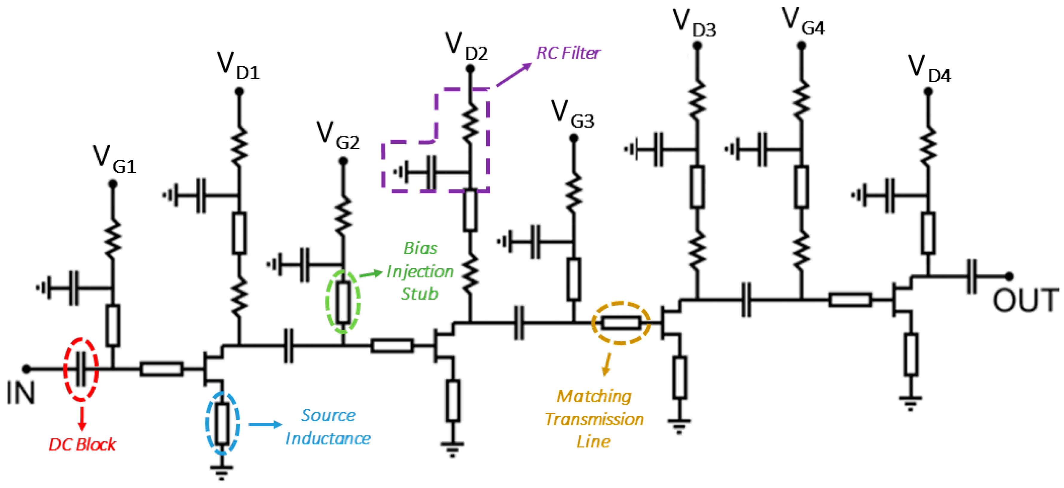
Single ended is by far the most employed topology in mmw-LNA since it is relatively easy to synthesize. At high-operating frequency, a sensible design strategy consists of keeping circuit complexity at the lowest possible level. Single-ended topology consists of cascading a certain number of common source (CS) amplifying stages to obtain the prescribed gain value, obviously within the limitation of a feasible number of stages. A simplified schematic of an N-stage (N = 4) single-ended amplifier is shown in
Figure 7.
Once the active device has been selected, biased cured by feedback, as described in
Section 3.1, the following step consists of determining the number of necessary stages. These usually vary from 3 to 5 as a function of the operating frequency and technology performance. Usually, three stages are sufficient to reach an adequate gain level (>20 dB) at lower millimeter-wave frequencies (i.e., <70 GHz) [
14]. When the frequency increases, then it is not uncommon to find mmw-LNA with more than four stages [
15].
The final step of the design consists of appropriately sizing the components that appear in
Figure 7. Series and shunt transmission lines are used for noise/signal matching (at RF) and transistor biasing (at DC). Series DC-block capacitors are inserted also for matching purposes and their value rarely exceeds 0.3 pF, often even less as the frequency increases. Design practice and analysis of open literature lead to the conclusion that external DC blocking capacitors—i.e., the ones at the LNA’s I/O ports—are larger than the capacitors inserted for inter-stage matching and DC blocking embedded in the LNA. The latter are often half the size or even less of the external capacitors. This is because I/O capacitors are directly linked to the LNA’s I/O matching, while the internal capacitor’s value is chosen to fulfil some gain over frequency requirement and effects the LNA’s I/O match less. External capacitors are in the range of 0.1 to 0.3 pF, while the internal ones can be less than 0.1 pF. Electro-magnetic simulations become mandatory at this point since the capacitance of the internal DC-blocks is comparable to other parasitic capacitance inside the circuit. Finally, resistors and capacitors are used to filter out unwanted signals that may be present in the bias supplies and moreover provide the ohmic losses to stabilize the device at lower frequencies. Please note that in the last stages, resistors are also inserted close to the active device. This technique improves device stability at lower frequencies at the expense of higher stage NF. This is acceptable when the gain of the preceding stages in enough to conceal the higher noise contribution coming from the stages containing the resistors.
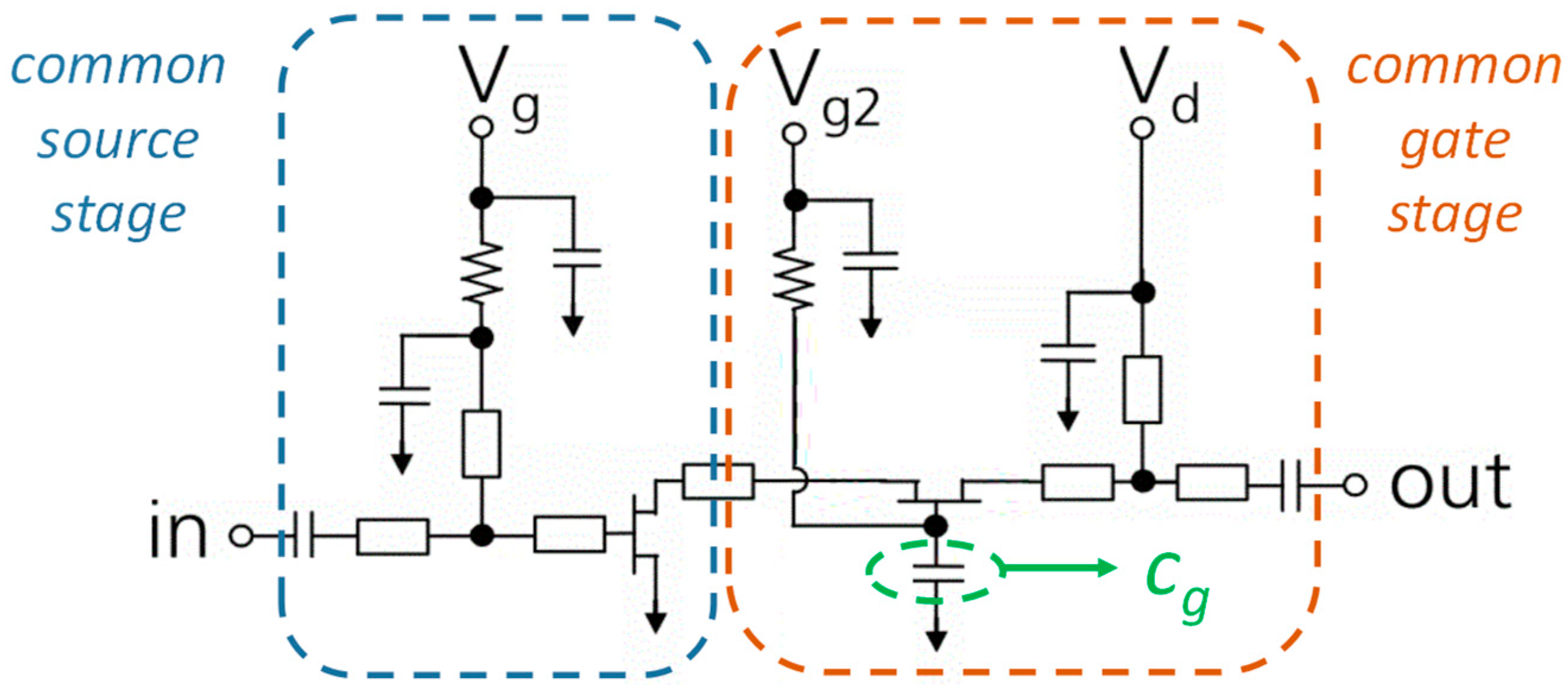
3.3.2. Cascode
Cascode topology represents an interesting solution when large operating bandwidth is a design goal in conjunction with low NF and high gain. In this topology, a common source stage is cascaded with a common gate stage that acts as a wideband low-input impedance buffer stage for the preceding stage. A simplified schematic of a cascode cell is depicted in
Figure 8.
Unfortunately, circuit complexity, with respect to single-ended topology, is somewhat increased for the following reasons. First, the DC drain voltage, Vd in
Figure 8, is divided across the two transistors and, moreover, the current flow in the two transistors is the same by design. Consequently, a detailed DC analysis needs to be carried out. Second, the gate terminal (Vg2) of the common gate stage cannot be DC-grounded but needs to be biased at slightly less half the value of Vd. Consequently, the gate is AC grounded—trough capacitor Cg—and this poses some limitations on the practical operating bandwidth. The technique involves choosing a small and appropriate Cg value to present an optimum load to the drain of the common source transistor of the cascode. This method departs from the conventional practice of choosing a large Cg to provide good AC grounding to the common gate transistor. Typical values of Cg at millimeter-wavelength is around 0.1 pF. Occasionally, a parallel–parallel feedback synthesized through a series R-C connecting the transistor’s drain and gate terminals is applied to the common gate transistor to improve its stability and obtain an even greater bandwidth of operation.
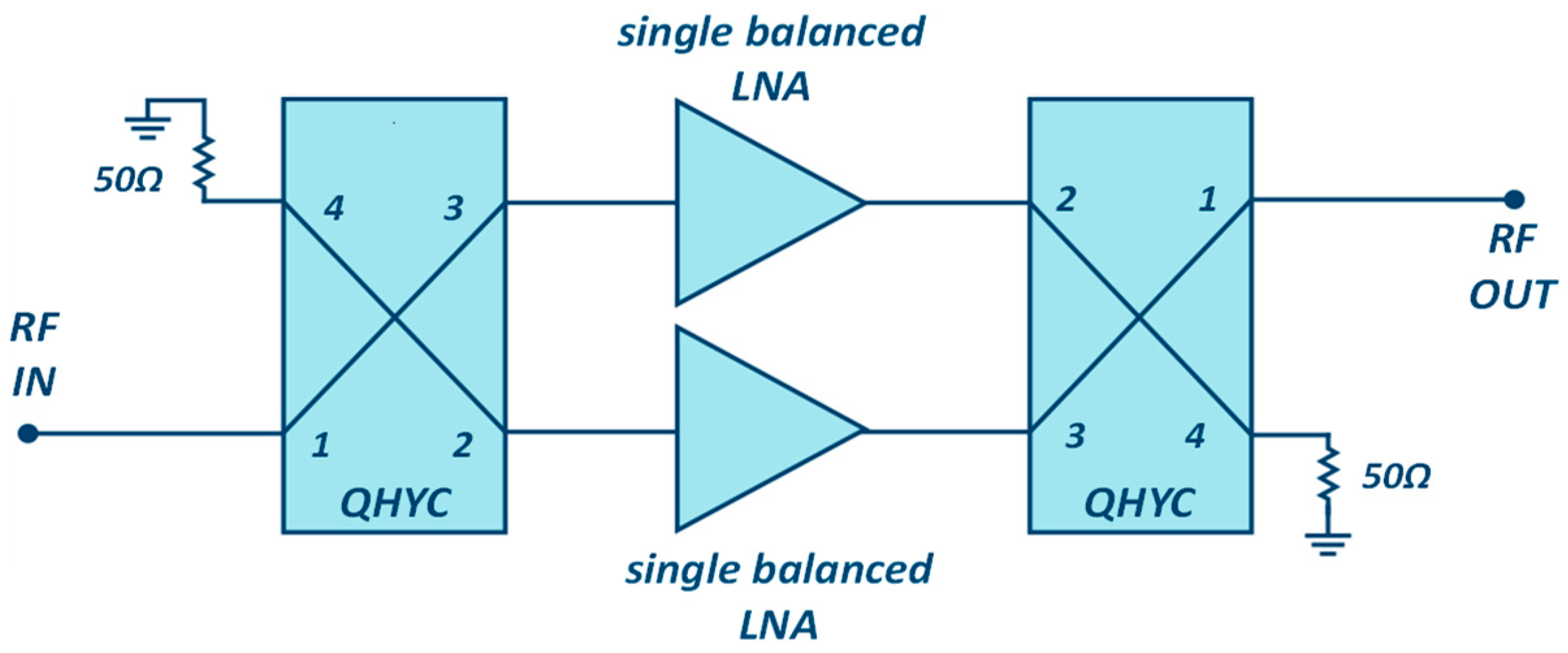
3.3.3. Balanced
Balanced topology represents an interesting solution when adequate values of input and output return loss are required over a very large operating bandwidth. The main downside of this topology is the ohmic losses introduced by the input power splitter that directly affect the mmw-LNA’s NF. Another negative side effect is the size of this circuit, which is practically double the single-ended version. Apart from adequate return loss over a wide operating frequency, this topology has another benefit such as higher power handling capability, since the incident RF power is halved at the input before the two LNA stages. A simplified description is reported in
Figure 9.
The single balanced LNA stages are synthesized as described in
Section 3.1.1., while the input and output power splitter/combiner are quadrature hybrid couplers (QHYC). When used as a divider, the signal is fed at port 1. Consequently, the signals at port 2 and port 3 have ideally identical power (3 dB less than at the input) and are out phased by 90°. Port 4 is isolated, at least ideally, and terminated on the reference impedance (50 Ω). When used as a combiner, ports 2 and 3 act as input ports while port 1 is the output port. Since the signals incident at port 2 and port 3 are appropriately out-phased, the signals are coherently summed at port 1. Once again, port 4 is terminated on the reference impedance (50 Ω) and the two incoming signals are cancelled since they are practically out phased by 180°. An example of balanced mmw-LNAs operating at W-band is reported in [
16,
17]. It is interesting to note that the two realizations only have the circuit topology in common. In fact, while [
16] is a three-stage circuit realized in microstrip InP technology, [
17] is a four-stage realized on GaAs substrate in coplanar-waveguide.
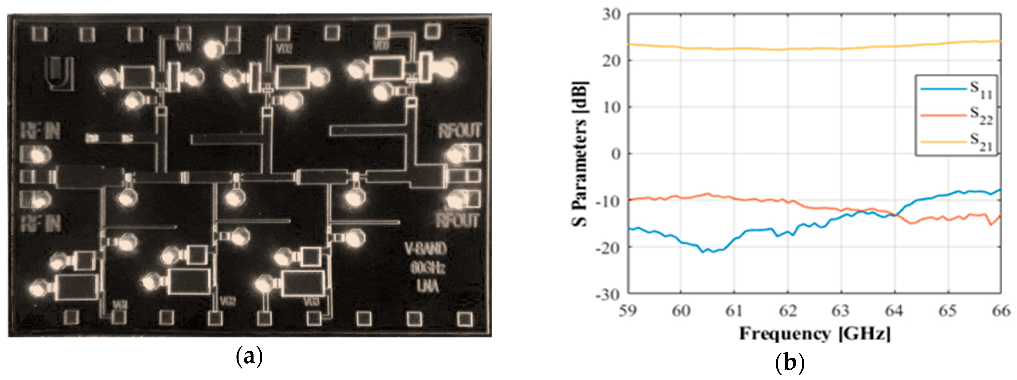
4. Recent State-of-the-Art Implementations
The design solutions outlined in this paper where used to synthesize an mmw-LNA operating in V-band, and more precisely in the 59−66 GHz frequency range. A drawback of V-band (50−75 GHz) is the high attenuation around 60 GHz, due to the absorption of oxygen molecules in the atmosphere, making it impractical for telecommunications that include a terrestrial segment. On the other hand, such absorption is not present in outer space, and V-band represents an interesting option for high-data rate inter-satellite link (ISL) communications.
The mmw-LNA performance requirements (average NF < 2 dB and linear-gain > 20 dB) are challenging considering the working frequency and the limitation of using space-qualified industrial grade technology. Given these constraints, the choice fell upon OMMIC’s D007IH process. A representative device of this technology features around 1.2 dB minimum noise figure (NF
min) at 60 GHz, with 10 dB associated gain [
10].
A single-ended three-stage LNA topology was chosen given the capability of the selected technology and the relatively small bandwidth requirements, which represents a satisfactory trade-off to simultaneously meet the electrical requirements, size, and circuit complexity with the consequent reliability of the circuit. An active device geometry of 4 × 12.5 µm was chosen for all stages. A low-noise operating point was selected: VDS = 1.0 V and ID = 10 mA, and the small-signal and noise model was extracted in-house.
Inductive source degeneration technique has been applied to every stage, as described in
Section 3.3.1, to ease the unavoidable compromise between low-noise and gain.
Figure 10 reports the micro-photograph of the realized mmw-LNA and the measured S-parameters that are in-line with the proposed requirements. Preliminary noise characterization of the LNA has been carried out showing the circuit meets the prescribed requirement: NF < 2dB.
Stability has been analyzed from 1 to 70 GHz using the geometric stability factor of a two-port at its source and load terminals. This value is always greater than unity over the entire frequency range and greater than 1.2 from 23 to 65 GHz.
Regarding the LNA’s non-linear characteristics, the expected output power at 1 dB compression point is +5 dBm, while the output third order intercept point is +15 dBm.
A summary of the key-parameters—operating frequency, average in-band gain, noise figure at room temperature, equivalent noise temperature (T
eq) in cryogenic environment, technology, and propagation structure (GCPW or microstrip)—for recently published mmw-LNAs in open literature is presented in
Table 2.
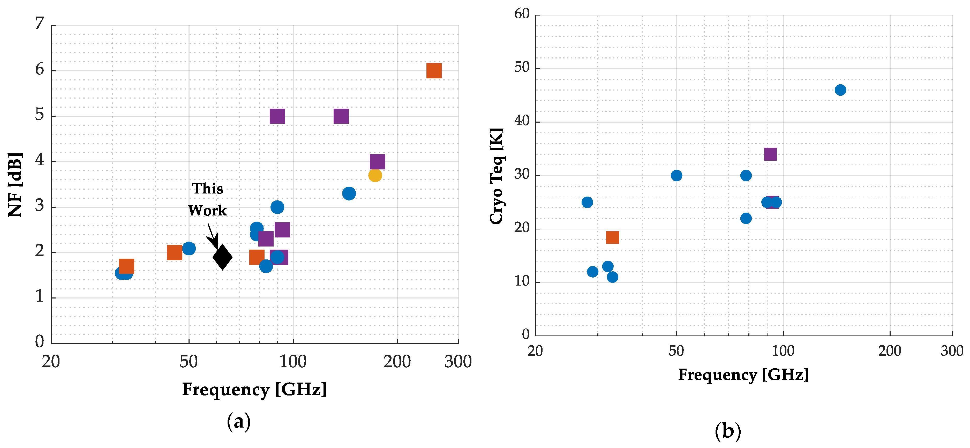
Data are also plotted in
Figure 11, to evaluate the trend vs. frequency and infer an outlook on operation beyond 300 GHz.
The two plots presented in
Figure 11 illustrate state-of-the-art NF and T
eq performance below 3 dB and 35 K up to 100 GHz. Microstrip InP technology is the most common and reveals the best performance in the table, with MMICs exhibiting minimum NF below 2 dB even in the 80−90 GHz band. The presented V-band LNA features 1.9 dB average NF, thus belonging to the state-of-the-art picture.
Regarding room temperature operation, state-of-the art LNAs operating above 80 GHz demonstrate noise figure performance vs. operating frequency quantified through relationship:
where
f0 is the operating frequency, expressed in GHz, while
NF0 is approximately equal to 0.02 dB/GHz. In fact, LNAs operating around 100 GHz demonstrate 2 dB NF, 4 dB NF at 200 GHz and 6 dB at 300 GHz. It is interesting to note that such a linear relationship is verified up to 650 GHz [
42].
Similar considerations apply for the equivalent noise temperature measured in a cryogenic environment. For this feature, the gradient of the linear relationship in approximately 0.3 K/GHz. In this case, results are more spread since the physical temperature at which the MMIC is cooled down influences the equivalent noise temperature. As anticipated in
Section 3.2, MMICs operating above W-band are synthesized using a coplanar waveguide structure, while the microstrip is the preferred choice up to W-band. Finally, the vast majority of the reported MMICs feature a single balanced topology, demonstrating it is a viable solution to obtain low noise and high gain at millimeter-wave.
5. Future Trends and Emerging Technologies at Millimeter-Wave
GaAs and InP will remain the principal semiconductor technologies for very low-noise applications in the future, but the advent of gallium nitride (GaN) or even silicon germanium-based CMOS will modify the scenario within the next 5 to 10 years. GaN has the advantage of providing interestingly low-noise performance in conjunction with very high-power handling capability [
43]. It could become the reference semiconductor for those applications where linearity is a concern together with the robustness to strong interference signal.
Silicon–germanium-based BiCMOS remains somewhat behind for noise performance but has on its side its relatively inexpensive production process that makes it attractive for large-volume applications. In this context, transistors have been realized that exhibit fT and fMAX in the order of 300 GHz/500 GHz.
Further improvements rely on the continuous scaling of the transistor gate length moving towards 10 nm gate length or even shorter devices. Correspondingly, ad-hoc device characterization and modelling will be required to fully exploit device potentials.
Although the topic has not been addressed in this review, packaging at millimeter-wave [
44] can provide further advancement. It will enable more compact/lightweight systems to be capable of operating in harsher environments.
6. Conclusions
The leading technologies and design solutions to obtain millimeter-wave low-noise amplifiers with solid-state devices are presented in this work. InP HEMTs achieve the best noise figure values reported to date. Analysis has demonstrated that a linear LNA NF versus operating frequency is applicable from around 80 GHz up to 650 GHz. Nonetheless, GaAs mHEMTs represent an attractive solution if a (slightly) worse noise behavior is acceptable in exchange for lower cost and higher volume production. In this context, an mmw-LNA operating at V-band has been designed, realized, and tested demonstrating results in-line with the state-of-the-art. Applications for MMIC LNAs at millimeter-wave include radio astronomy, remote sensing, spaceborne communications, short-range high-capacity links, earth science, radar, imaging, vehicle guidance, and security.


