1. Introduction
The electroencephalogram (EEG) experimental and clinical monitoring technique is used for long-term monitoring of the brain’s electrical activity. EEG is a non-invasive and painless diagnostic test, which allows measuring the electrical activity of the brain by simply placing several electrodes on the head (scalp) around the brain. The potential differences measured from sets of two electrodes are converted into waveforms. These signals are used to evaluate the brain disorders in epileptic patients representing our interest. Recently, there was an increasing demand of miniaturized biopotential acquisition systems. These systems are lightweight, portable, do not hinder patient’s mobility, and are comfortable to the patient during the monitoring. The EEG signals are difficult to be measured due to their extremely weak amplitude, in the range of 1–160
V
PP, and their limited band to a very low-frequency range from 0.1 to 100 Hz. Therefore, the EEG acquisition systems are susceptible to ambient noise (50/60 Hz common-mode interference signal coupled to human body from the mains), amplifier flicker noise (
), and DC offset, as well as to problems of electrode DC offset generated at the skin-electrode interface and between electrodes. This can lead to the saturation and reduction of the CMRR of the readout front-end that defines the quality of the extracted signal [
1]. To extract a high-quality EEG signal under the above-mentioned conditions, low-power, low-noise, and high-CMRR and PSRR readout front-end are needed. In the remaining parts of the paper, we introduce the state-of-the-art on the front-ends dedicated to EEG signal acquisition. The proposed EEG acquisition channel is presented in
Section 3, followed by a detailed explanation of the design and implementation of the LPGA.
Section 4 shows the measurement results of the LPGA prototype integrated in 180 nm CMOS process. Conclusions and future work are given in
Section 5.
2. Background and Previous Work
The amplifier in [
2] consists of a low-noise closed loop amplifier (LNA) including a chopper stabilization module and a GM-C servo-loop to cancel offset current. Resistances and capacitances components are used off-chip. However, these off-chip components and the transconductor of the servo-loop increase the overall noise of the instrumentation amplifier. Furthermore, the amplifier provides low CMRR (60 dB) even at higher input-impedance and low-voltages operation. This is because of performing the input modulation at the op-amp virtual ground node. Additionally, mismatch in the input capacitors can convert common-mode input signals to differential-mode noise. Low-noise, low-offset, and large-output voltage swing amplifier design is introduced in [
3]. It consists of AC coupled chopper folded-cascode amplifier combined with an input-impedance boosting loop and two offset trimming loops based on auxiliary current DACs for input offset and residual offset cancelation. A back-end common-mode feedback (CMFB) circuit is designed to improve the CMRR of the active electrode system. However, the CMRR of the CMFB circuit is limited by the electrode-tissue contact impedance mismatch. In addition, the use of these many active circuits (to solve offsets, ripple, input impedance problems and CMRR enhancement) reduces the SNR and increases the integration area. Recently, AC-coupled non-inverting chopped two-stage IA followed by a transconductance amplifier (TA) is reported [
4]. The input pair of the IA consists of NMOS and PMOS differential pairs connected in parallel, which reduces the thermal noise of the input-referred voltage-density and doubles the input transconductance of the core amplifier without consuming extra bias current. Besides, the above design provides voltage gain, high input-impedance, low noise, and the ability to reject large electrode offset. However, the main drawback of the presented IA topology is the lack of CMFB circuit, which gives in the common-mode output variation of the TA. This results in a high-output distortion, low CMRR and PSRR, and high offset voltage. Moreover, the use of two amplifiers increases the IA noise. To adequately amplify the low EEG signals with a dynamic range of 80 dB and compress the largest ones created during the epileptic crises, we present in this paper a low-noise and high-CMRR rail-to-rail logarithmic programmable gain amplifier (LPGA) as well as a chopped LPGA (CLPGA) dedicated to EEG acquisition channels/systems.
3. The Proposed System
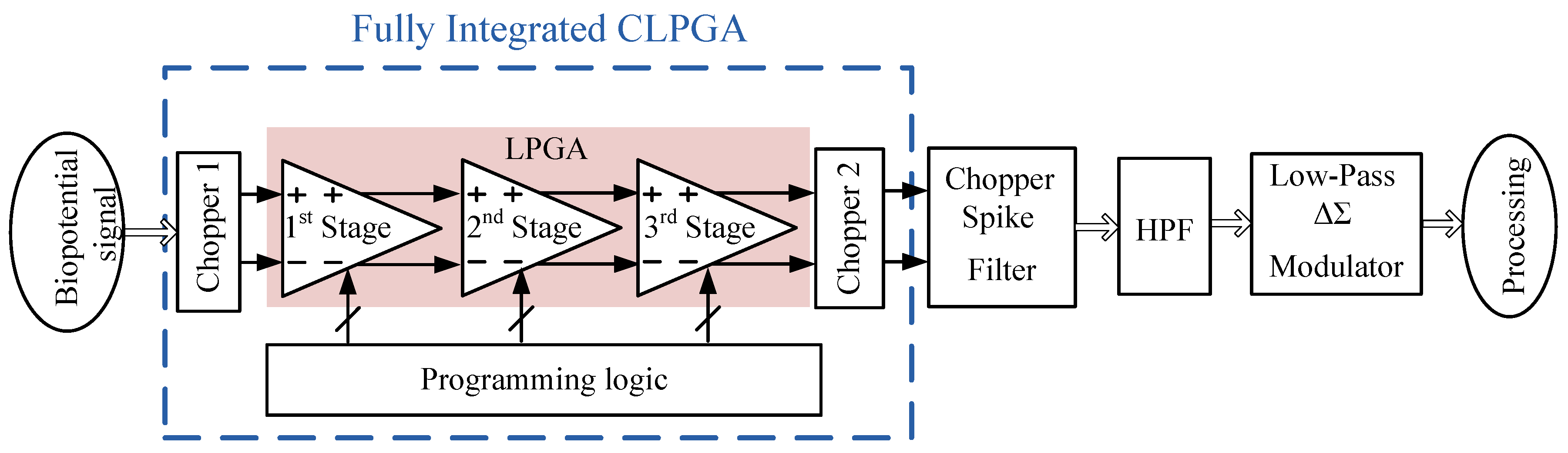
Figure 1 shows the architecture of EEG acquisition system, where the proposed fully integrated CLPGA is used as pre-amplification stage [
5]. A high-pass filter is employed to cut off all received signals with frequencies lower than 0.1 Hz. In addition, a high resolution (up to 14 bits) delta-sigma modulator is used to digitize the amplified signal. This high-resolution modulator maximizes the number of available quantization steps, while reducing quantization noise error and increasing signal-to-noise ratio (SNR ≥ 100 dB). In addition, the proposed design involves a gain-programming logic to fit the EEG signal into ADC’s input dynamic range. The
noise is reduced in the proposed CLPGA by using large size PMOS and NMOS input pair transistors and applying a chopper stabilization (CS) technique [
6,
7]. Chopper 1, which is based on CMOS switches, is used to transpose the EEG signal to 1 kHz chopper frequency to up-modulate the
noise to a higher frequency further away from the signal band [
8]. Chopper 2 acts as demodulator to place back the amplified EEG signal on its original band.
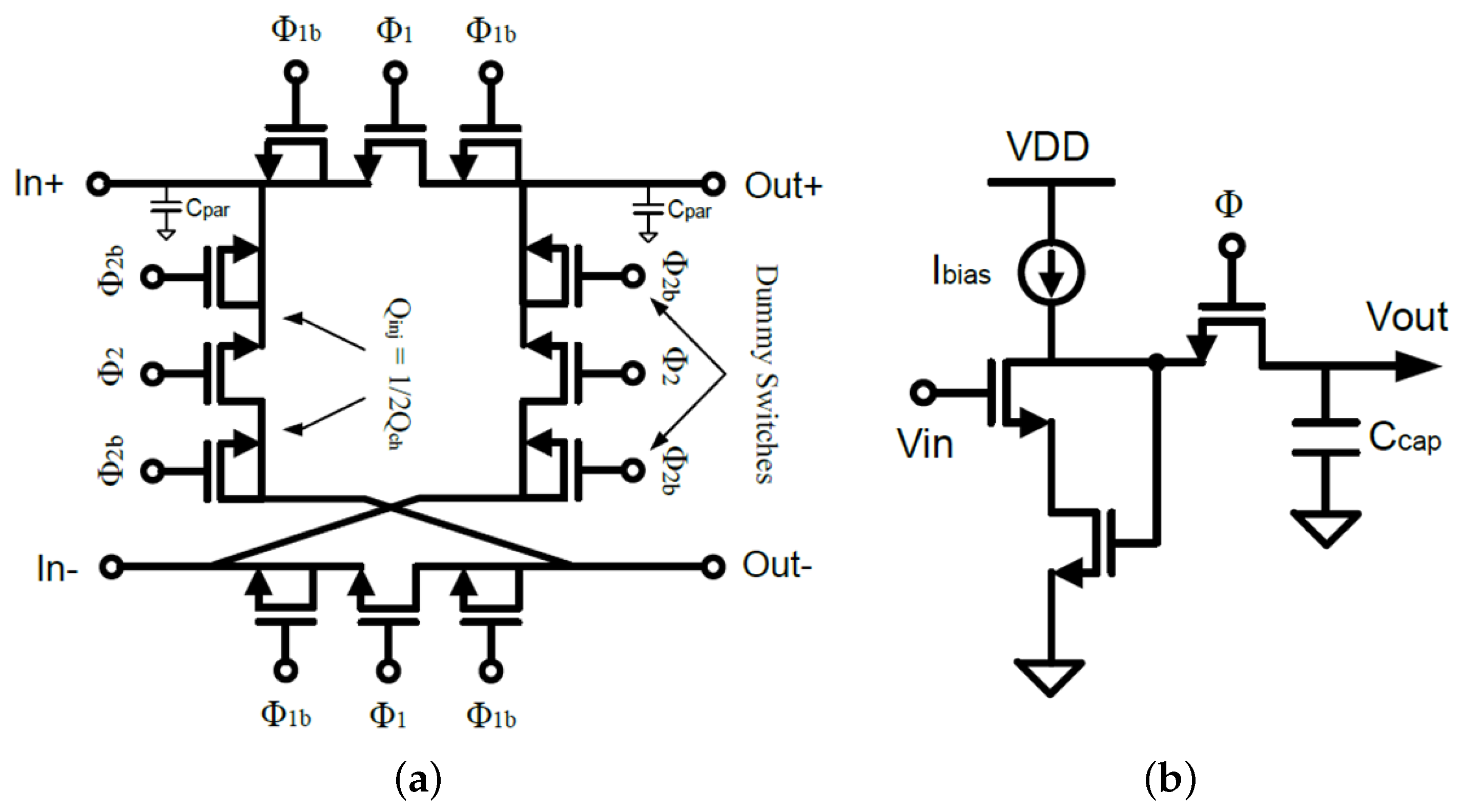
Figure 2a shows the circuit implementation for Choppers 1 and 2, where dummy transistors have been added to reduce the generated spikes from the chopping process (due to charge injection from the used switches). In addition, a chopper spike filter shown in
Figure 2b has been used to cancel these spike voltages. Our work in this paper focuses only on the design, implementation, and experimentally validation of the LPGA circuit.
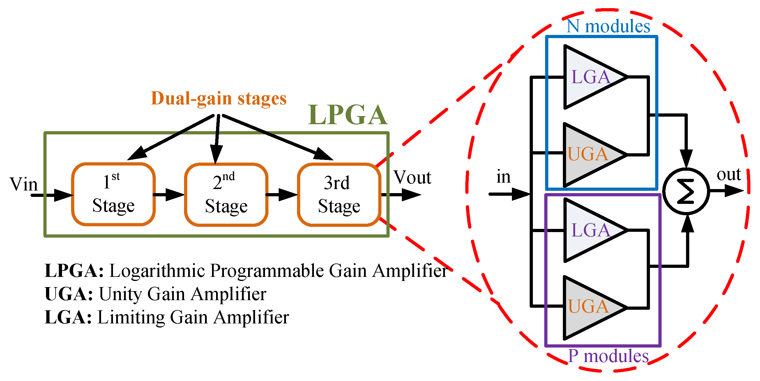
3.1. LPGA
Figure 3 shows the block diagram of the proposed rail-to-rail LPGA. It is based on a differential topology of true logarithmic amplifier (TLA), where the phase shift or group delay does not vary with the input signal level. The LPGA consists of three cascading rail-to-rail dual-gain stages. To achieve high CMRR, low noise, and low offset in a wide-input common-mode range, each stage is composed of chopper-stabilized parallel N and P type modules, where their differential outputs are added together to perform logarithmic function. Depending on the input common-mode range, only one chopper-stabilized module is active at any time. The N type module is active when the input common-mode voltage is from 0 V to VDD. P type module is active when the input common-mode voltage is from VSS to 0 V. The gain of each stage consists of two parallel amplifications: limiting gain amplifier (LGA) and unity gain amplifier (UGA). LGA treats the signals that have the amplitude lower than a threshold input voltage (V
iL) and limits the output voltage (V
oL) when the amplitude of the input signal is higher than or equal to V
iL by the following equations:
where A, V
iL, and V
oL are the gain of the LGA, the input limiting voltage, and the output limiting voltage, respectively. Usually, for the UGA,
. Thus, the output voltage of one dual-gain stage is given by:
where
is the linear part of a dual-gain stage. Consequently, the linear gain of the cascaded three stages is equal to
. The output voltage characteristic consists of a series of straight lines with breaking points indicating each limiting amplifier stage. Assuming n cascaded dual-gain stages are used and knowing that the limitation comes from the mth stage towards the
th stage of the TLA, the output of the mth stage (V
om) of the TLA is given by:
The expected signal passed through n−m limiting stages, Equation (
5) applied for each stage, gives the following:
The input of the m-th stage (V
in,m) at the beginning of the limitation is amplified by m − 1 stages and given by:
Substituting Equation (
6) into Equation (
4), we find
Equation (
9) demonstrates that the output signals follow the suited logarithmic variation. Given that the linear gain and the precision of the LGA are determined by all involved stages, 14.67 dB gain by one stage is required. Therefore, three stages are needed to obtain a 44 dB gain by the TLA. Each dual-gain stage is based on a differential circuit used to reject the input noise coming from the previous stages.
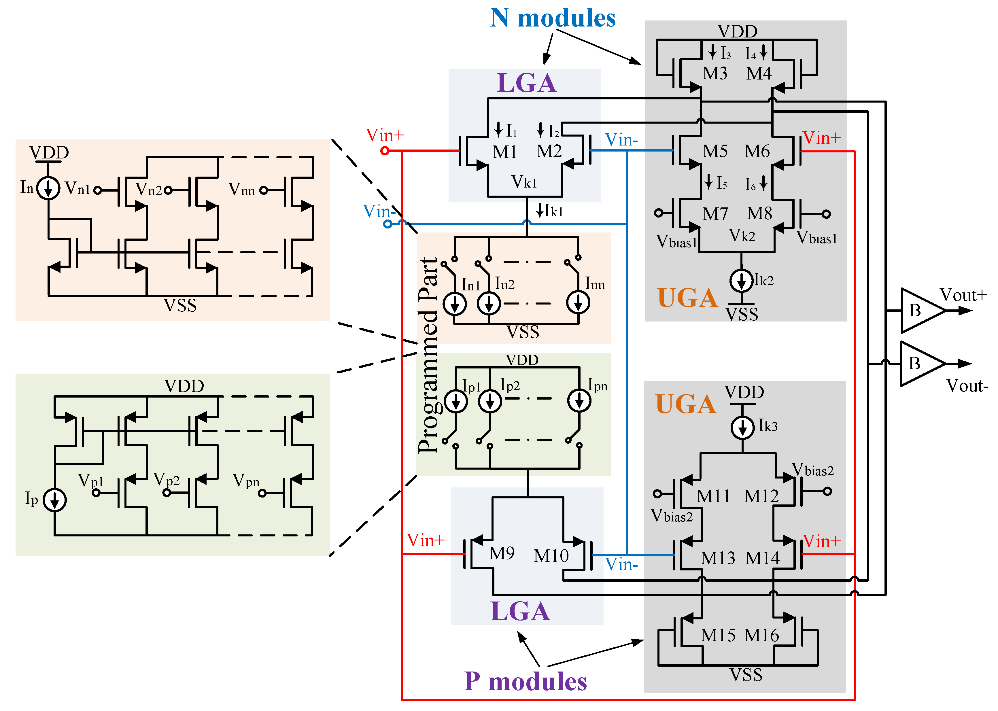
Figure 4 shows the circuit implementation of the differential rail-to-rail topology for one dual-gain stage. Both LGA and UGA circuits share M3 and M4 transistors, which are used to produce the gain limitation or blockage of differential pairs composed of M1 and M2. The UGA stage, defined by M7 and M8 transistors, is working in the triode region as resistances. The ratio of bias currents I
n and I
ntotal, I
p, and I
ptotal depends on the number of stages cascaded in order to get the desired dynamic range. The identical transistors M3 and M4 determine the limiting gain (2A), which dominates the total gain of one dual-gain stage 2(A + 1). The sizes of these transistors are chosen to be large to get the adequate gain for each stage. M1 and M2 constitute the input differential pair of the LGA, while M3 and M4 represent the active load, and M5 and M6 form the input differential pair of the low transconductance UGA. Output currents of both LGA and UGA are added together; I
k1 is the LGA bias current and I
k2 is the UGA bias current. The LGA and UGA gains are linear and the transistors of their input differential pairs work in the saturation region when the amplitude of input signal is very low. However, when the amplitude of the input signal is large, one transistor of the differential pair will be off and the bias current will be drained through the other transistor. The output of LGA will be limited by the drain-source saturation voltage of transistors M3 and M4. At breaking point:
where
corresponds to the transconductance’s constant of transistor
and
is the threshold voltage. Therefore, VIL can be set by designing Ik1 and Ik3 through the aspect ratio of M3, M4, M11, and M12.
Rail-to-rail output stage (Buffer B), which is realized by class-AB configuration, is connected at the output of the last stage of the LPGA to achieve low-output distortion and therefore getting the maximum SNR at the output [
9].
3.1.1. CMRR
The CMRR is the important critical parameter of the amplifier to be enhanced to reject the mains interference. Usually, to improve the CMRR of the EEG channel, a driven right leg (RLD) circuit is used to feed a common-mode signal to the patient body to cancel the interference [
10]. This method effectively reduces the common-mode gain and increases the CMRR. However, this kind of loop is difficult to stabilize due to the uncontrollable electrode-tissue impedance of the dry electrodes. To solve this problem, a digital RLD circuit has been presented in [
11] to provide a high common-mode signal reduction at power line frequency. However, this circuit requires additional modules such as notch filter, digital signal processing and digital-to-analog converter, and hence greater power dissipation. Another technique to improve CMRR is the use of common-mode feedback [
3], i.e., to feed the common-mode signal back to the input of each preamplifier. However, the feedback loop requires a summing amplifier and large compensation-capacitors for common-mode extraction and stability. This results in large silicon area. In this work, the presented LPGA is formed by cascading three amplification stages, where the CMRR (dB) of the overall LPGA can be expressed by [
12]:
Thus, a very-high CMRR can be achieved. In addition, the PSRR will be increased since it is directly related to the gain [
12]. To further improve the CMRR, the common-mode gain (
) of the logarithmic amplification topology must perform very-high attenuation on all common-mode signals applied at the input of the LPGA module.
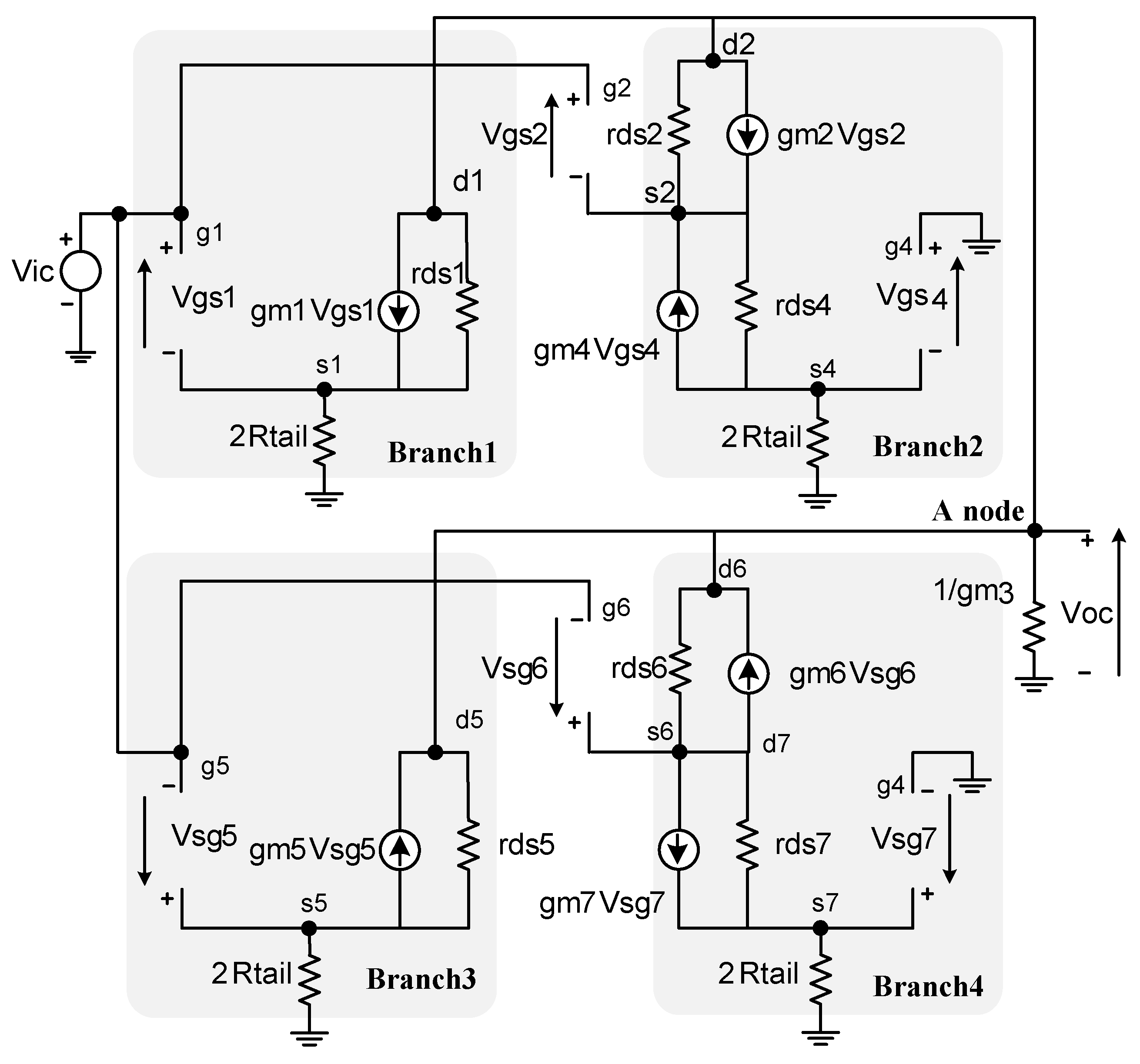
To calculate the A
cm of the perfectly balanced differential amplifier shown in
Figure 4, its small-signal equivalent half circuit is extracted, where we ignored the body-effect transconductance (gmb) [
13]. However, as this perfectly balanced amplifier is symmetric, the calculation is greatly simplified by using the superposition theorem on the circuit shown in
Figure 5. Firstly, we found the responses to the small signal currents in term of the pure common-mode input V
ic of each branch, and adding all currents at summation node A to obtain the total common-mode gain A
cmTotal, i.e., A
cmTotal = V
oc/V
ic. For the four branches of the circuit of
Figure 5 and considering our optimization of this circuit, the values of r
ds1, r
ds2, r
ds5, and r
ds6 are very small and for ideal case g
m1 = g
m5, g
m2 = g
m6, and g
m4 = g
m7. Thus, the drain currents of each branch can be expressed by:
where I
ds1 = −I
ds5 and I
ds2 = −I
ds6, thus I
ds1 + I
ds2 = −(I
ds5 + I
ds6). Consequently, the total common-mode gain at the summation node A can be expressed as
where g
m3 is the transconductance of the active load of each stage and A
cm1 and A
cm2 are the common-mode gain of the N modules and P modules, respectively.
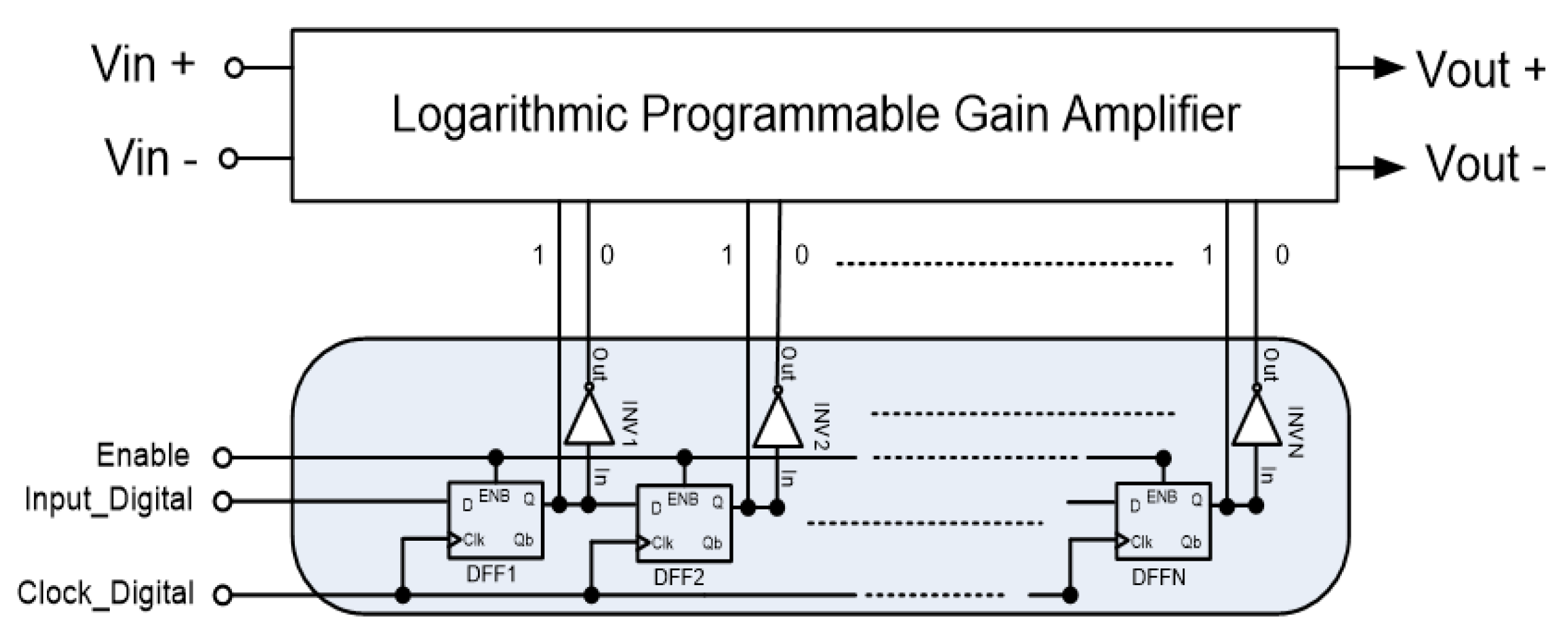
3.1.2. Programming Logic
To fit the EEG signal into ADC’s input dynamic range, a programming approach is proposed which is based on the variation of the tail current transistor width of each stage. To program the gain of the one dual low-gain stage, the tail currents of the N and P type LPGA stages must be reduced consecutively. By turning off the switches of In1 and Ip1 in the programming ladders, the node voltage (Vk1) increases, Vgs1/Vgs2 decreases, Vds1/Vds2 increases, Vgs3/Vgs4 decreases, and I1, I2, I5 and I6 decrease. Accordingly, the gain A and the dynamic range
decrease. The logic diagram shown in
Figure 6 is employed to program the gain of the LPGA. It has been implemented using a shift register, which receives a series input and produces n parallel outputs to tune the N modules. In addition, complementary n outputs have generated (through inverters) to tune the P modules.
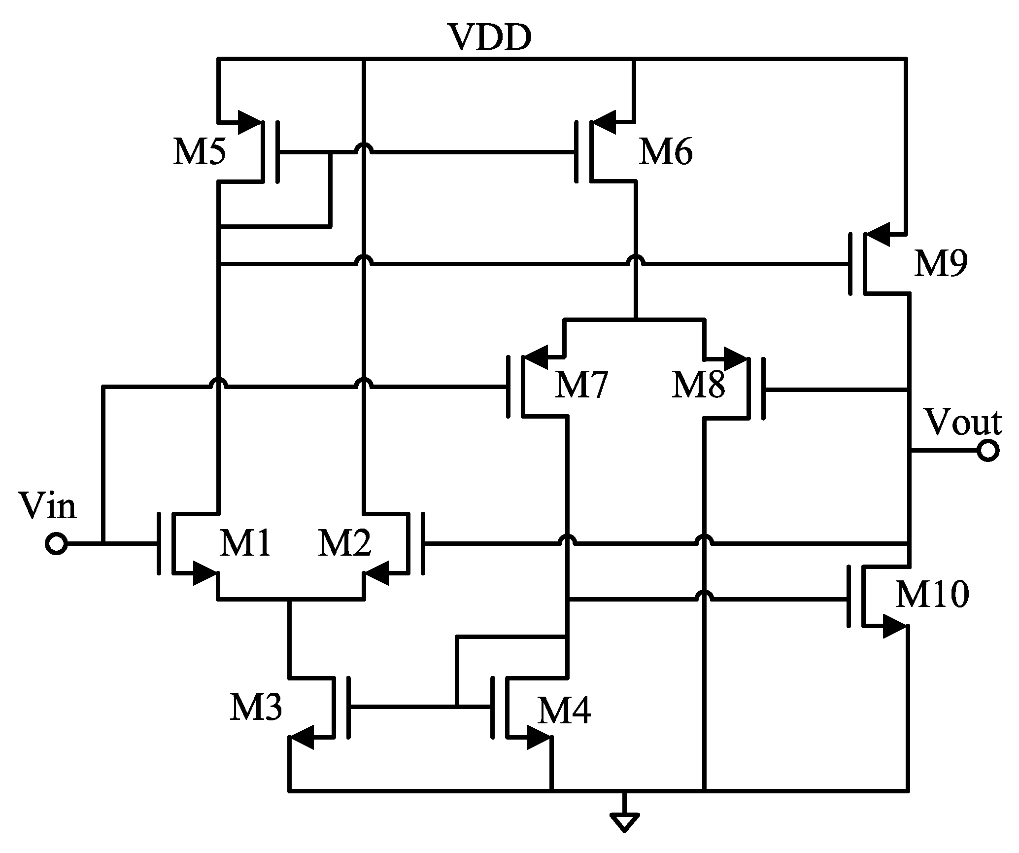
3.1.3. Rail-to-Rail Output Stage
To get the maximum SNR at the output, the LPGA is required to achieve a rail-to-rail output swing, which is realized by class-AB architecture shown in
Figure 7 and connected at the output of the last stage of the LPGA. This architecture consists of two transconductances (
,
) and a pair of complementary common-source amplifiers (M9 and M10). The output is connected to the inverting input terminal (Vout) and the input signal is applied to the non-inverting input terminal (Vin). It is noted that the small resistors of the demodulator’s switches, in which the LPGA needs to drive them, make the primary motivating factor to use class-AB buffer as output stages to achieve low-output distortion [
14]. M2 and M8 are directly connected to VDD and GND, respectively, to have an active load of zero, thus not amplify the feedback signal. The balancing of the bias currents for the differential pairs is done by means of the feedback topology. When the non-inverting input voltage is decreased, the gate voltages of M9 and M10 are increased. As a result, M10 starts to discharge the output node. When the output voltage reaches the level that the voltage difference between the input and output is almost zero, M10 stops discharging the output node [
14]. Similarly, when the input voltage (Vin) is increased, M9 charges the output load until the output voltage almost equals the input voltage. The single-ended amplifier incorporates a complementary differential pair as the input stage does, to obtain a full input voltage swing.
4. Measurement Results
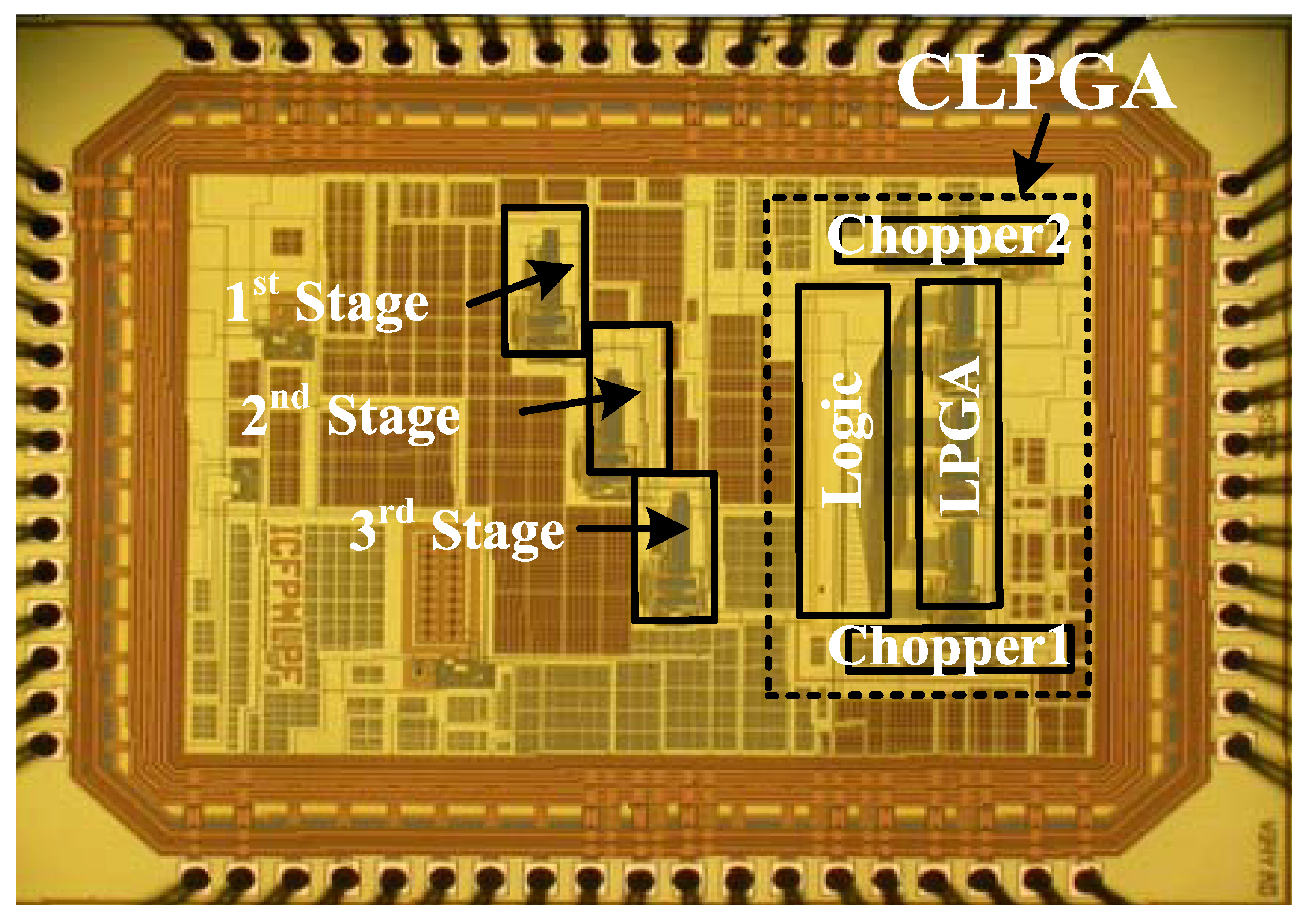
A die photograph of the proposed LPGA and CLPGA circuits implemented in TSMC 180 nm CMOS process is shown in
Figure 8, where they occupy an active area of 0.4 mm
2 and 0.52 mm
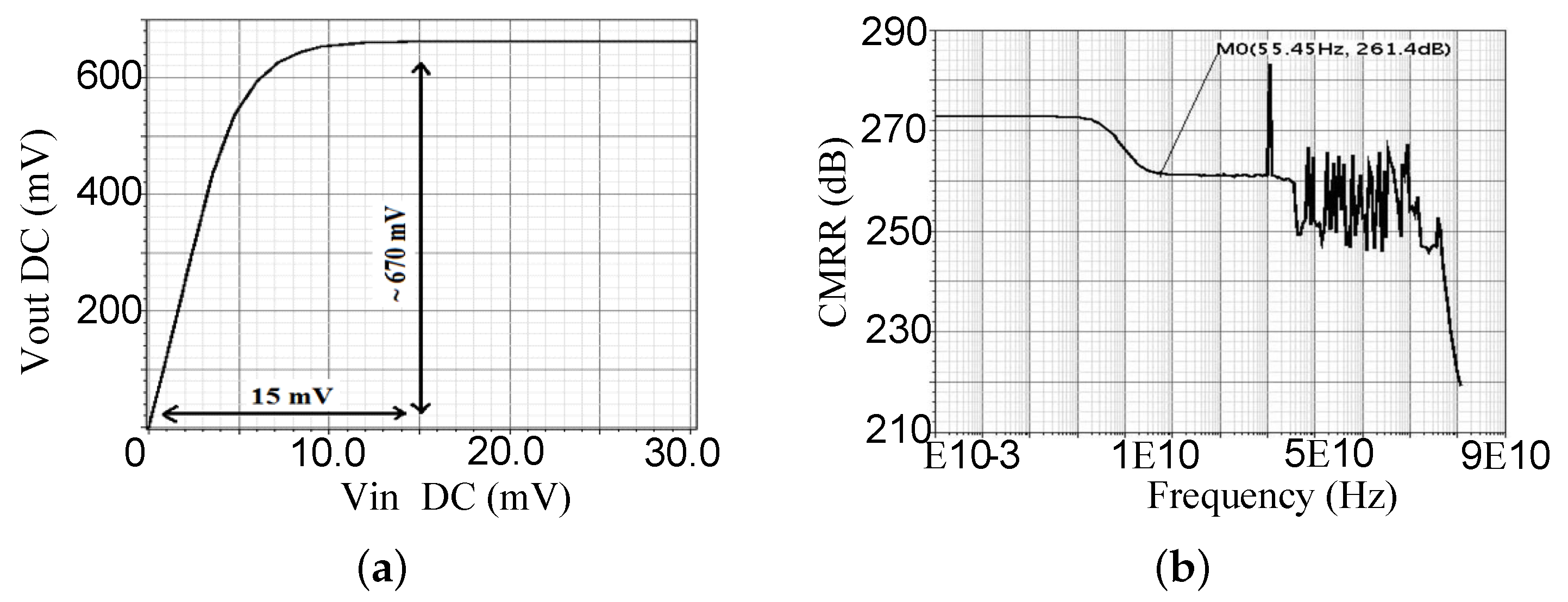
2, respectively. The post-layout simulations were done with Spectre under Cadence platform, and the fabricated chip was tested in our Polystim Neurotech Laboratory. The DC transfer function of the CLPGA is shown in
Figure 9. For an input DC voltage of 15 mV, the simulated output DC voltage is approximated as 0.67 VPP.
Figure 9a demonstrates the simulated transfer function of the CLPGA, while the bode transfer function of the simulated CMRR is shown in
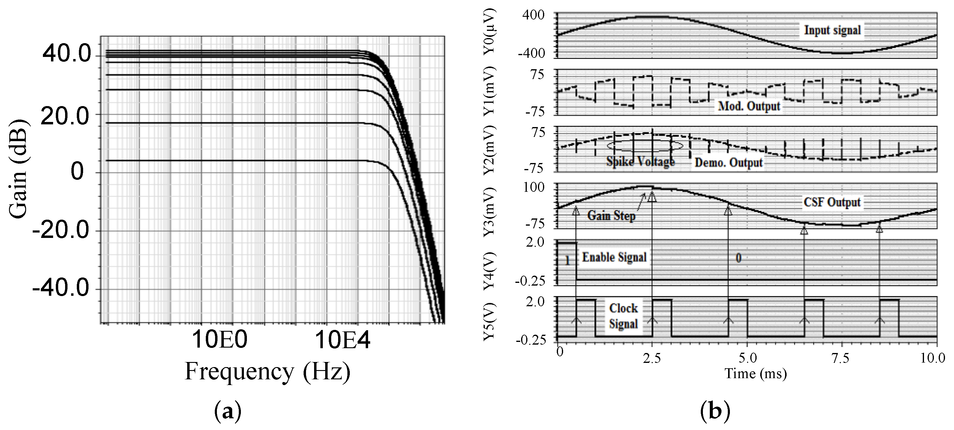
Figure 9b. The simulated values depict the high ability of the CLPGA to reject the common-mode interference (50/60 Hz) ambient signal coming from the main source coupled to the patient’s body as well as any signal noise and DC offset electrodes applied to CLPGA differential input. Simulation results of the CLPGA bode transfer for different gains at 1 dB step and for a maximum gain of 44 dB are presented in
Figure 10a. The transient simulation results are given in
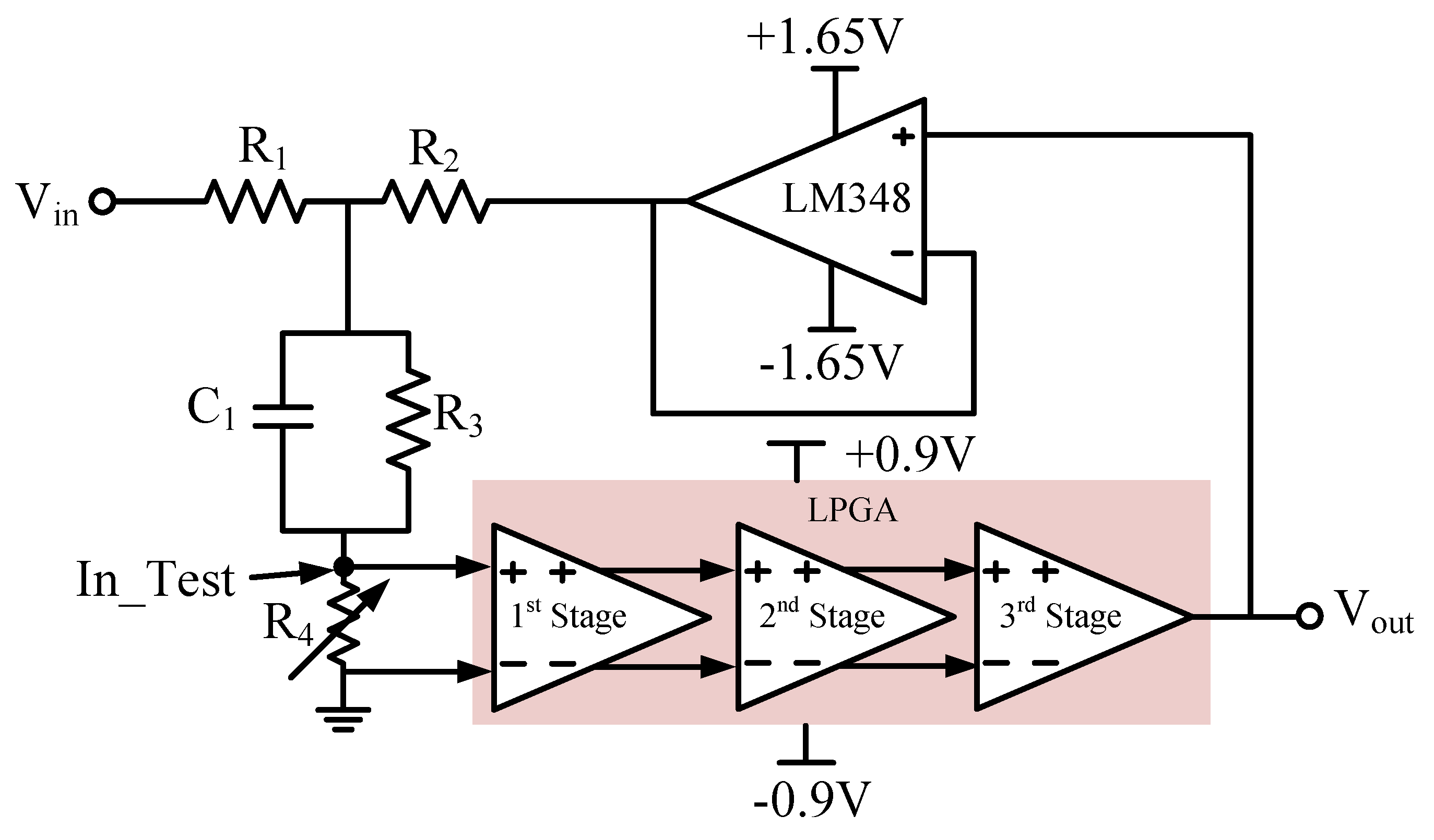
Figure 10b, which shows the step-down output magnitude of the CLPGA controlled by the digital part at each rising edge of the clock signal right after the falling edge of the enable signal as well the spike voltage due to charge analog switches. The chopping frequency is 1 kHz, while 0.5 kHz clock is used for the chopper spike filter. The measurements have been performed in a closed-loop configuration shown in
Figure 11 [
15,
16]. Based on this method, the LPGA is configured with a signal gain of −1 V/V using R
1 = R
2 = 10 k
and the LPGA has been supplied by ±0.9 V and it is acting as a preamplifier for its own error signal with R
3 = 1 M
and a variable resistor (R
4) of 2 k
used as a voltage divider at the inverting input. A 20
F ceramic capacitor, C
1, is connected across R
3 to filter the low amplitude error signals from noise. Furthermore, to reduce the effect of finite output impedance of the LPGA-under-test and the effect of feed-through due to the feedback path of the test set-up, a general purpose amplifier configured as a voltage buffer is used in the feedback loop [
16]. Note that the passive elements and the buffer shown in
Figure 11 are off-chip components. The open-loop gain obtained from the set-up is calculated as:
This open-loop gain was measured using a sine wave input of 5 V
PP and a frequency of 100 Hz.
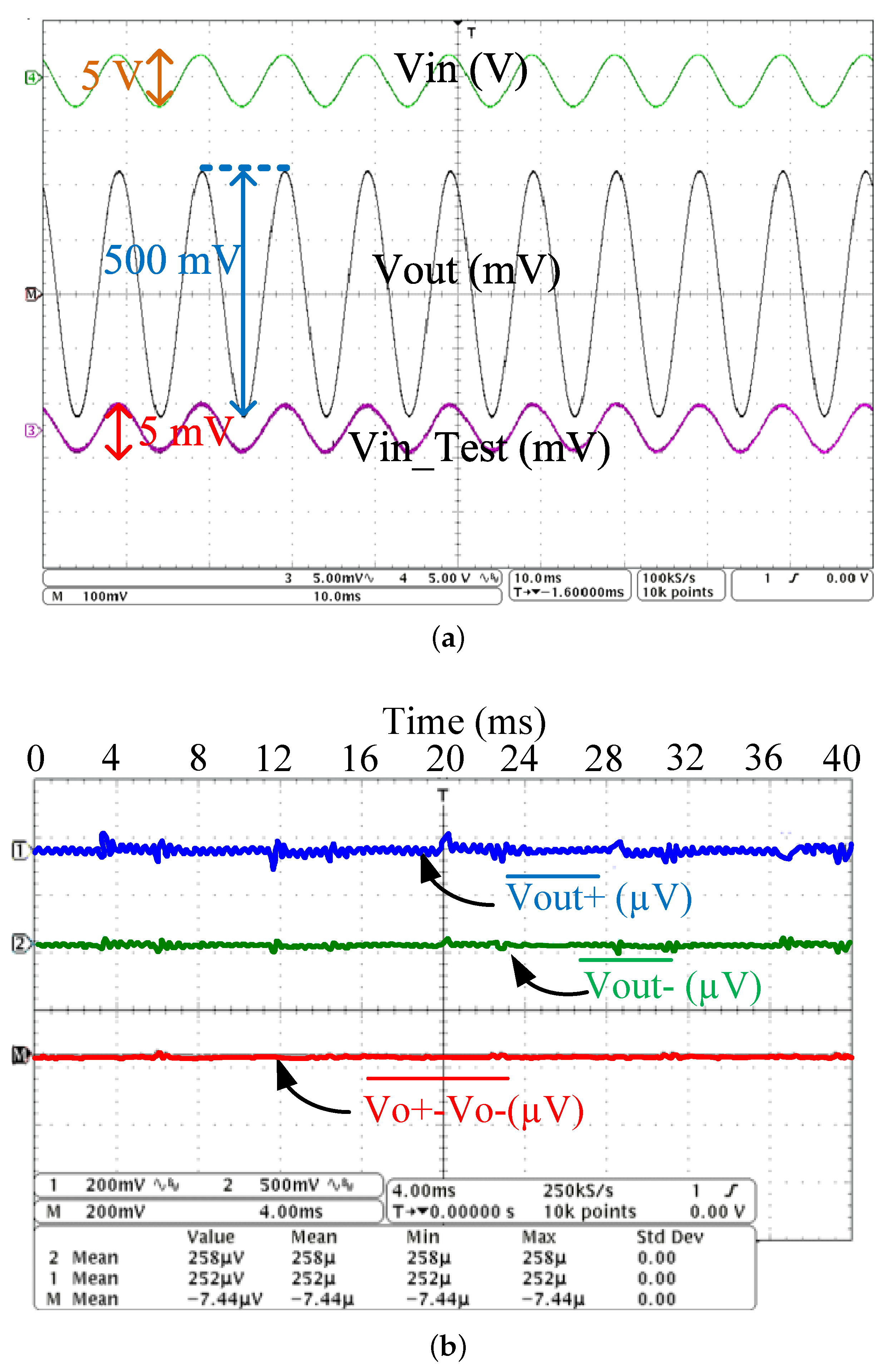
Figure 12a shows approximately 500 mV
PP output signal swing, for the differential input error voltage magnified by a factor of 100, with a maximum value less than or equal to 5 mV
PP. The measured open-loop gain is at least 37 dB at 100 Hz. The CMRR is measured by connecting the differential input of the LPGA to a sine wave of 1 V
PP at 100 Hz.
Figure 12b shows the measured peak-to-peak value of the LPGA differential output, where a 1 V
PP input signal has been applied and we obtained the mean values of Vout+ and Vout−, which are found to be 252
V and 258
V, respectively. Then, the differential signal (7.44
V) is obtained by subtracting Vout+ and Vout−. Therefore, the common mode gain is calculated as 20 Log (7.44
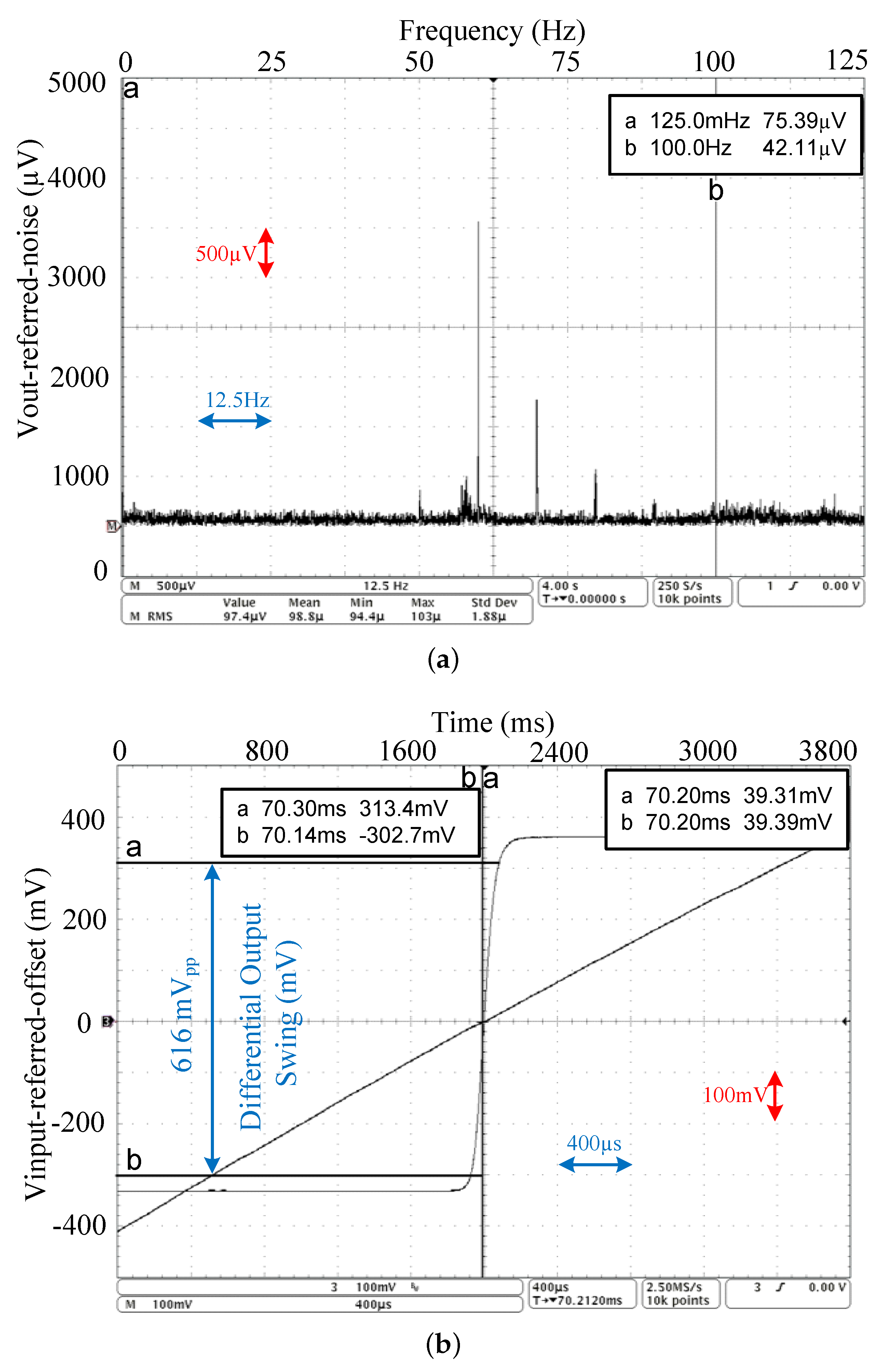
V/1 V), which results in 103 dB. The high CMRR value is the sum of the common-mode gain (≈103 dB) and the differential gain (≈37 dB), making the capacity of LPGA to reject any common noise signal applied to its differential input. The input-referred noise voltage is measured by connecting the LPGA inputs to ground and performing spectrum analysis of the output signal.
Figure 13a shows the measured linear RMS value of the differential output under various input amplitudes and frequencies (75.39
V
rms@ 0.1 Hz, 3 mV
rms@ 50/60 Hz, and 42.11
V
rms@ 100 Hz. Consequently, the measured input-referred noise voltage of the LPGA is determined by dividing the previous values by the linear gain (100 V/V). The input-referred offset voltage of the LPGA is measured by operating the LPGA as comparator and applying a ramp of 1 V
PP at VIN+, and the ground at VIN−. The measured input-referred offset voltage that it must be put on the input VIN+ to set the DC differential output of the LPGA to zero is 78.13
V, as shown in
Figure 13b. In addition, this figure depicts the measured maximum differential output swing of the LPGA, around 616 mV
PP.
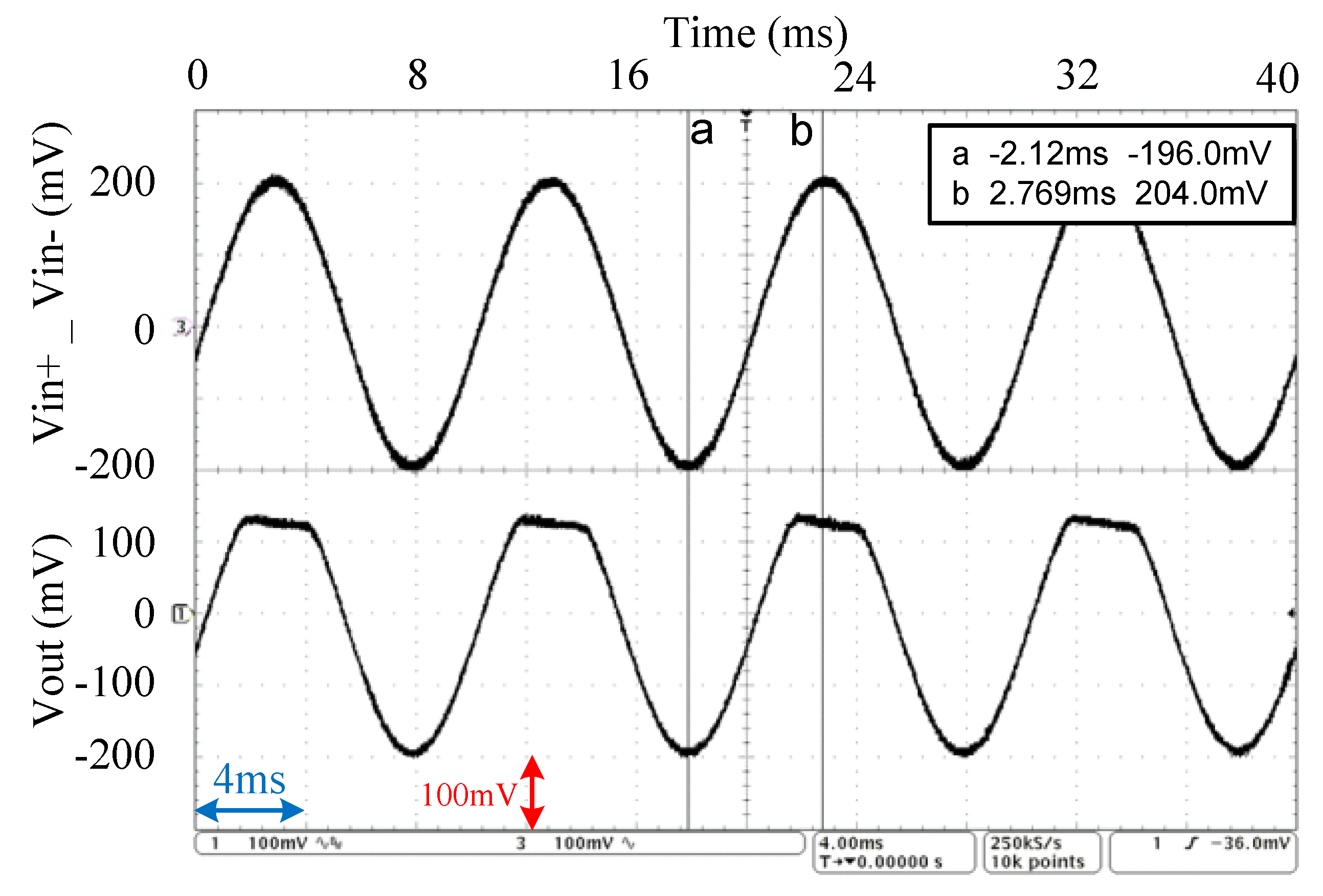
To amplify the signals, grouping offset, detected by the mismatched EEG electrodes and avoid severe distortion in the LPGA performance as well unity gain bandwidth (UGBW) variation, the measured input voltage range of the complementary LPGA can range from −200 to 200 mV, as presented in
Figure 14, where a sine wave signal at 100 Hz is increased gradually at the differential input until the output signal begins to distort. Measurement results of the LPGA are summarized in
Table 1 for a resistive and a capacitive load of 10 M
and 95 pF, respectively. Although the proposed design achieves high-CMRR, it consumes relatively large amount of power compared to similar designs, as a result of using three amplification stages to increase the CMRR. Therefore, and to provide a fair comparison, we considered a figure of merit (FOM), which is the noise efficiency factor (NEF) as shown in Equation (
17) [
17]. The NEF of the proposed design is 29.8.


