1. Introduction
The electronic computing systems developed so far have been structured on the von Neumann architecture in which the memory, the processor, and the controller exist separately, and the sequential processing among them embodies specific functions within the programmed software. Most of the digital and analog circuits included in the memory and processing units are composed of complementary metal-oxide-semiconductor (CMOS) devices that have made a significant contribution to the semiconductor industry. Improvements in the performance of modern computing and information technology are based on the permanent scaling down of the CMOS devices, which provide a cost-effective increase in the operating frequency and a reduction in the power consumption [
1,
2].
Currently, the integration density of CMOS devices do not conform to Moore’s law [
3], and the scaling down is fast approaching the physical limit. However, an increase in the operating frequency and the device density increases the power consumption and the operation temperature, which can seriously degrade the system performance (von Neumann bottleneck), mainly because of the time and energy spent in transporting data between the memory and the processor [
4]. This is particularly noticeable for data-centric applications, such as real-time image recognition and natural language processing, where the state-of-the-art von Neumann systems cannot outperform an average human.
Unlike with the von Neumann systems, the human brain creates a massively parallel architecture by connecting a large number of low-power computing elements (neurons) and adaptive memory elements (synapses). Thus, the brain can outperform modern processors on many tasks that involve unstructured data classification and pattern recognition [
5]. Furthermore, the ultra-dense crossbar array consisting of memristors have been recognized as a potentially promising path to building neuromorphic computing systems that can mimic the massive parallelism and extremely low-power operations found in the human brain [
6]. Representative types of neuromorphic computing schemes are the biologically inspired spiking neural networks (SNNs) and deep neural networks, which are vector matrix multipliers [
7,
8]. The SNNs are based on the local spike-timing-dependent plasticity (STDP) learning rule [
7], whereas the latter is based on the backpropagation learning rule [
8].
The two-terminal binary metal-oxide-based resistive switching (RS) devices, such as HfO
x, AlO
x, WO
x, TaO
x, and TiO
x, have been widely studied as memristor devices that play the role of synapses in the crossbar arrays because the underlying metal–insulator–metal structure is simple, compact, CMOS-compatible, and highly scalable. Indeed, their energy consumptions per synaptic operation and programming currents can be made ultralow (sub-pJ energies, <1 μA programming current) [
9]. However, in most cases of these
filamentary resistive switching random access memory (hereinafter ReRAM) devices, the filament formation/completion process is inherently abrupt and difficult to control. This problem is particularly acute in neuromorphic applications because a single highly conductive device with a thick filament provides much more current to a vector-weighted sum or a leaky integrate-and-fire than its neighbors [
10]. Undoubtedly, the gradual RS characteristics (i.e., the analog nonvolatile memory characteristics of the memristors) are most viable for either the weighted sum operation of convolutional neural networks (CNNs) or the STDP as a learning rule for SNN. In particular, the synapse device using the memristor requires excellent linearity according to the consecutive potentiation/depression pulse for high data processing accuracy [
11].
In the case of filamentary ReRAM devices, there is ambiguity at the boundary between the application of the digital memory device using the abrupt RS operation and the application of the synapse device using the gradual RS operation. Therefore, it is very difficult to optimize each of the devices for both applications in terms of the process and the material. More noticeably, the efficiency and linearity of the resistance modulations of the metal-oxide-based memristors are frequently contradictory to one another when applying the potentiation/depression (P/D) pulses [
12]. This is because when the resistance changes of the filamentary ReRAM devices occur more efficiently (abruptly), the resistances become more nonlinear in relation to the increase in the number of P/D pulses. After being triggered by an electric field and/or a local temperature rise during the SET/potentiation pulse, the filament formation/completion must be cut by an external circuit so that the filament is not too thick to be removed with an accessible RESET/depression pulse. Despite using techniques such as incrementally increasing the amplitude of the P/D voltage and/or increasing the duration of the P/D pulse [
13], the complicated scheme for self-adaptively varying either the amplitude or the duration of the P/D pulse would be significantly compromised with the use of external controls and circuits. This results in additional power consumption and design complexity and seriously dilutes the motivation of neuromorphic computing systems.
However,
non-filamentary RS two-terminal devices based on binary metal-oxides have demonstrated more gradual (well-controlled, memristor-like) RS characteristics in comparison with filamentary RS devices [
14] because the non-filamentary devices are based on the modulation of the Schottky barrier (SB) between the RS oxide layer and the metal electrodes rather than the formation/rupture of the filament in the oxide layer.
Regardless of the type of RS devices, for a systematic and robust design of a self-adaptive P/D pulse scheme, it is important to have a complete understanding of the physical mechanism that controls the boundary of an abrupt/gradual RS characteristic. Therefore, it is important to understand the systematic design of the memristor devices for neuromorphic computing and precisely control the mechanism on the boundary of the abrupt and the gradual RS operations.
Quaternary metal-oxides, such as amorphous indium-gallium-zinc-oxide (a-IGZO), have more complicated compositions and they cannot be easily fabricated by low-temperature sputtering or the solution process. The a-IGZO materials can be fabricated on a flexible substrate and can act as both the RS and active films in memristors and thin-film transistors (TFTs), respectively [
15,
16,
17,
18,
19,
20]; this suggests that it is possible to monolithically integrate not only the synapse array but also the peripheral circuits including the neurons. In fact, two-terminal IGZO devices and their abrupt/gradual switching characteristics using metal electrodes, such as Pt, Al, and Cu, have already been demonstrated [
16,
17,
18,
19,
20]. Even unipolar/bipolar IGZO memristor devices have been developed [
19,
20]. However, there is no known mechanism for determining the boundary of an abrupt/gradual RS in IGZO memristor devices.
In this study, we fabricated two-terminal Au/Ti/a-IGZO/thin SiO2/p+-Si memristors and analyzed their transport and synaptic characteristics. Moreover, we investigated the mechanism determining the boundary of the abrupt/gradual RS by modulating the oxygen content in an a-IGZO film. Related to this mechanism, we also reported a bimodal distribution of effective Schottky barriers in a-IGZO non-filamentary ReRAM-based memristors.
2. Fabrication Process and Conduction Mechanism
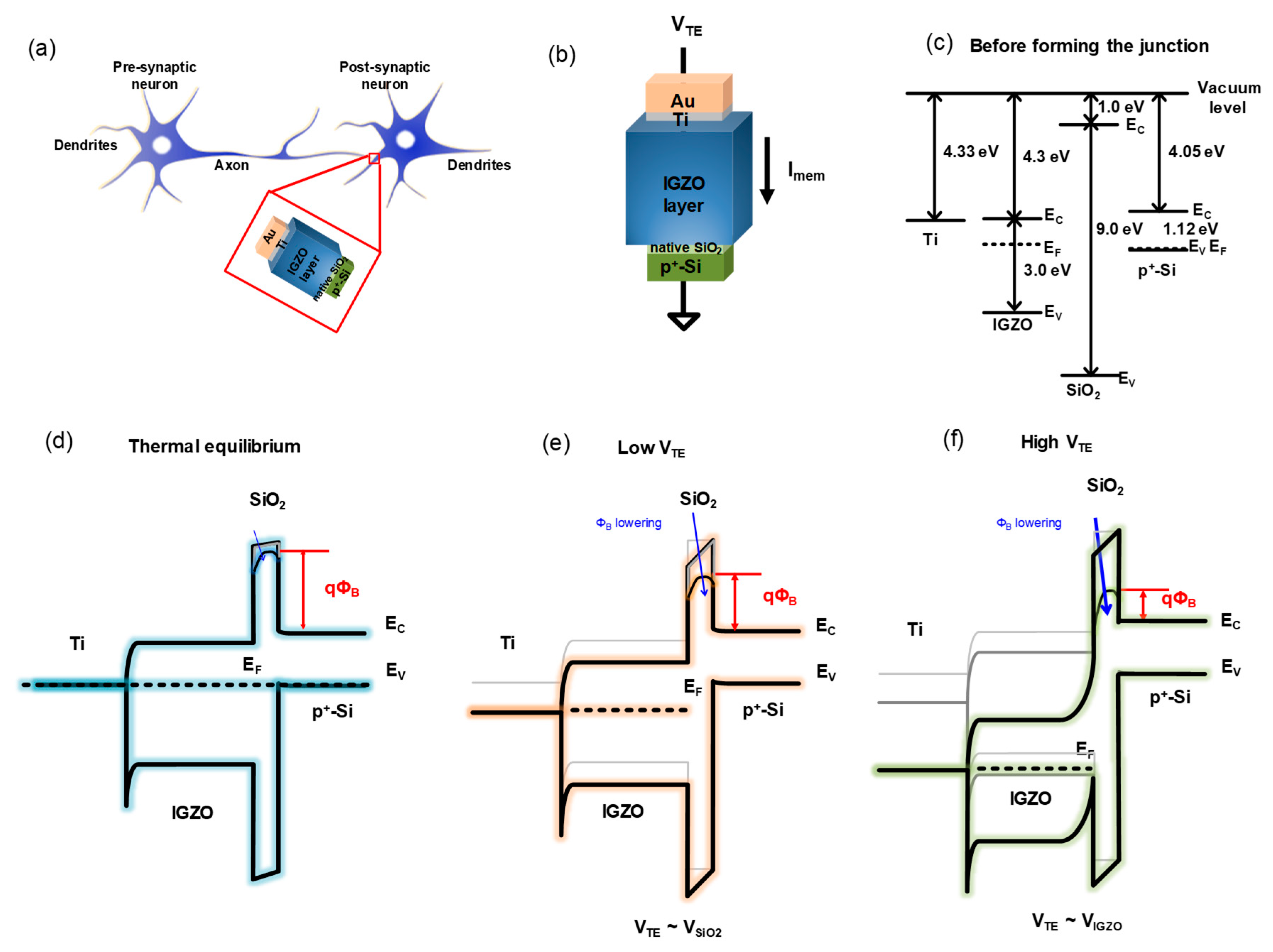
To implement the synapse devices in bio-inspired neuromorphic computing systems (
Figure 1a), we fabricated the two-terminal Au/Ti/IGZO/SiO
2/p
+-Si memristors as shown
Figure 1b. The p
+-Si conductive substrate acts as a global bottom electrode (BE), and the 4-nm-thick SiO
2 was formed on the BE as the tunnel barrier in the interface between p
+-Si and IGZO. Then, the 80-nm-thick a-IGZO film was deposited on SiO
2/p
+-Si using radio frequency sputtering with a power of 150 W at room temperature. We controlled the concentration of oxygen vacancies (V
Os) during the IGZO sputtering by modulating the oxygen flow rates (OFR) to 1.0, 1.15, and 1.3 sccm at a fixed Ar flow rate of 3 sccm and at a constant gas pressure in the sputter chamber of 0.880 Pa. Subsequently, 10-nm-thick Ti was deposited using e-beam evaporation to form an oxygen reservoir layer and act as the top electrode (TE) of the memristor. Finally, the 40-nm-thick Au was deposited using e-beam evaporation to prevent the oxidation of the Ti layer in air.
To analyze the electrical characteristics, the DC current–voltage (
I−
V) characteristics were measured at room temperature and dark conditions using a Keithley-4200 semiconductor characterization system (Tektronix, Seoul, South Korea). In all the measurements, a voltage was applied to the TE, and the BE was always connected to the ground. The TE voltage was symbolized as
VTE, and the current flowing through the IGZO memristor was called
Imem, as shown in
Figure 1b.
Figure 1c–f shows the energy band diagrams under various conditions: before forming the junction (
Figure 1c), at the thermal equilibrium (
Figure 1d), at a low
VTE (
Figure 1e), and at a high
VTE (
Figure 1f). Here, we considered the lowering of the height of the effective SB and denoted it as
qΦ
B (eV). While SB lowering was insignificant at a thermal equilibrium,
qΦ
B became low as the
VTE increased. At a low
VTE, most of the
VTE was applied across the thin SiO
2 layer (
Figure 1e), whereas the increased
VTE was used mainly to deplete the IGZO film (
Figure 1f). Energy band diagrams suggested the fabricated IGZO memristors operated as non-filamentary RS devices based on the SB modulation. The two main concerns were whether the modulated
qΦ
B was nonvolatile and whether its decrease was inversely linear with the increase of
VTE. These two concerns will be discussed later.
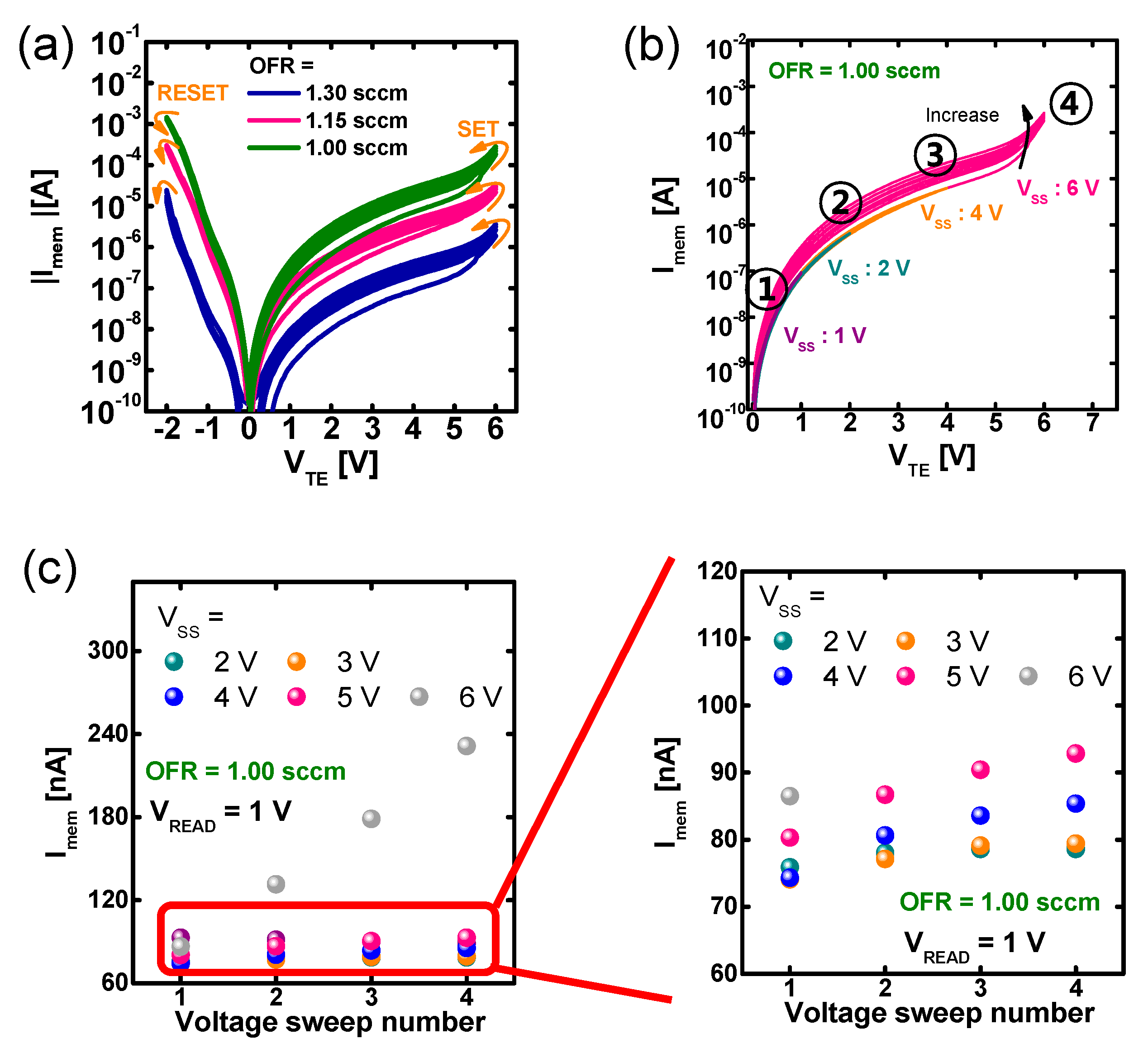
We measured the OFR-dependent
Imem while using a positive
VTE sweep (SET process), that is, 0 V → 6 V → 0 V was repeated four times. Then, a negative
VTE sweep (RESET process), that is, 0 V → −2 V → 0 V was repeated four times, as shown in
Figure 2a. We observed that the current at a fixed
VTE increased as the OFR decreased. This was attributed to the increase of the V
O concentration with the decrease in the OFR because the V
O is a well-known electron donor in the IGZO film [
21,
22]. Along with the SB-modulated non-filamentary RS devices in
Figure 1e,f, a gradual resistance modulation rather than an abrupt RS was clearly observed during repeated
I−
V sweeps (
Figure 2a).
Figure 2b also shows the
Imem−
VTE characteristic of the IGZO memristor with OFR = 1 sccm. In
Figure 2b, the positive
VTE voltage sweep was repeated four consecutive times by changing the stop voltage of the
VTE sweep (
VSS) from 2 to 6 V. When the
VTE sweep was performed four times, the readout current
Imem at
VTE = 1 V increased very slightly for
VSS < 6 V, as seen in
Figure 2c. The continuous and hysteretic increase of current, which is a typical behavior of a memristor, is clearly observed in
Figure 2a,b. There was a significant increase in
Imem only when
VSS ≥ 6 V, which means that the
potentiation threshold voltage between the gradual/abrupt RS (
VPT) was 6 V. Similarly, the
depression threshold voltage was found to be −2 V.
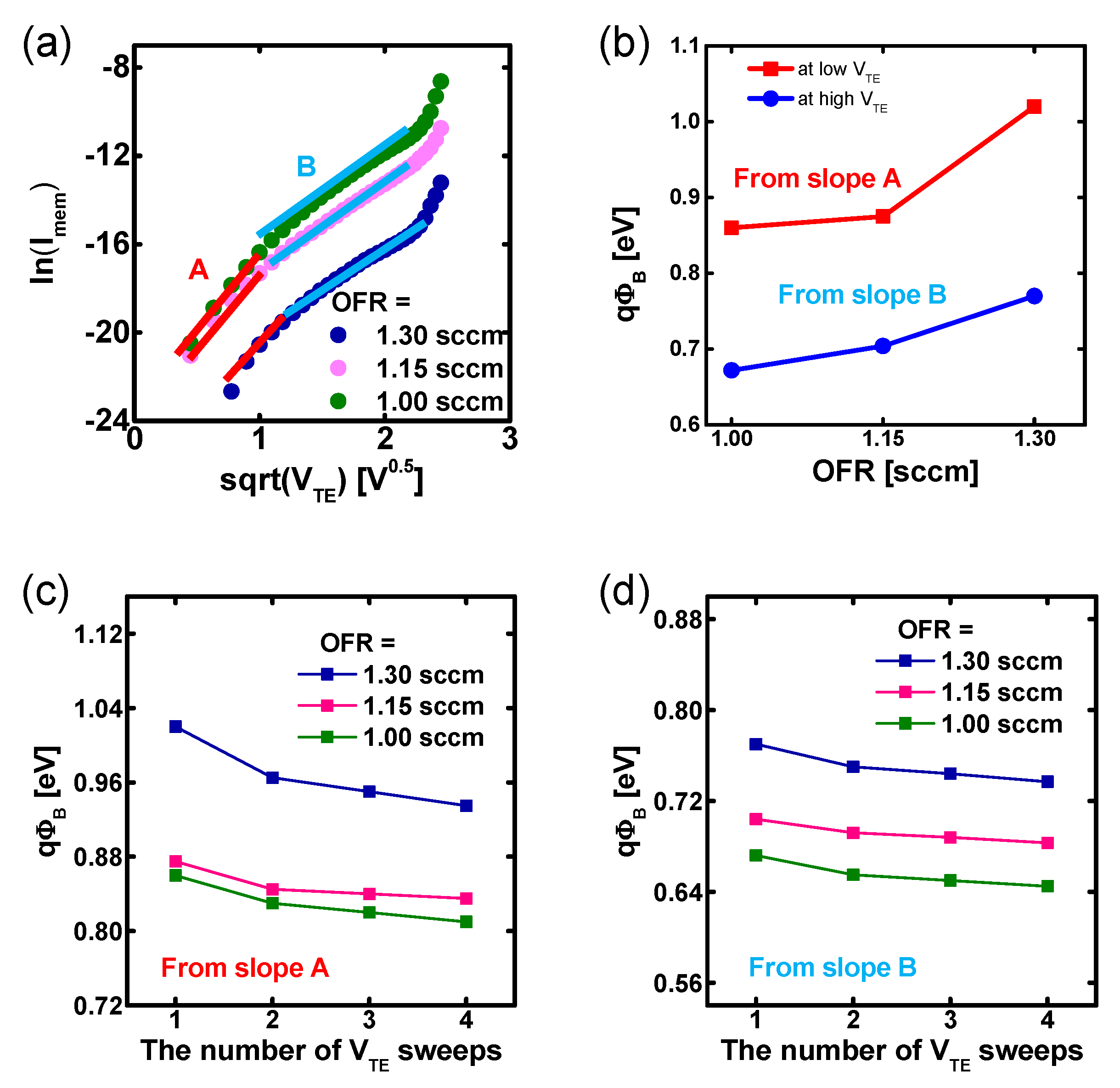
To determine the conduction mechanism, we investigated the relationship between
Imem and
VTE.
Figure 3a shows the OFR-dependent ln(
Imem) versus (
VTE)
1/2 relationships, which were taken from the
I−
V characteristics of the first sweep in
Figure 2a. In
Figure 3a, we observed that the ln(
Imem) was piecewise linear with (
VTE)
1/2, which was strongly reminiscent of the thermionic emission. Noticeably, these linear relationships were clearly classified into two distinguishable values of the slopes A (at a low
VTE) and B (at a high
VTE).
The current due to the thermionic emission through SB is given as:
where
A is the area of device,
A* is the Richardson constant,
T is the absolute temperature,
k is Boltzmann’s constant,
E is the electric field;
q is the electric charge,
ε is the dielectric constant,
XT is the effective thickness of thermionic emission, and Φ
B is the effective SB height. Then, Equation (1) is used for extracting Φ
B. By reformulating from Equation (1) to (2), Φ
B can be extracted by using the y-intercept of the linear relationship between
and
:
Figure 3a,b suggests that at a specific OFR, there existed two Φ
B values taken from the slopes A and B, that is, a large value for a low
VTE (<1 V) and a small value for a high
VTE (1–5 V). Interestingly, we observed this bimodal distribution of Φ
B regardless of the OFR condition and suggest that the SB lowering is nonvolatile and significantly nonlinear with the increase in
VTE. In addition, Φ
B at a specific
VTE was lower because the V
O concentration increases (with decreasing OFR).
However, from
Figure 2a, we can see that the Φ
B modulation depended on the number of positive
VTE sweeps (see
Figure 3c,d). At a specific
VTE and OFR, Φ
B gradually decreased when the number of
VSS sweeps increased.
3. Results and Discussion
In
Figure 3, we can see that Φ
B was modulated by not only the range of the
VTE readout voltage, but also by the number of consecutive
VSS sweeps. Moreover, as shown in
Figure 3b,c, Φ
B depends more strongly on OFR in the slope A case (low
VTE) rather than in the slope B case (high
VTE). Therefore, the results in
Figure 3 provide a clue toward the controllability of the competition between the gradual and abrupt modulations of Φ
B. To understand the mechanism for determining the boundary of an abrupt/gradual RS in IGZO memristor devices, we used
Figure 3 with the energy band diagram.
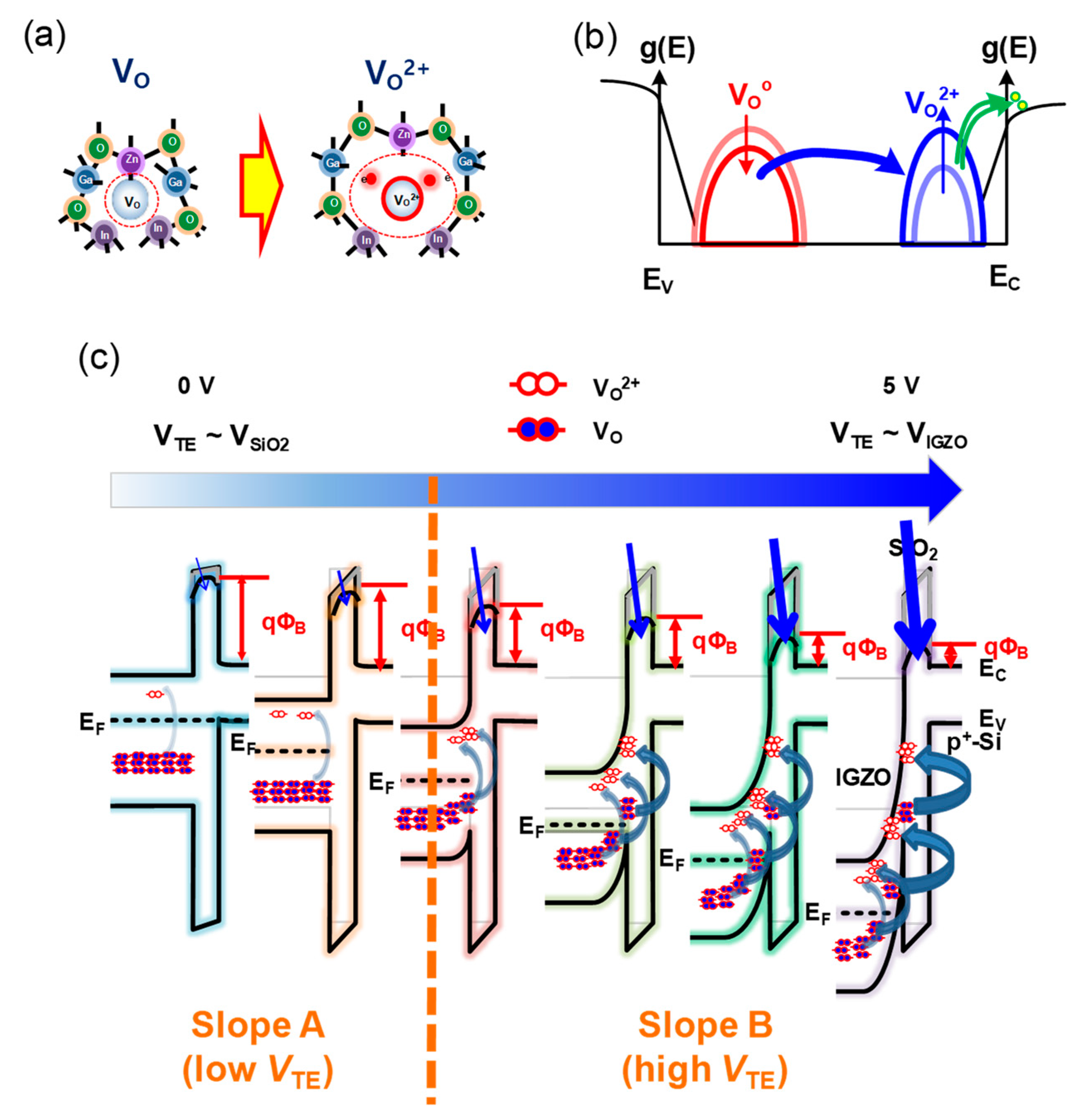
First, when
VTE <
VPT, the bimodal distribution of Φ
B into A and B (
Figure 3a) can be explained as follows. As shown in
Figure 4a, the doubly ionized V
O (V
O2+) is the well-known metastable state [
21,
22] and has been frequently pointed out as having a microscopic origin on the device instability under photo-illumination or bias stress [
22,
23,
24,
25,
26] and persistent photoconductivity [
25,
26]. From the viewpoint of the subgap density of states (DOSs) in the a-IGZO (
Figure 4b), the neutral V
O states (V
O0s) are transformed into V
O (V
O2+s) when the process of V
O0 → V
O2+ + 2e
− becomes energetically favorable. These neutral states are very slowly recovered (nonvolatile) [
23,
24,
25,
26].
In the readout voltage
VTE-dependent energy band diagrams, which are illustrated in
Figure 4c, as
VTE increases, the Fermi-energy level (
EF) in IGZO reduces far from the IGZO conduction band minimum (
EC), and moves closer to the V
O0 states above the IGZO valence band maximum (
EV). It makes the generation of V
O2+s more energetically favorable. When V
O2+s is generated, the concentration of the carrier electrons in
EC increases; the
EF in IGZO again comes closer to
EC. This situation occurs in non-equilibrium; therefore, the generation of V
O2+s effectively makes Φ
B lower.
Thus, if the V
O ionization is nonvolatile, Φ
B would gradually decrease as the readout voltage
VTE increases. In other words, Φ
B has to be inversely linear to
VTE. However, Φ
B was classified into two groups (A and B), as seen in
Figure 3.
Figure 1e,f shows that a large Φ
B (in low
VTE) taken from the slope A corresponded to the voltage range where the maximum
VTE was applied across a thin SiO
2 layer (
Figure 1e), whereas a small Φ
B (in high
VTE) taken from the slope B corresponded to the voltage range where the maximum increase in
VTE was mainly applied across the IGZO film (
Figure 1f). Then, there would be a significant generation of V
O2+s only in the latter range (
Figure 4c). In
Figure 2c,
Imem gradually increased only when
VTE was in the latter range, that is, in the range 2 V ≤
VTE <
VPT. Our discussion indicates that the bimodal distribution of Φ
B in IGZO memristors originated from the generation of metastable V
O2+ states.
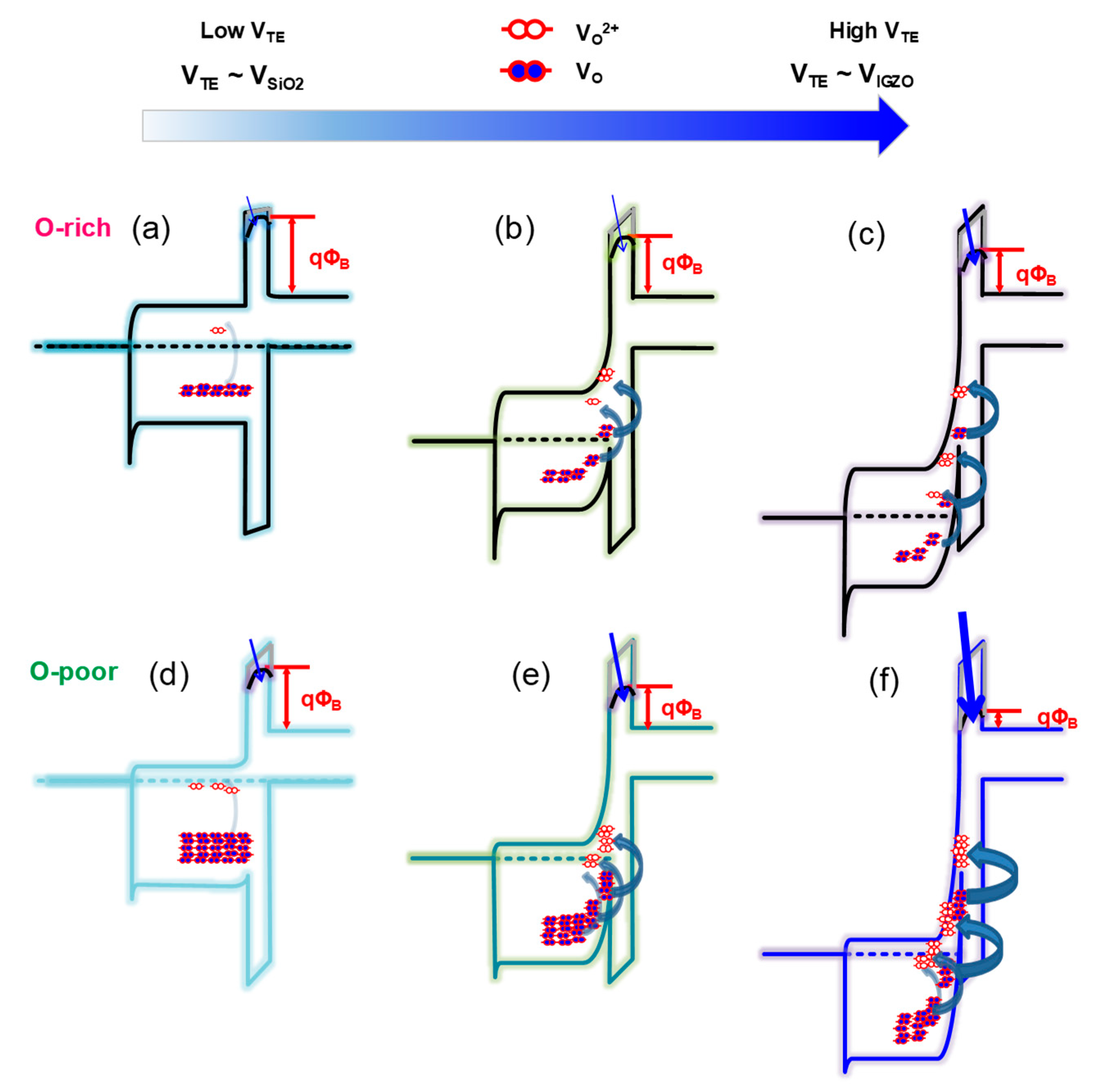
Next, we investigated the OFR-dependence of Φ
B.
Figure 5a–c illustrates the energy band diagram of the device fabricated with a high OFR (O-rich device) under three conditions: at a thermal equilibrium (
Figure 5a), at a low
VTE (
Figure 5b), and at a high
VTE (
Figure 5c).
Figure 5d–f illustrates the energy band diagram of the device fabricated using a low OFR (O-poor device) in three states: at a thermal equilibrium (
Figure 5d), at a low
VTE (
Figure 5e), and at a high
VTE (
Figure 5f). As seen in
Figure 5a,d, a larger amount of V
O0s existed in the IGZO when the OFR decreased from 1.3 to 1.0 sccm. Then, as the IGZO was O-poorer, the IGZO work function decreased, and Φ
B became lower, which is consistent with
Figure 3b. In addition, as mentioned in
Figure 3b,c, the OFR-dependence of Φ
B was larger in the slope A case (low
VTE) rather than in the slope B case (high
VTE). The Φ
B before the V
O2+ generation (at a low
VTE) was determined mainly by the OFR condition. After a significant amount of V
O2+s were generated at a high
VTE, the initial OFR-dependence of Φ
B was combined with the
VTE-dependence of Φ
B. Thus, the OFR-dependence of Φ
B was diluted in the slope B case (high
VTE).
Finally, the evolution of Φ
B with the increase in the number of consecutive positive
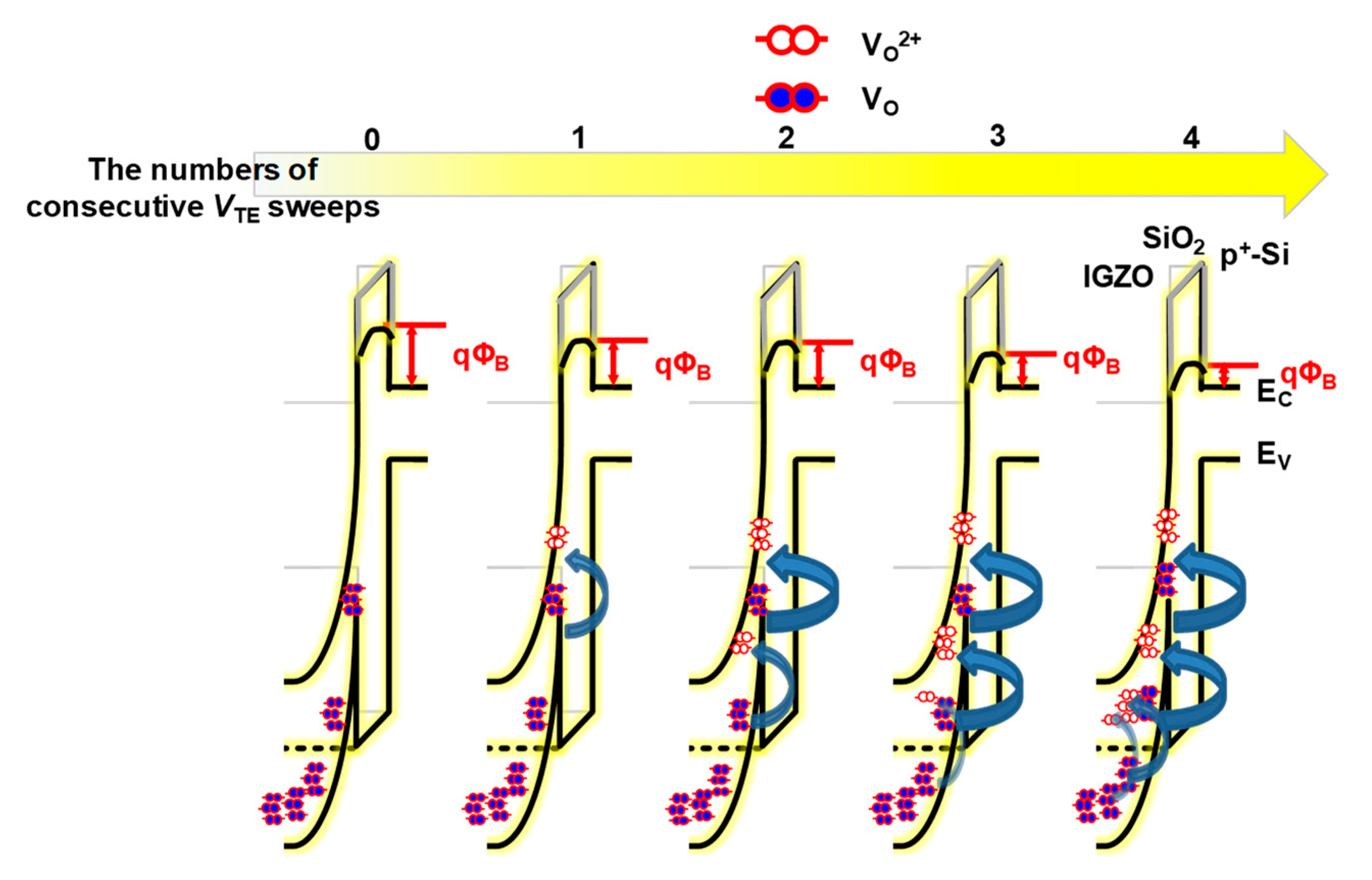
VSS sweeps is illustrated in the energy band diagrams in
Figure 6. When the
VSS sweeps were repeated four times, Φ
B gradually decreased because of the gradual increase in V
O2+s. However, the process of V
O2+ generation followed by Φ
B lowering was not abrupt; it was gradual because further lowering of the
VTE-dependent
EF followed by the V
O2+ generation was self-limited due to the increasing of the electron concentration–dependent
EF. The results in
Figure 3c,d explain this well. If
VTE ≥
VPT, the change of
Imem becomes abrupt because
EF is aligned with the level of the V
O0s peak in DOS (
Figure 4b).
Therefore, we can classify the operation regime in the two-terminal Au/Ti/a-IGZO/SiO2/p+-Si memristors into three parts: (1) low VTE (VTE < 2 V), (2) high VTE (2 V ≤ VTE ≤ VPT), and (3) higher VTE (VTE ≥ VPT). The boundary between (1) and (2) was approximately 2 V in our case; it was determined by the process/structure details and was controllable using the SiO2 thickness and the IGZO work function. The VTE in regime (1) was adequate for the readout voltage because ΦB and Imem were determined mainly by the OFR condition. However, the VTE in regime (2) can be used as the amplitude of the potential pulse because ΦB and Imem gradually change in a nonvolatile manner with the increase in the number of consecutive VSS sweeps. When the VTE in regime (3) was applied to the devices, they operated as abrupt RS switches rather than as gradual RS memristors.

