1. Introduction
A buck converter is a DC–DC power converter that is applied in a wide range of low-voltage technological applications. This converter can be modeled as a piecewise linear system [
1], where the theory and models can be found in ref. [
2]. However, the converter presents significant voltage variations when different types of loads are connected [
3].
A good mathematical model derives from an appropriate balance between simplicity and accuracy. An approach that combines theoretical, simulated, and experimental tests is pertinent to find the best balance. Advances in electronics have allowed the development of rapid control prototyping (RCP) platforms [
4,
5], where real-world systems can be automatically connected with mathematical models [
6]. By integrating theoretical, simulated, and experimental methods, the best model can be identified and its control strategy validated at the same time.
Besides, in ref. [
7], the steady-state limit cycles in PWM-controlled converters were evaluated and, to avoid oscillations, some conditions were imposed on the control law and the quantization resolution. On the other hand, the Fixed-Point Induction Control (FPIC) technique allowed the stabilization of unstable orbits [
8]. Recent control techniques applied to the buck converter are the Zero Average Dynamics (ZAD) and FPIC, which have shown good results for controlling the output voltage [
9].
The internal parameters of an electronic converter may vary depending on the operating conditions. In addition, load variations or the aging of components may occur. Ignorance of these parameters in real time can cause inaccuracies in the design of the controllers [
10], which causes instability throughout the system [
11]. Therefore, adaptive and self-adjusting controllers based on parameter identification are being investigated. Power losses in the circuit must be considered to accurately represent similar results between simulation and experimental tests. In the literature, some authors have focused on estimating power losses in the switching process of the metal– oxide– semiconductor field-effect transistor (MOSFET) [
12]. In addition, the power losses in the core of an inductor in a PWM converter are estimated [
13]. Furthermore, other elements in the circuit produce power losses, such as the capacitor, current sensor, and feeding source, which is why parameter estimation must identify those not considered in the simulation test. The most commonly used methods to estimate the parameters are conventional least squares [
14,
15] and recursive least squares (RLS) [
16,
17]; both techniques help to obtain accurate results when loads are fixed or vary slowly [
10]. Due to the above, the RLS technique is used in this work to estimate these parameters in the circuit.
In ref. [
18], the parameters estimation of a buck converter with digital PWM control and ZAD strategy is presented. A visualization approach was applied in [
19], where the output voltage of a buck power converter is controlled by means of a quasi-sliding scheme. There, the authors introduced the load estimator by means of least mean squares to make the ZAD-FPIC control feasible in load variation conditions, and comparative results for the buck converter with different control strategies (including: Sliding Mode Control (SMC), Proportional–Integral–Derivative (PID) and ZAD-FPIC) were presented.
In ref. [
19], the FPIC technique is used for the control design based on (ZAD) strategy, including load estimation by means of the Least Mean Squares (LMS) method. In ref. [
20], an adaptive ZAD-FPIC strategy is formulated for motor speed control. The system involves a buck power converter, a permanent magnet DC motor (PMDC motor) [
21], and a dSPACE platform; the load torque and the friction torque are considered unknown so that they lead to an uncertain parameter that is estimated by means of a least mean squares (LMS) mechanism, which is formulated and tested on the real system.
A comparative analysis that represents the advantages and drawbacks is presented in
Table 1. This table lists the four applications of ZAD, FPIC, ZAD-FPIC, and ZAD-FPIC with the recursive least squares (RLS) method. ZAD-FPIC with the RLS method has more advantages over the other combinations because it inherits the advantages of the ZAD-FPIC controller and is also robust against changes in the internal parameters of the converter and changes in the load. Therefore, this article shows the development of ZAD-FPIC with the RLS method where parasitic resistance and load resistance are measured.
Additionally, previous works do not estimate losses related to parasitic resistance, which changes due to heating. Besides, neither a description is made of how the experiments were performed and nor is it explained how the sampling and signal synchronization was made with the firing signal given by the Centered Pulse Width Modulation (CPWM) signal. Therefore, this paper presents a detailed method to perform both the experimental test and the synchronization of sampling signals and the effects of parasitic resistance losses, in addition to the real-time controller.
2. Materials and Methods
2.1. Buck Converter Model
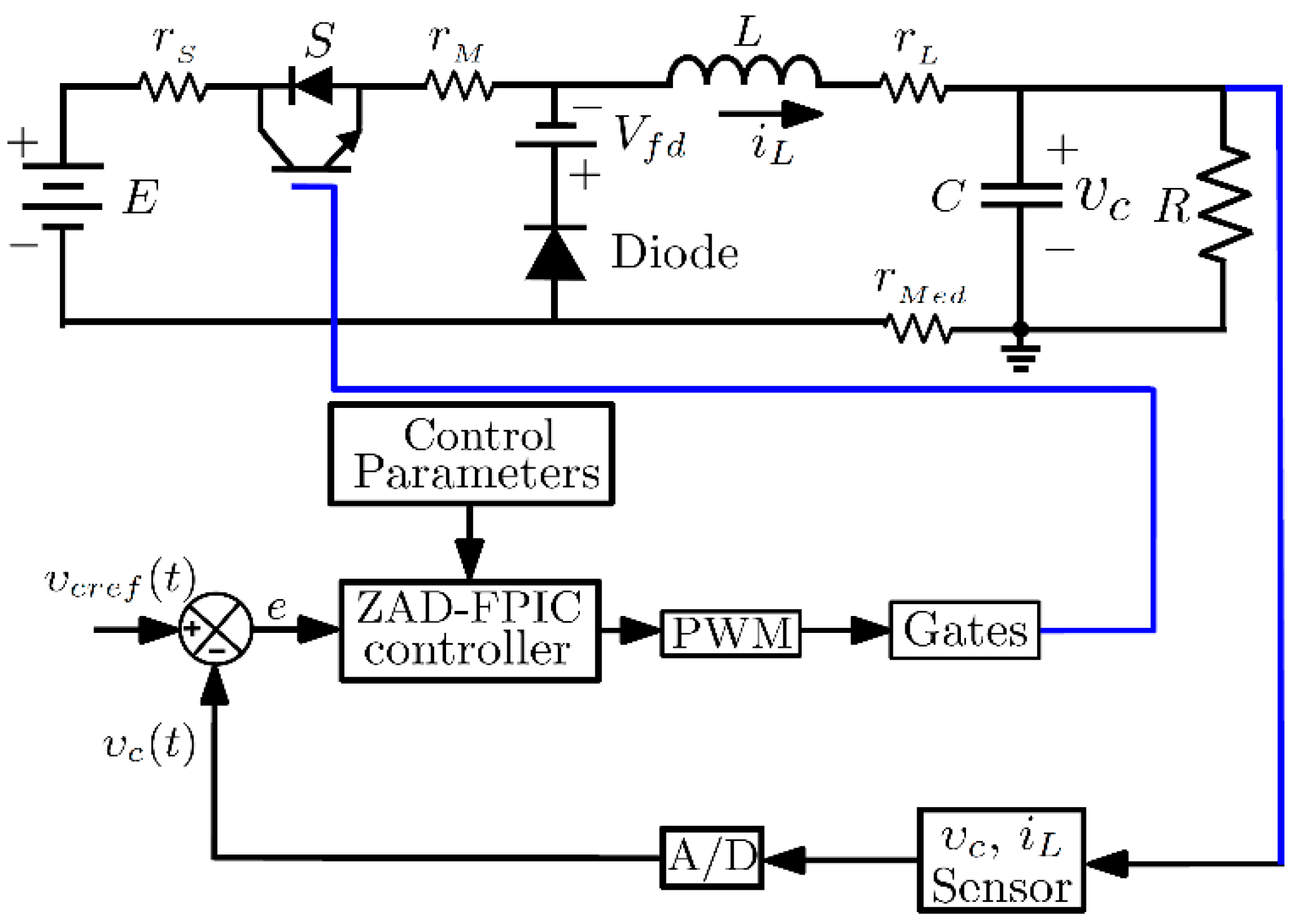
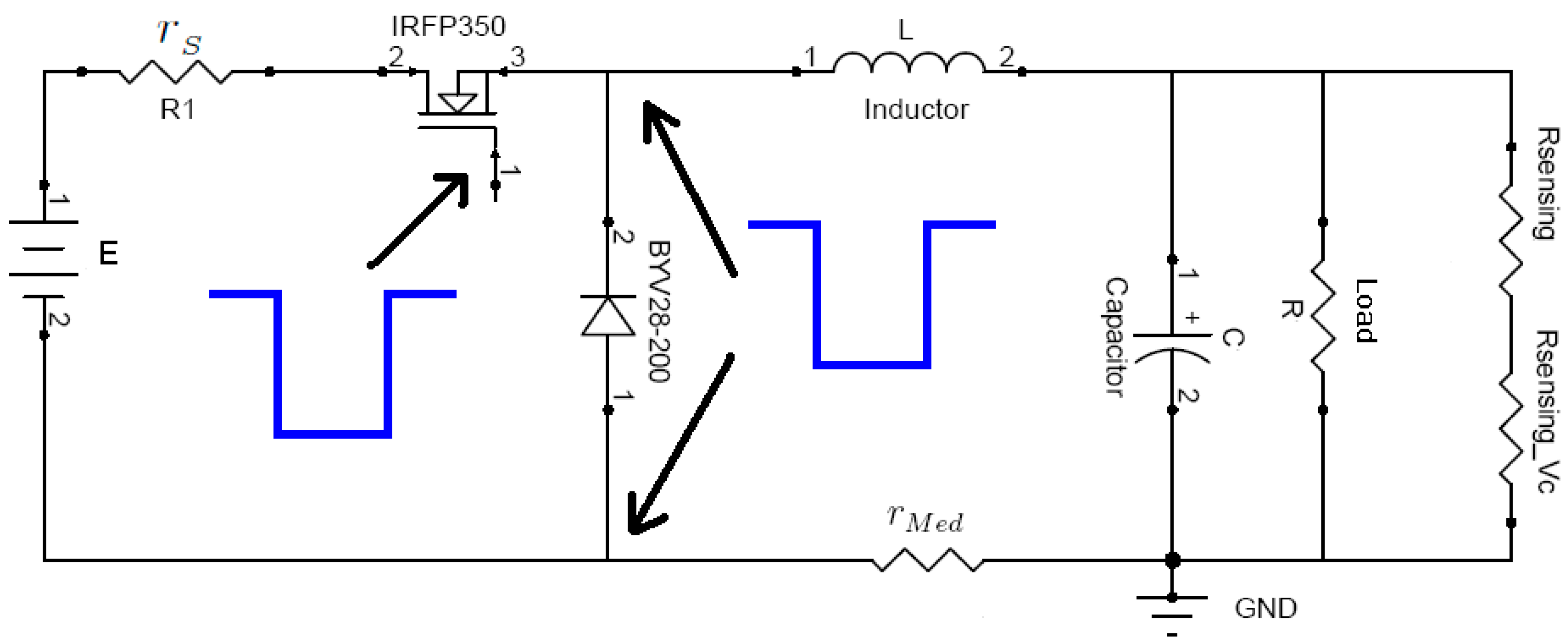
Figure 1 displays a diagram of the buck converter with an integrated control that uses the ZAD and FPIC techniques. The converter has a power source with voltage
, internal source resistor
, an N-Channel MOSFET IRFP350 working as a switch S, an internal MOSFET resistance
, a diode with forward voltage
, a filter
, an internal resistance of the inductor
, a resistance used to measure current
, and a resistance
that represents the load of the circuit.
From the circuit in
Figure 1, the output voltage
and the inductor current
are measured in discrete time at each sampling period
. These measures are the inputs for the ZAD-FPIC control law used to regulate the output signal
. The control requires adjusting the reference voltage
and the control parameters
and
N. These parameters are responsible for the system dynamics and stability regions.
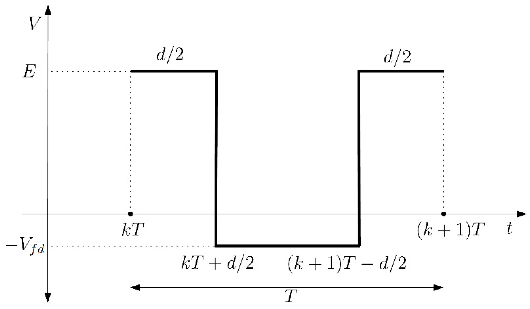
The output signal of the controller enables the CPWM, which drives the change of state in switch S, between ON and OFF, providing the inductor input with a voltage
or
, respectively, as depicted in
Figure 2. This voltage modulator combined with the switch S, the DC power source, and in conjunction with the filter
and the diode D, must supply to the load
an average voltage
during a switching period.
The inductor input signal when using a CPWM gate command is shown in
Figure 2, where the duty cycle
is calculated for each period
, and
is the voltage magnitude. Herein, when the output signal of the CPWM yields the gate command
and the switch S is enabled (state ON), the mathematical model is described by Equation (1):
which can be simplified in the form:
where
,
,
, and
The term
is the capacitor voltage
and
is the inductor current
:
When the output signal of the CPWM indicates the value
, the switch S is disabled (state OFF) and, in this condition, the system can be modeled by Equation (3):
Analogously, Equation (3) can be simplified in the form:
where the terms
,
,
, and
.
Thus, to describe the dynamical system during a complete period
, Equations (2) and (4) can be combined as shown in Equation (5), where
:
The control goal is to ensure the output voltage provided to the load corresponds to a desired reference voltage, namely . The regulation must be performed at each period by computing the proper duty cycle ( ∈ [0, ]), to be applied at the next iteration. Thus, the switch S must be driven according to the CPWM signal, remaining closed for the duration of the duty cycle or when .
2.2. ZAD Control Strategy
The ZAD approach was proposed in ref. [
22] and studied also in refs. [
19,
23,
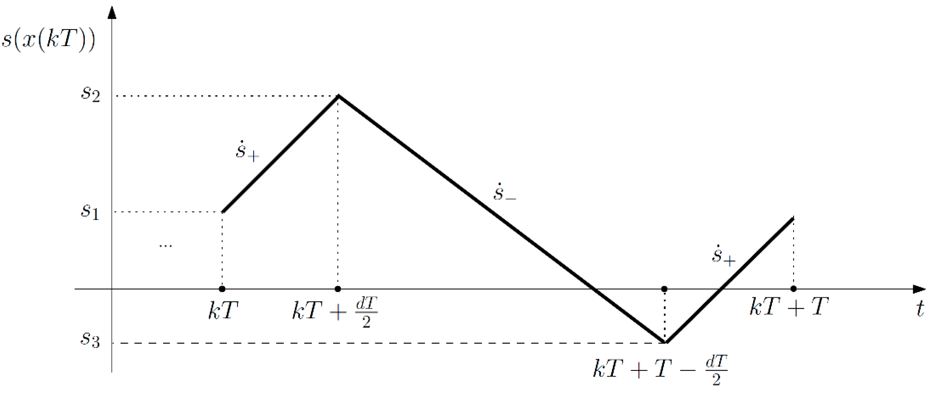
24]. The idea behind the method is to define a sliding error function and force the average error to zero at each sampling period [
23]. Then, suppose that
is the tracking error and
is the sliding surface; thus, it can be represented as a piecewise linear function of the state as given by Equation (6):
where
In this paper,
is assumed to be zero. During a complete sampling period, as shown in
Figure 3, the slopes are calculated from the values of the state variables at the instant of sampling
as shown in Equations (6) and (7). The slopes are then used to compute the duty cycle to be applied in the next control iteration.
In this equation,
, consider that
is a constant of the ZAD. Thus, the mathematical description for the condition of zero average dynamics is given by Equation (8). Herein, the first and third slopes in
Figure 3 have the same values, and to build the piecewise function
it is necessary to obtain information from the state values
and
at instant
Equation (8) is solved to obtain the duty cycle
at each sampling time, which ensures the condition of zero average dynamics when applied to the system through switch S. The duty cycle was obtained in refs. [
8,
22] and can be expressed by Equation (9):
In the experimental test, the state variables are measured to calculate the CPWM with a sampling frequency of 10 kHz and a one-period delay. Thus, the duty cycle used experimentally is given by Equation (10), which means that the actual control law in the current period
is calculated with the values of state variables measured at the previous iteration (
); therefore, instantaneous application is not possible:
2.3. FPIC Technique
This control technique was proposed in ref. [
25], numerically tested in ref. [
26], and experimentally tested in ref. [
8]. Then, the ZAD-FPIC technique applied to the buck converter obtains a new duty cycle expression as shown in Equation (11):
Herein,
is the control parameter of the FPIC, the term
is obtained from (10), and
can be calculated at the beginning of each period as in Equation (12); then, Equation (13) is obtained:
Assuming a duty cycle greater than zero and less than 1, a saturation function given by Equation (14) is applied; therefore, the expression of the duty cycle for the ZAD-FPIC controlled system is as Equation (14). A complete description on the ZAD-FPIC technique can be found in refs. [
26,
27]:
2.4. Parasitic Resistance (or Loss) Estimator
This subsection addresses the problem of parameter uncertainty and proposes a solution to improve the control technique by including a parameters estimation function. In particular, attention is focused on the estimation of parasitic resistances, which are included in the model equations used by the control strategy. In so doing, computation of the duty cycle is improved as well as the control performance.
An online loss estimator is designed and tested in order to have an accurate estimate of losses in the elements of the buck converter. In this case, the RLS estimation method [
28] is used to design the loss estimator. When the switch is ON, the system operates as described in Equation (1) and all losses are estimated from the remaining series circuit. Additionally, the variables must be sensed once the switch is ON and the time is a multiple of
. Thus, the inductor current dynamics is given by:
Let us introduce
as the total resistance parameter. By applying first-order Euler discretization method to Equation (16) at the
-th sampling period, the following discrete expression is obtained:
where
is the digital controller sampling period. Organizing the expression (16), a new equation is obtained as presented in Equation (17), which has been arranged to have the standard form
, which is useful to apply the RLS algorithm [
28]. Here,
is the unknown scalar parameter to be identified, which corresponds to a combined resistance in series:
The recursive algorithm to obtain the estimated
of parameter
is described in Appendix A [
28]. Moreover, applying the first-order Euler integration method, the recursive equation to estimate
is given by:
where the term
is a constant that defines the convergence velocity of the estimator [
28] and
is the initial (nominal) value for estimated parameter. Replacing the terms from Equation (17) into Equation (18), the recursive estimation of parameter
is given by:
with
Implementing the estimator in the Simulink-MATLAB software, the total parasitic resistance was measured and expressed as
in
Figure 4a. Now, the total resistance in the inductor and current measurement is
and the total resistance in the MOSFET and source is
as shown in
Figure 4b.
2.5. Load Estimator
Finally, in order to further improve the performance of the controller, a load estimator is included in the system.
The RLS estimation [
28] method was also used to design the load estimator. From Equation (1), the voltage capacitor equation is given by:
By applying the first-order Euler discretization method to Equation (23) at the
-th sampling period, the following discrete expression is obtained:
which can be written in the form:
Applying the same method as the previous section and considering that the parameter
is the inverse of
, the recursive estimation of the parameter
is given by [
28]:
where the estimated load
is calculated as
and
is a constant similar to in the previous section.
2.6. Hardware Development
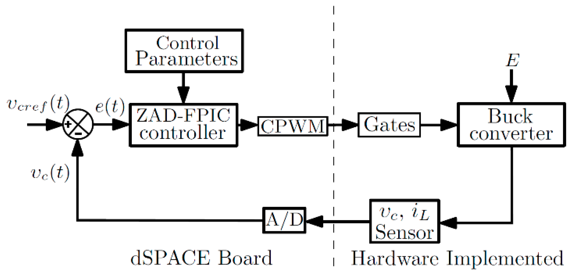
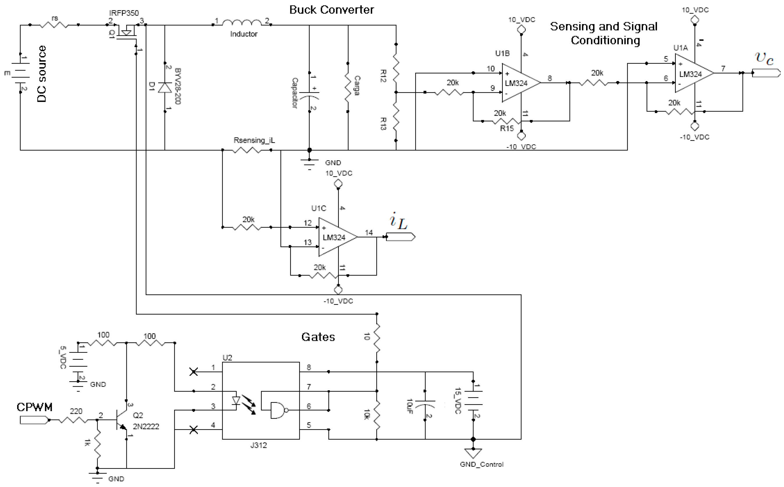
Figure 5 shows the block diagram of the implementation and control of the system with ZAD-FPIC. The blocks on the left side are implemented using dsPACE technology (Paderborn, Germany), in particular, the digital implementation of proposed control strategy is developed in the DS1104 board, while the blocks on the right side include the system hardware. The digital part implemented in the DS1104 board performs the following tasks: acquires signals; converts them from analog to digital; executes the control strategy at each iteration; calculates the duty cycle and generates CPWM signals. The output signal is sent to the opto-coupling circuit, which enables/disables the MOSFET power transistor, to finally feed the Buck Converter. The output signals of the circuit are measured and conditioned by a proper circuit.
Figure 6 shows the hardware implemented to control the converter using the ZAD-FPIC. The implemented triggering circuit is shown to control the ON and OFF states of the IRFP350 MOSFET that acts as a switch for the power converter. This circuit is designed to work up to 100 kHz switching frequencies and the CPWM can be configured. Through the use of an HCP-J312 optocoupler, high-frequency isolation is achieved with good switching and response time characteristics.
2.7. Electric Circuit
The buck converter was implemented with the elements shown in
Figure 7. The power supply is fully regulated and consists of a switched source used for laboratory practices with the possibility of having a variable voltage from 0 to 60 volts with a current up to 6 A. The fact that the power supply used in this work is regulated does not imply that this requirement is met in the actual application. In ref. [
29], it was shown experimentally that when using an unregulated power supply, the regulation error was the same as with a regulated source and this was less than 1% in both cases. This occurred due to the FPIC control that includes the value of the source. The DC source and switch on the left have an internal resistance
= 0.3887 Ω, which was measured in the laboratory by considering full-load and open-circuit tests.
In series with the source a switch is connected that operates to the desired frequency (for this application, 10 kHz). This device is the IRFP350 MOSFET, which has an internal resistance of
= 0.3 Ω taken from the data reported in ref. [
30]. In addition, it has the switching and response time characteristics given in
Table 2, taken from ref. [
30], where it can be seen that it also meets the required specifications.
The diode will conduct when there is a positive current in the coil and the transistor is OFF. This diode (BYV28-200) is of the ultra-fast recovery type (30 ns) and is used in applications of very fast rectification as is the case of switched power sources. The inductor was built in the laboratory and has several advantages. Because it has a ferrite core, it is able to work in the range of a few Hz up to 100 kHz. It has 10 taps, which allows it to obtain 45 values of inductance ranging from 1 mH to 74.21 mH with a current of up to 3 A. The capacitor used is one of the electrolytic type. The load connected is a resistive load and was built in the laboratory; it is composed of 24 resistance of 10
connected two in parallel and then placed in series, in such a way that different resistance values can be obtained with values from 4.863
to 58.641
with the power dissipation shown in
Table 3.
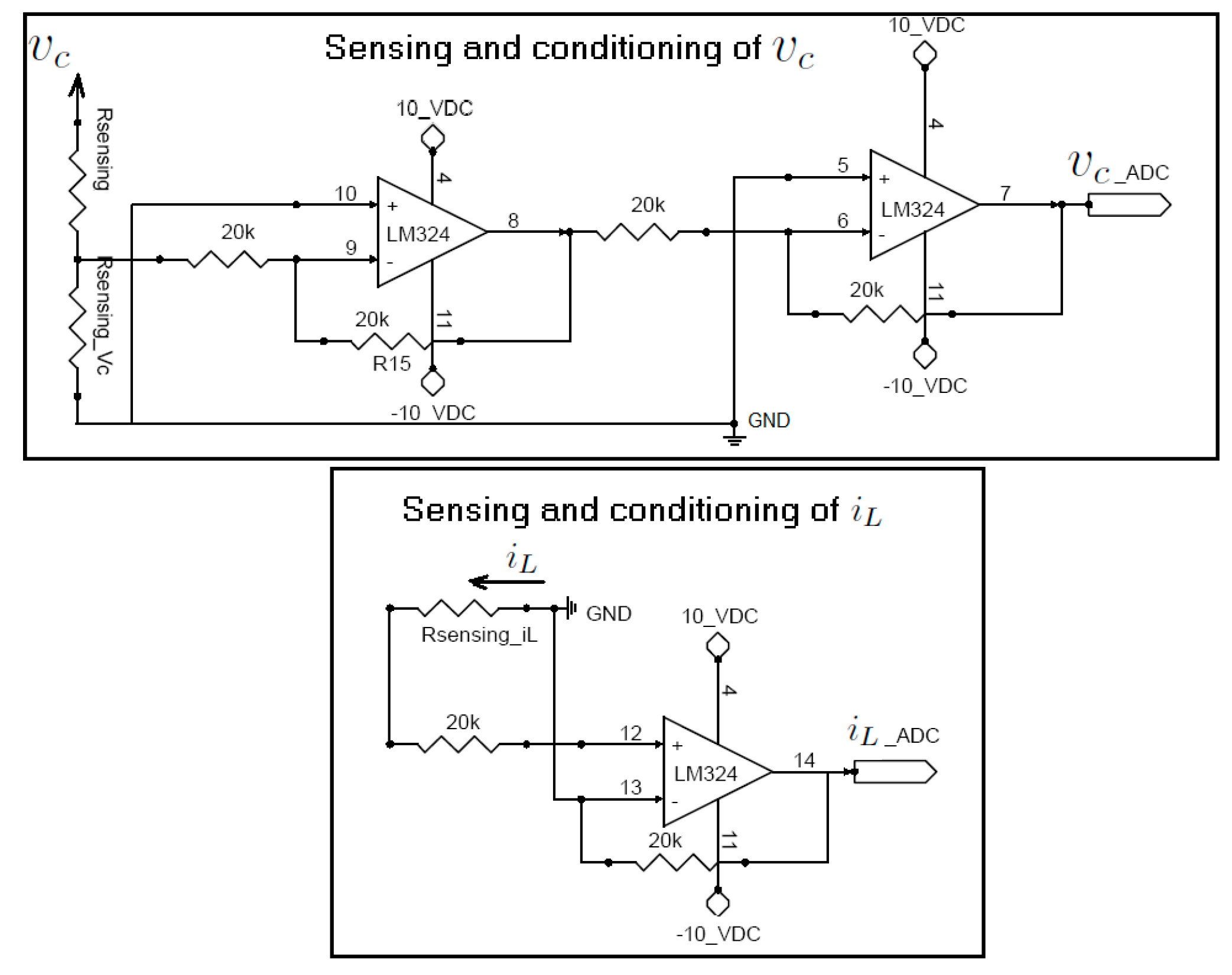
2.8. Sensing and Adequation of Signals
Because there are voltage signals in the load greater than 10 V and the current and voltage signals are disturbed by electromagnetic interferences caused by the switching of the transistor [
31], two circuits were implemented as shown in
Figure 8. Then, the signals were adapted in order to acquire them through the analog-to-digital conversion devices of the DS1104 board (ADC converters).
To sense the voltage, a resistive divider was used in which the voltage signal at the output is attenuated by the gain . The resistors used to sense voltage (Rsensing and Rsensing_Vc) have high values compared with the load resistance to minimally alter the dynamics of the system and are also precision resistances. Because this voltage signal is carried to the DS1104 by one of its analog/digital inputs, it is necessary that the voltage value does not exceed the value of +10 volts because it is the maximum range allowed by the ADC inputs of the DS1104. To ensure that they do not exceed this voltage value, it is necessary to pass the analog signals through a buffer amplifier with operations supplied with ±10 V.
To sense the current, a resistor in series of 1.007 Ω is used from which the value of its voltage drop is taken as the value of the current
. This resistor is composed of four resistors of 10 W in order to avoid heating and errors in the measurements. The signal was adapted as shown in
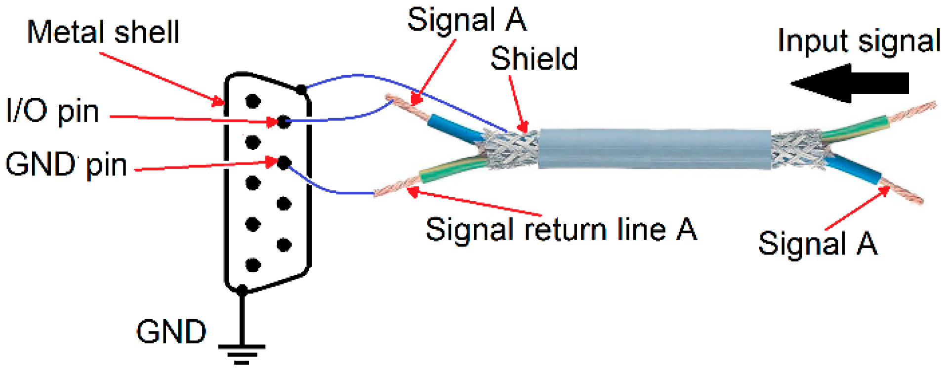
Figure 9 in order to remove the radiated and driven noise present due to commutation [
31]. These voltage and current signals are carried by shielded cable to the ADCHx inputs as shown in
Figure 9, because in practice it was found that by switching the MOSFET there is radiated and conducted noise that adds to the real signals [
31,
32]. For this reason, it was ensured that these signals were fully shielded from the output of the sensors to the inputs of the DS1104 with the configuration shown in
Figure 9.
2.9. Software Development
Simulink is an environment for multi-domain simulation and is designed based on models for dynamic and embedded systems. It provides an interactive graphic environment and a set of block libraries that allows designing, simulating, implementing, and testing a wide variety of linear and non-linear systems in continuous or discrete time or a hybrid of the two, and it even works with different time sampling [
34]. The system under study, which includes the buck converter controlled with the control technique ZAD-FPIC, forms a non-linear system because there are two topologies for each sampling period; it is also a hybrid because it has to work in continuous and discrete time.
The DS1104 board is used to control the system and allow implementation of a rapid control prototype (RCP) because the hardware has a power PC microprocessor with I/O interfaces [
33]. The DS1104 is programmed in the Simulink-MATLAB platform with an interface that captures and visualizes the sensed and processed signals. ControlDesk was the tool used in this work to capture and store signals taken from the physical system.
2.10. Acquisition, Synchronization, and Interruption
For implementation of the ZAD-FPIC control technique, it is necessary to know some values of constant parameters such as
,
,
,
,
,
,
,
,
, and
. In addition, the values of voltage in the capacitor (
) and current in the inductor (
) are also considered for sampling. The values of the parameters are measured from the electrical circuit and placed in the respective inputs of
Figure 10.
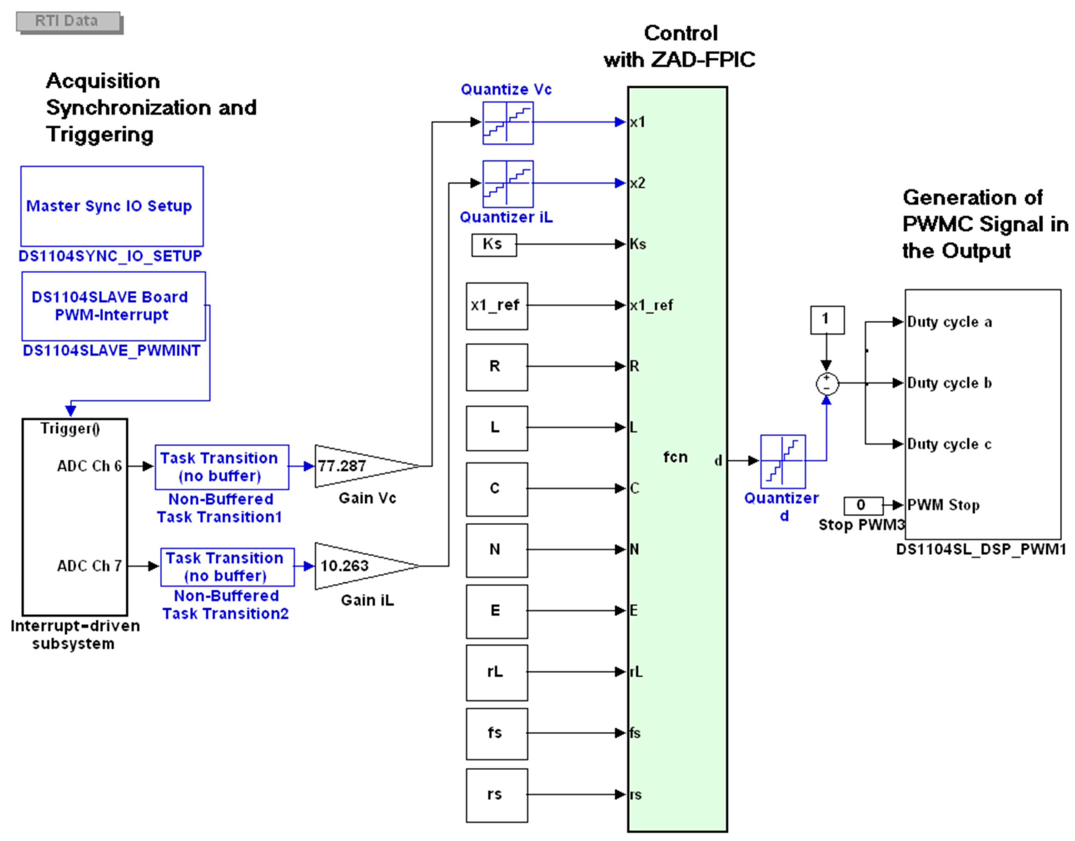
Measurement of the state variables and is carried out by means of a block DS1104 Slave Board PWM-Interrupt whereby an interruption is configured with a trigger signal provided by the Master Sync I/O setup, which is triggered at the beginning of the generation of each signal CPWM. The Master Sync I/O setup block is configured to synchronize the acquisition and processes with the trigger signal. Then, through proportional gains, the and signals are amplified to obtain the correct voltage and current values needed to execute the control technique.
2.11. Control with ZAD-FPIC
Implementation of the ZAD-FPIC control technique was performed using the embedded MATLAB function block from Simulink. The control block is shown in
Figure 10. This block considers the values of the constant parameters and the state variables of the real system, with which the duty cycle defined by the corresponding Equations (11) and (13) is calculated.
In practice, it is necessary to limit the duty cycle () obtained by applying the corresponding Equation (14) so that if the cycle is above 1, then it is necessary to saturate it to 1 and if it is below 0, then it is necessary to adjust it to zero.
2.12. Generation of CPWM in the Output
Using the configuration shown in the right part of
Figure 10, the same duty cycle is entered into the three inputs of the CPWM generation block in order to have only one CPWM output and its inverted CPWM signal (CPWMinv). The outputs CPWM and CPWMinv have the following characteristics among many others: they are complementary, centered, of constant switching frequency in the range of 1.25 Hz to 5 MHz, they are signals of the TTL type, they are protected by a dead time (deadband), and their initiation mode and its stop time are controllable.
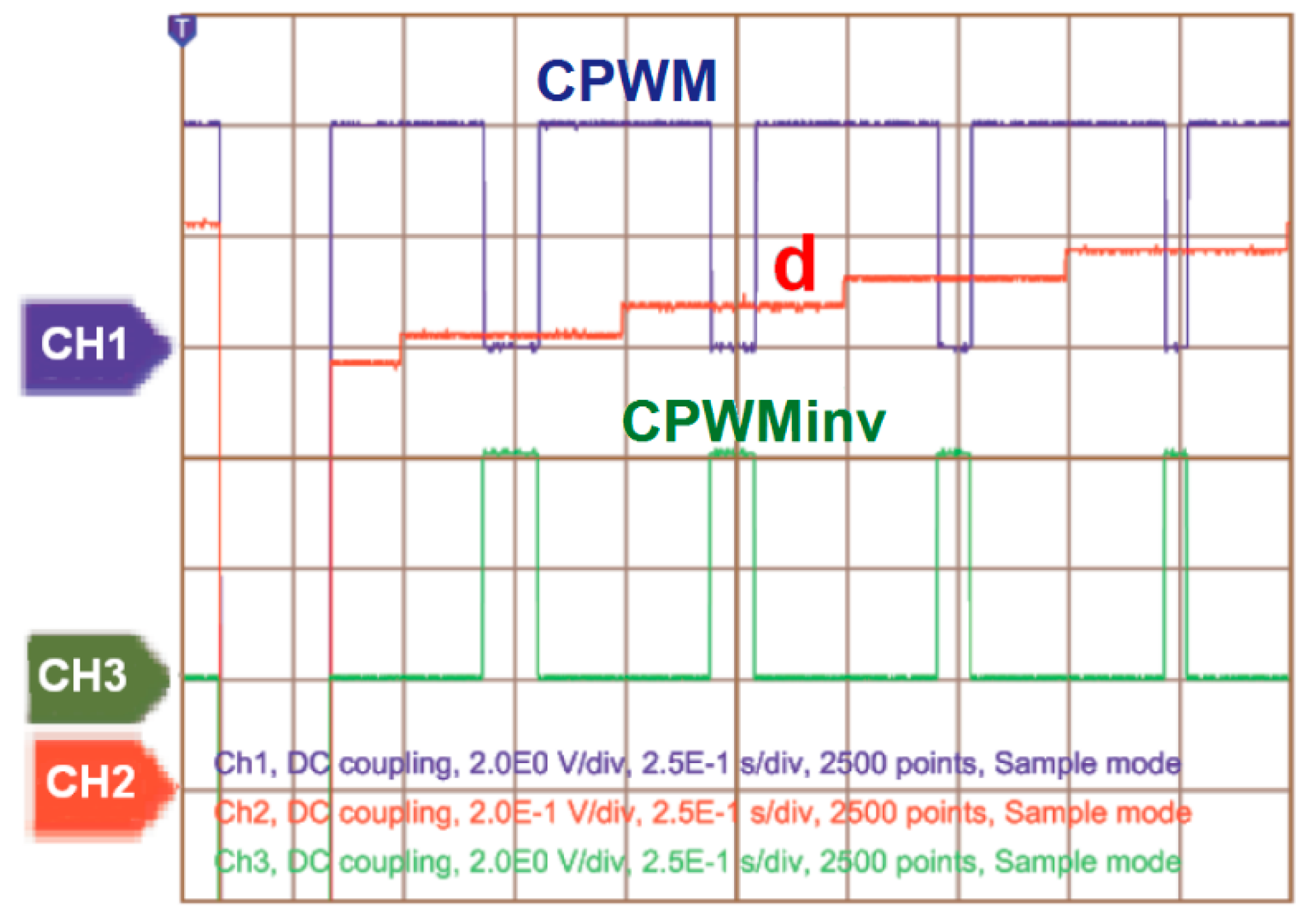
Figure 11 shows that CH1 is the CPWM output, CH3 is the CPWMinv, and CH2 corresponds to the duty cycle
and changes proportionally with time.
When performing sampling synchronization via the ADC channels with a trigger signal obtained from the digital PWM output, a one-delay period (1Tp) is presented. This phenomenon is illustrated in
Figure 12, which shows the following signals: the signal generated CPWM in blue (CH1); the duty cycle (green signal), which corresponds to a sawtooth signal produced by a signal generator; and the signal (sampled) (CH4) that corresponds to the duty cycle sampled at a frequency given by the trigger signal (CH2) for, in this case, 10 kHz.
Thus,
Figure 12 shows clearly that when sampling an external signal (Generator Input) at a given switching frequency, and with it generating the CPWM pulse train, a full delay period is presented (1Tp). Therefore, in the rest of the document, all results, both numerical and experimental, are made, taking into account that the time required to sense a signal and then execute the control action is equal to one sampling period (1Tp). This means that there is a delay period equal to the inverse of the switching frequency in all signals sensed at the input. The main consequence of having a delay period is the presence of chaos and instability in the controlled system with only the ZAD control technique, which was demonstrated in refs. [
29,
35]. Therefore, chaos and instability are controlled with the FPIC control technique [
35]. That is why in the rest of the document the system is controlled with the ZAD-FPIC control technique.
3. Results
Table 4 shows the parameters obtained with an exact measurement to perform the simulation and experimental tests according to the losses and load estimations performed in
Section 2.4 and
Section 2.5.
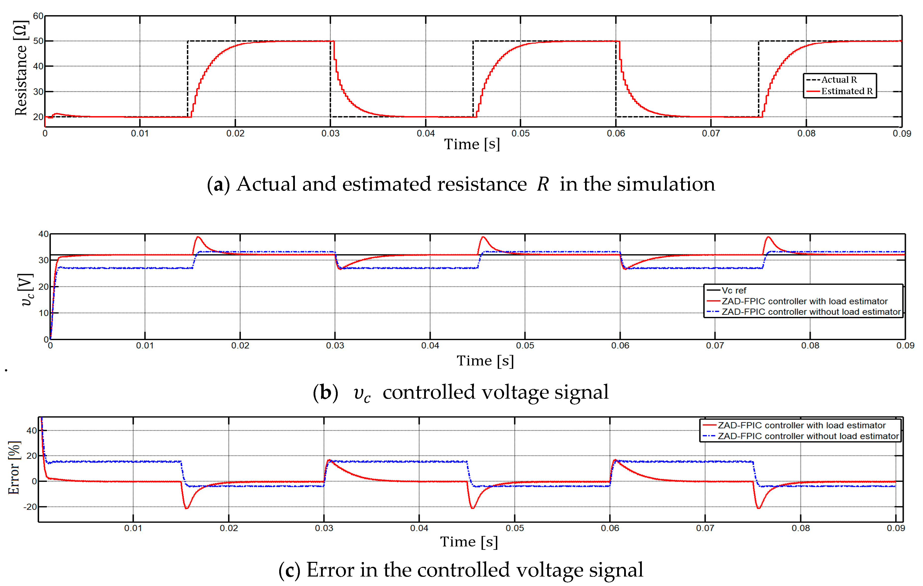
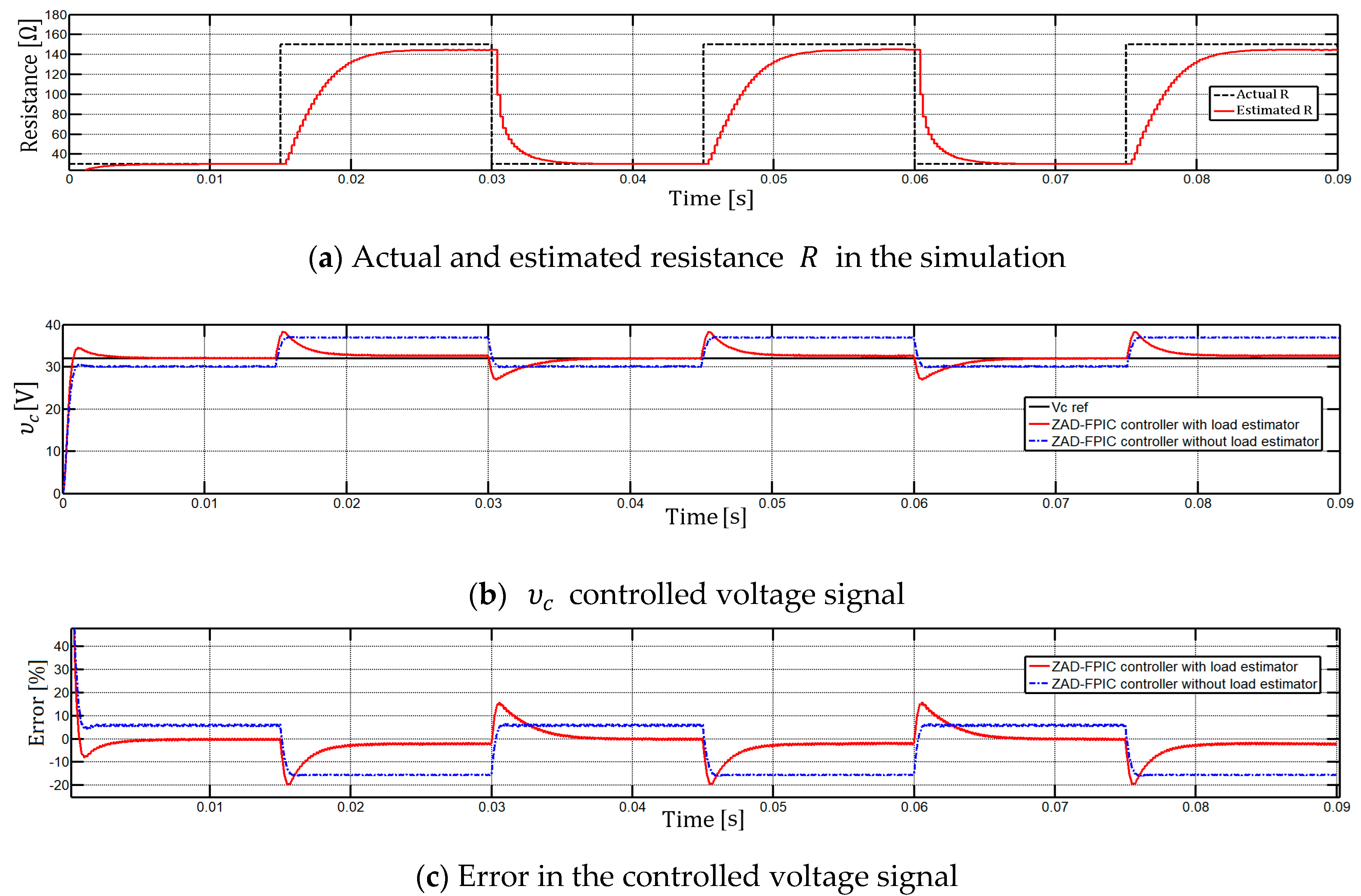
To show the advantages of the ZAD-FPIC with the RLS method over the conventional ZAD-FPIC, the behaviors of the two controllers are presented with variations in the load.
Figure 13 and
Figure 14 illustrate the simulation for cases of the circuit with and without the estimator when the load varies from
to
and from
to
. From
Figure 13a and
Figure 14a, it can be seen that the controlled variable
for the ZAD-FPIC controller without the load estimator has a greater overshoot and a longer establishing time than the controller without the load estimator because the RLS method has a delay time for high-speed changes signals.
Table 5 shows the steady-state error for the controlled voltage
for both ZAD-FPIC with and without load estimator. From
Figure 13a and
Figure 14a, it is concluded that when the load estimator
is used, the system presents less steady-state error for the different values of the load resistance. When ZAD-FPIC with load estimator is used, it is observed that the error increases directly with the increase in the load resistance. This is because the estimated resistance for large values of
does not reach the current resistance value. When ZAD-FPIC without load estimator is used, it is observed that the error tends to be greater at lower and higher resistance values because the controller parameters required a constant resistance value of 40
; therefore, for values close to 40
, the error tends to be smaller.
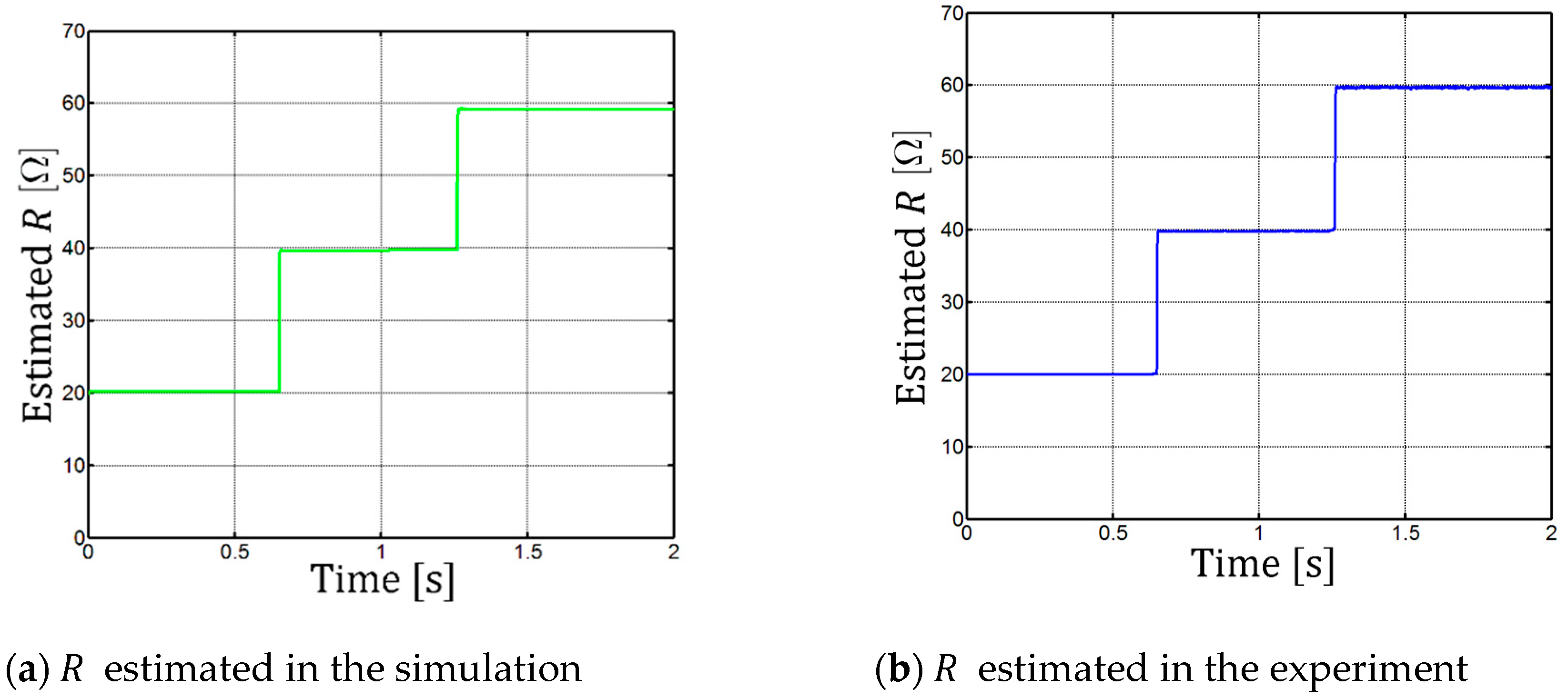
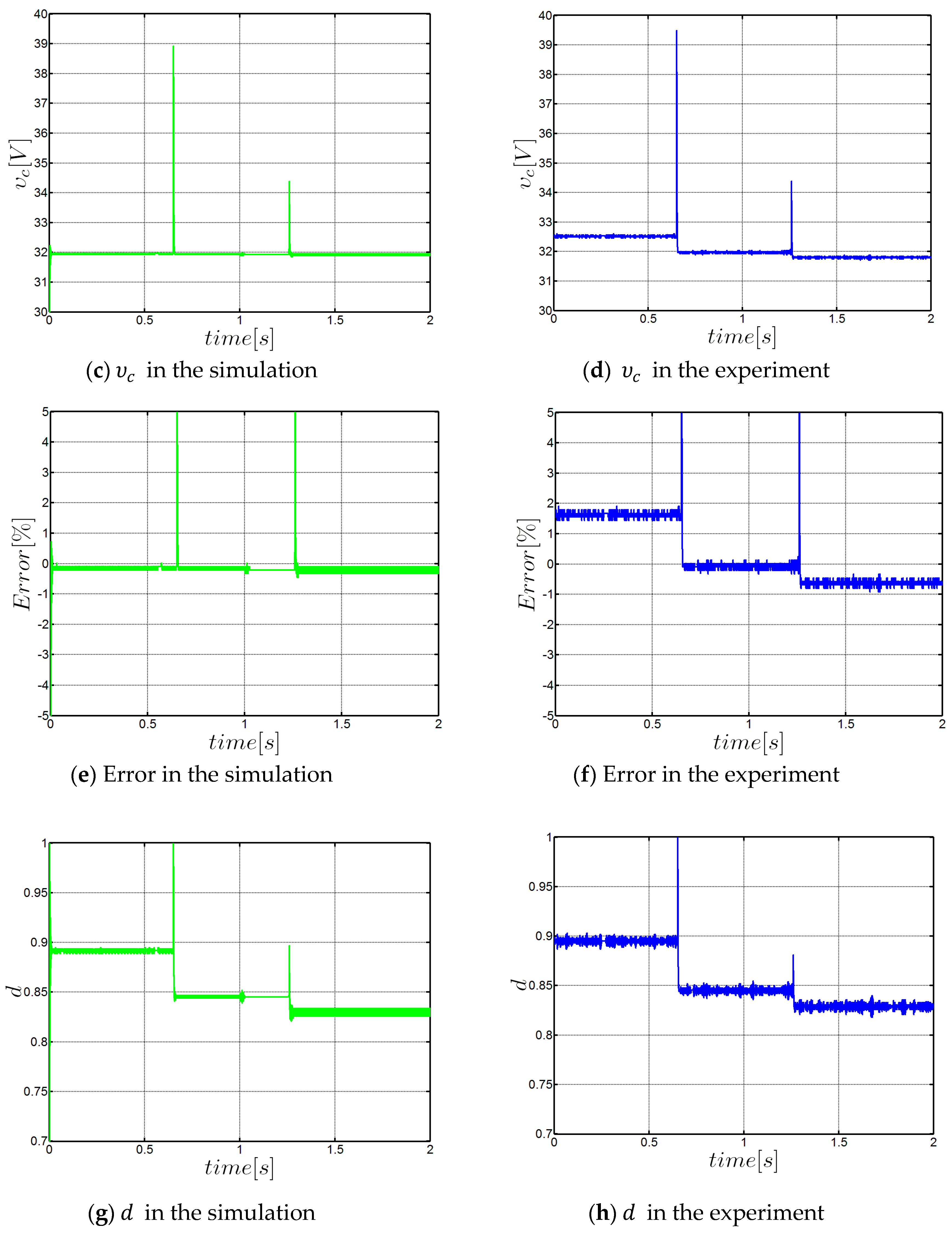
To validate the performance of the parameter estimation approach with simulation and experimental tests, instantaneous load changes are made in order to test the estimator of
.
Table 6 shows the times and the load connected to the converter to test the estimator with
= 1. The parameters of the converter and controller are shown in
Table 4 and the control parameters are fixed as
= 1 and
= 5. The switching and sampling frequencies are assigned at 10 kHz. The results are shown in
Figure 15 and
Figure 16.
Figure 15e,f show that the ZAD-FPIC controller regulates the output voltage
well, with errors below 2%. Regarding the duty cycle in both the numerical and experimental tests (
Figure 15g,h, respectively), it can be seen that it is not saturated; therefore, the system has fixed computation frequency in both cases.
Table 7 shows the numerical and experimental errors when using the ZAD-FPIC controller without load estimator. From the experimental results it is observed that for smaller values of the load resistance, the error tends to increase because there are losses in the experimental circuit and these still need to be estimated.
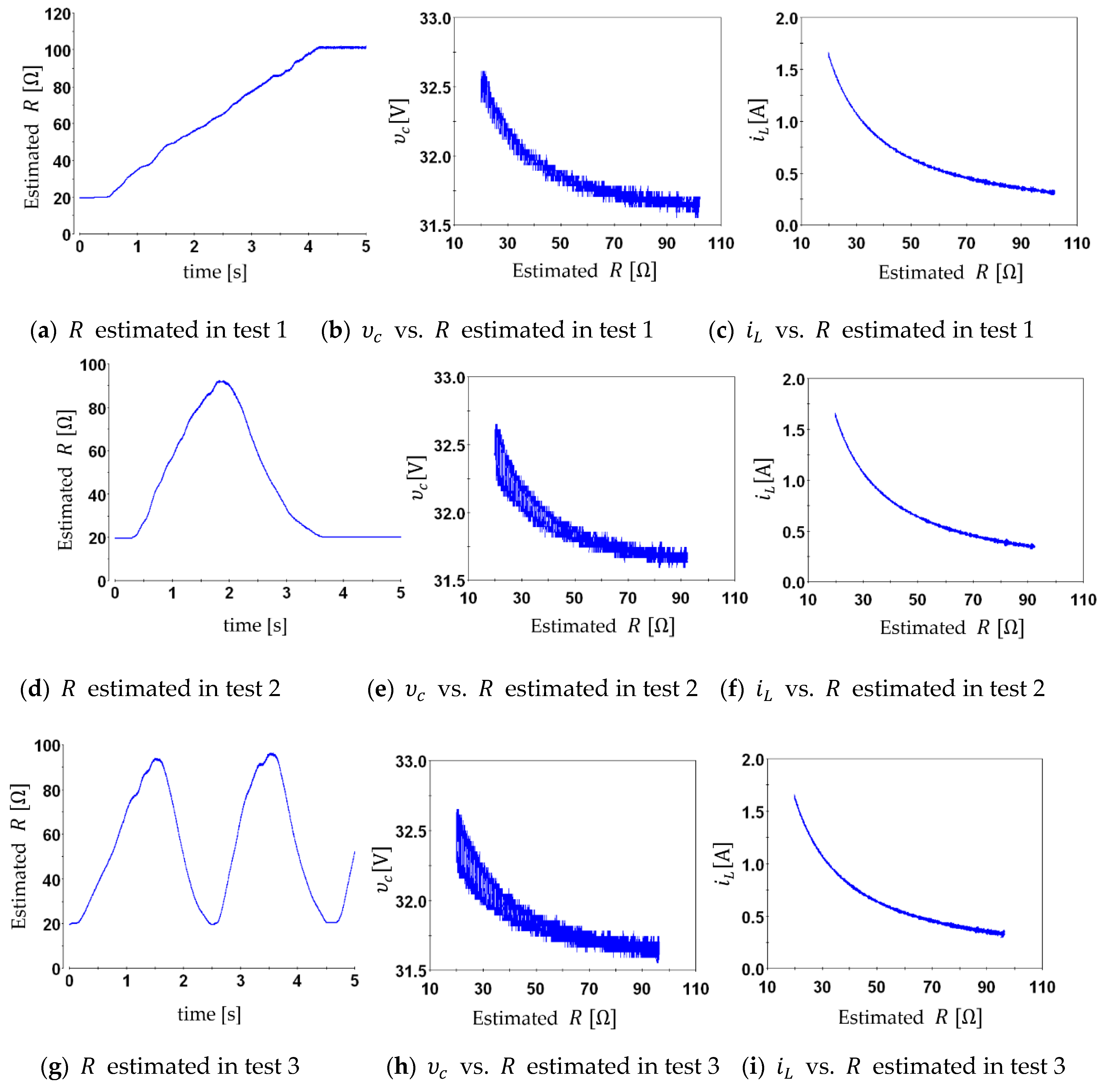
Figure 16 shows the behavior of the system when irregular changes in the load are presented. After large changes in the load, the output voltage remains close to the reference value
V. It is observed that the system is stable to changes in the load. The voltage
remains fixed while the current
varies considerably and, in all cases, the error is less than 2%. Finally, in
Figure 16g,h, it is observed that for the positive and negative growth of the load resistance the system regulates the controlled signal
well and presents low steady-state error.
4. Conclusions
This paper presented the development of a buck converter controlled with a quasi-sliding mode control combined with a loss estimator function to compensate internal losses in the buck converter. Detailed electric and electronic circuits were presented that describe the triggering of the power transistor (N-Channel MOSFET IRFP350) and shielding of wires for reduction of electromagnetic interference to measure voltage and current signals in the capacitor and inductor, respectively. The digital controller is implemented in real time using dSPACE technology (DS1104 board) to manage properly the digital and analogic signals that drive the power system. A detailed description was presented to build the PWM signal with pulse at the center and to ensure proper synchronization in the real-time implementation. In so doing, signals from the buck converter are sampled at each period of time, avoiding measurement uncertainties when sampling on the Poincarè surface. Experimental results showed the effectiveness of the experimental implementation and, of course, the good performance of the model-based control law with loss estimator function to compensate internal losses in the buck converter.
The same control methodology presented in this paper can be applied to other power converters such as the boost and buck boost. For both cases, it is necessary to write the mathematical models to compute the duty cycle. Additionally, for both cases, a suitable regression method can be identified to estimate the unknown parameters and implement them in real-time to obtain the parameters separately, which will avoid problems with estimator convergence. It was verified numerically that the RLS method does not measure parameters that present high-speed changes. Additionally, it was observed that for lower load resistance, values of the steady-state error increase because it is possible to have parameters in the circuit that still have not been modeled. In the experimental results, it was observed that for smaller values of the load resistance, the error tends to increase because some power losses still require to be estimated.


