
Article

An Optoelectronic CMOS Transimpedance Amplifier Using an FVF-Based Low-Dropout Regulator for PSRR Enhancement


Division of Electronic and Semiconductor Engineering, Ewha Womans University, Seoul 03760, Republic of Korea
*
Author to whom correspondence should be addressed.
These authors contributed equally to this work.
Electronics 2026, 15(9), 1771; https://doi.org/10.3390/electronics15091771
Submission received: 1 April 2026 / Revised: 19 April 2026 / Accepted: 20 April 2026 / Published: 22 April 2026

Abstract

This paper presents a flipped-voltage-follower low-dropout regulator (FVF-LDO) for power supply rejection enhancement and low-power operation in CMOS transimpedance amplifiers for optical receiver applications. The proposed FVF-LDO ensures high stability and reliable regulation over a wide range of load conditions by employing a flipped-voltage follower for fast local feedback and improved power supply rejection, while a super-source follower enhances the transient response through increased current-driving capability. A bandgap reference with a 3-bit trimming DAC is adopted to compensate process variations and support stable LDO operations, achieving a temperature coefficient of 19.6 ppm/°C over a wide range of −25 °C to 125 °C. The FVF-LDO exhibits a 101 mV undershoot under a 100 µA-to-10 mA load step with a 100 ns edge time. When applied to an optoelectronic inverter-based active-feedback transimpedance amplifier (TIA), the regulated supply improves the power supply rejection ratio (PSRR) from −6 dB to −38.3 dB. The proposed optoelectronic TIA realized in a 180 nm CMOS process achieves 67 dBΩ transimpedance gain, 869 MHz bandwidth, 66 dB dynamic range, 6.68 pA/√Hz input-referred noise current spectral density, and 4.68 mW power consumption from a single 1.8 V supply. The proposed TIA chip occupies a core area of 940 × 162 µm2.

1. Introduction

State-of-the-art optical receiver systems for short-range sensing and communication applications have attracted significant attention due to their growing usage in areas such as indoor mapping and navigation, LiDAR monitoring, and energy-efficient interconnects. These applications mandate compact and fully integrated circuit solutions that achieve low power consumption while maintaining reliable signal processing performance. In such systems, power supply noise has emerged as a critical bottleneck, particularly in low-voltage implementations where supply fluctuations directly degrade analog front-end performance.
In a typical optical receiver, incident optical signals are converted into electrical currents by a photodetector and subsequently processed by a transimpedance amplifier (TIA) that is followed by post-amplification and digital processing stages. Among these building blocks, the TIA plays a critical role in determining the overall system performance, as it directly amplifies weak input currents and sets the noise and bandwidth characteristics of the optical receivers [1,2,3].
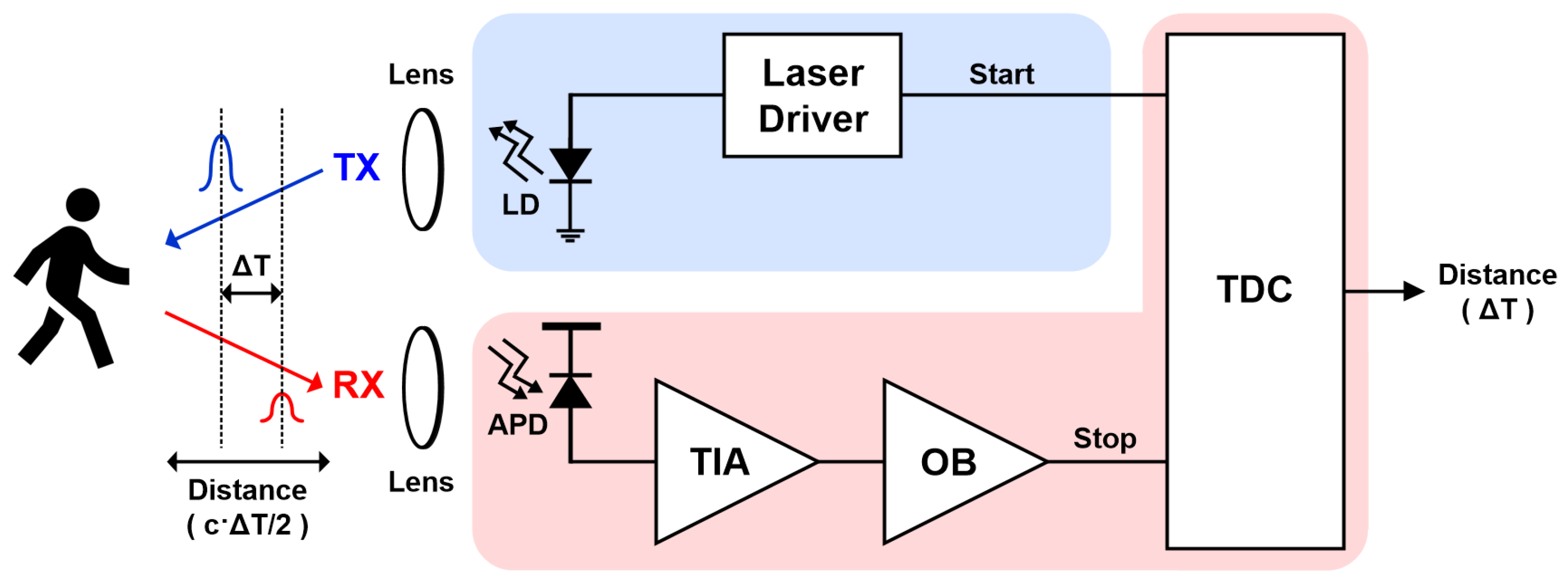
As an example, Figure 1 shows the block diagram of a light detection and ranging (LiDAR) sensor system that equips a TIA as the front-end circuit, demanding low-noise and low-power characteristics.
Particularly for the purpose of low-power operations, the inverter-based TIA architecture has been widely adopted due to its high transconductance efficiency [4]. However, unlike conventional current-biased designs, inverter-based TIAs inherently rely on the supply voltage to establish their operating point. Therefore, key parameters such as transconductance, gain, and output common-mode level are strongly dependent on the supply voltage. Consequently, supply noise directly modulates the operating point and effective transconductance of the amplifier, leading to output signal alterations and degradation in gain stability, linearity, and input-referred noise. This issue becomes more critical under low-voltage operations, where limited voltage headroom further signifies the impact of supply variations.
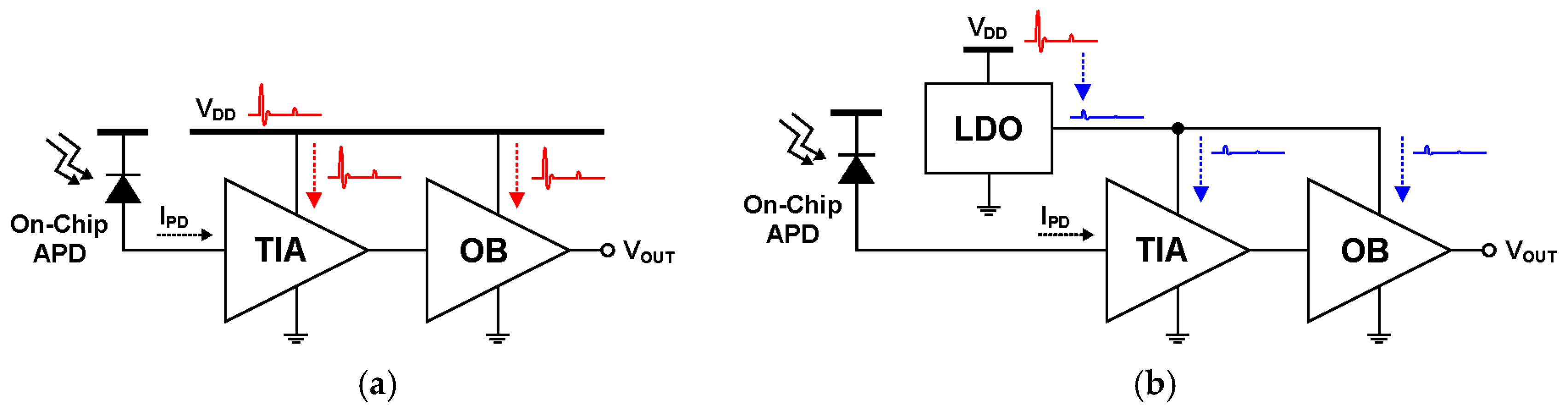
Figure 2 illustrates the effect of power supply noise on inverter-based TIAs, comparing cases without and with supply regulation. In Figure 2a (without LDO), supply noise is directly coupled to the TIA, resulting in output signal variations and degraded performance. This direct coupling yields poor power supply rejection ratio (PSRR), as supply fluctuations are readily transferred to the output.
In contrast, Figure 2b shows the case with supply regulation, where an LDO is employed to suppress supply noise before it reaches the TIA. Conventional approaches typically use off-chip LDOs with large output capacitors to improve PSRR and stabilize circuit operations. However, such solutions are not well suited for fully integrated systems due to their reliance on bulky external components, increased system complexity, and limited scalability [5]. More importantly, these approaches typically treat the TIA and power regulation as independent blocks, without explicitly addressing the intrinsic coupling between supply noise and the TIA operating point. Hence, supply-induced variations are not effectively suppressed at the circuit level, particularly in inverter-based architectures where the operating point is highly sensitive to supply fluctuations.
To alleviate these challenging issues, this paper presents a co-designed TIA-LDO architecture, i.e., an on-chip LDO based on flipped-voltage follower (FVF), which provides low output impedance and fast transient response while enabling full integration without large external capacitors [6]. To ensure stable operations across a wide range of load conditions, a super-source follower (SSF) is incorporated to enhance the loop stability [7]. In addition, a bandgap reference (BGR) is employed to provide a stable and supply-independent voltage reference because the regulation accuracy of LDOs is fundamentally determined by the stability and precision of their reference voltage [8]. However, practical BGR implementations exhibit deviations due to the notorious process variation and device mismatch, which consequently degrades the overall regulation accuracy under process, voltage, and temperature (PVT) conditions.
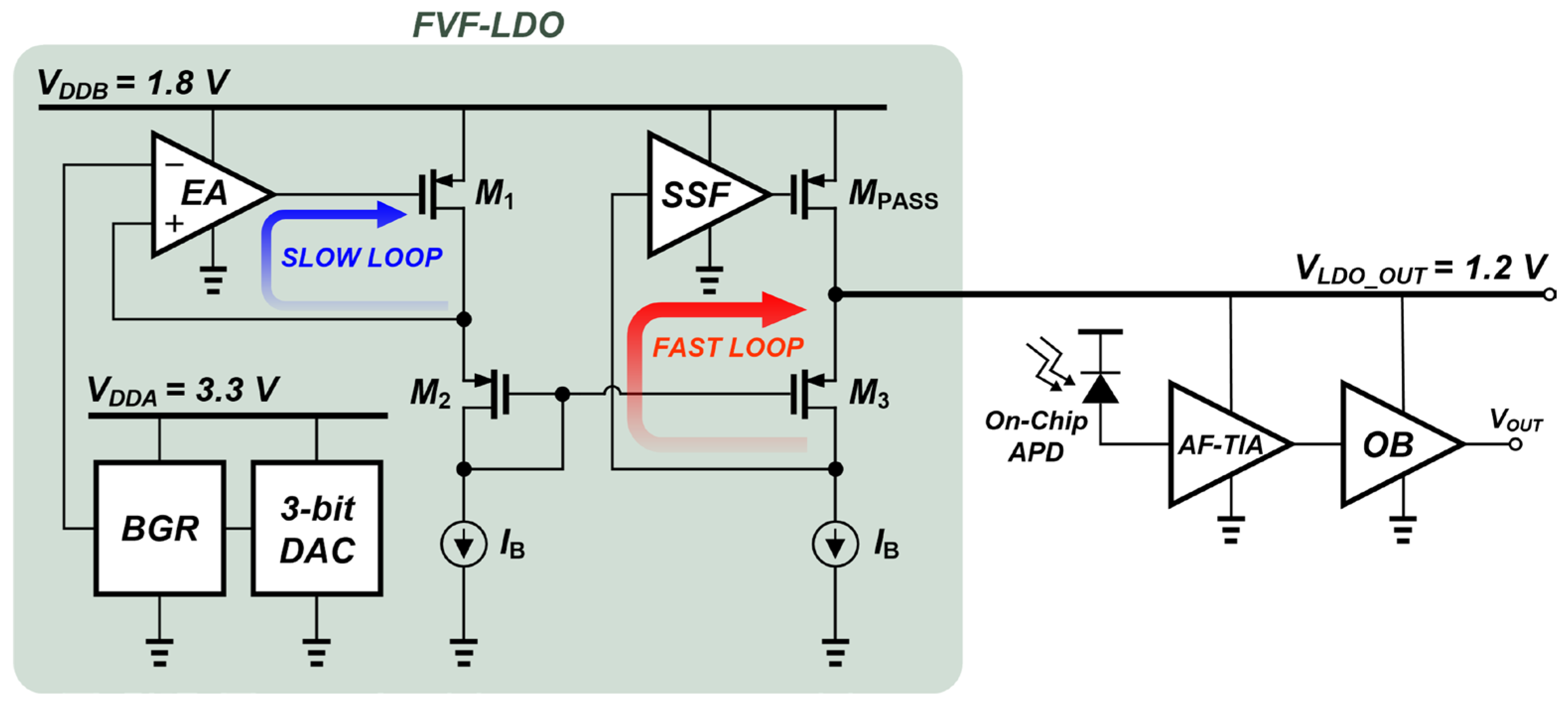
To compensate for these non-idealities, a trimming digital-to-analog converter (DAC) is integrated to enable post-fabrication calibration of the reference voltage, thus improving robustness and accuracy. Moreover, this paper proposes an integrated receiver front-end circuit featuring an inverter-based TIA with an on-chip FVF-based LDO, as shown in Figure 3. The proposed architecture improves the circuit robustness against supply variations while maintaining low power consumption, hence making it well suited for compact and energy-efficient optical receiver applications.

2. Optoelectronic TIA with FVF-Based LDO

2.1. Bandgap Reference with 3-Bit DAC

2.1.1. Bandgap Reference Circuit

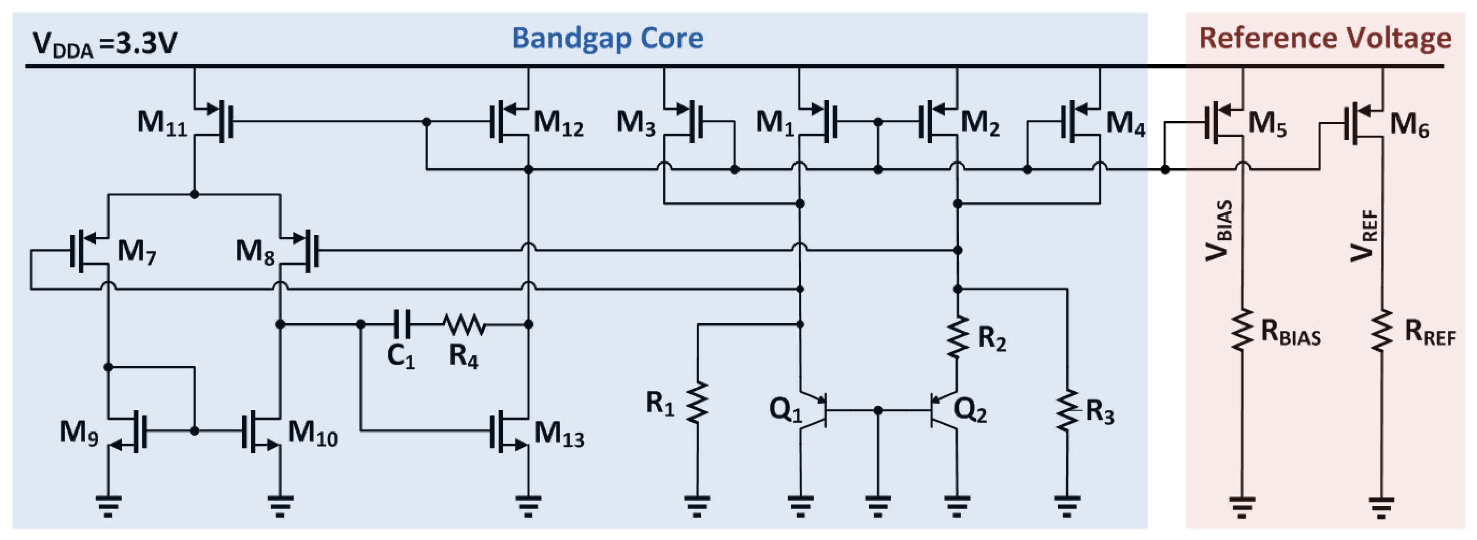
Bandgap reference (BGR) is well known to generate a stable reference voltage for LDOs. Therefore, LDOs can regulate the supply voltage delivered to the load and suppress disturbances caused by load variations. This reference voltage should be insensitive even to severe PVT variations [9]. Figure 4 shows the schematic diagram of the proposed BGR circuit, where two reference voltages ( V R E F and V B I A S ) are generated. The core of the BGR adopts the Brokaw-cell topology, in which two bipolar transistors (Q1 and Q2) with different emitter areas generate a base–emitter voltage difference Δ V B E , which is given by
Δ V B E = V T l n n
where n represents the emitter area ratio between Q1 and Q2.
This voltage difference is applied across the resistor R 2 , thereby generating a proportional-to-absolute-temperature (PTAT) current that is given by
I P T A T = V T l n ( n ) R 2
On the other hand, the base–emitter voltage ( V B E 1 ) exhibits a complementary-to-absolute-temperature (CTAT) characteristic. When applied across the resistor R 3 , it generates a current which can be expressed as
I C T A T = V B E 1 R 3
These currents are mirrored through the PMOS current mirrors and converted into a reference voltage across the resistor R R E F . Therefore, the final reference voltage is given by
V R E F = R R E F V T l n ( n ) R 2 V B E 1 R 3
In this work, two PMOS current-mirror branches are implemented to provide both the reference voltage for the LDO and the bias voltage for internal circuits. By adjusting the resistor ratios in each branch, two stable voltages ( V R E F and V B I A S ) are generated. Furthermore, the supply voltage for the BGR is separated from that of the LDO, effectively isolating the BGR voltage generation from the LDO load variations. This separation helps to minimize the influence of transient currents and enhances the overall circuit stability. Hence, both the LDO reference voltage and the internal bias voltage can maintain high accuracy, while reducing the sensitivity to supply noise effectively.

2.1.2. Trimming DAC Circuit

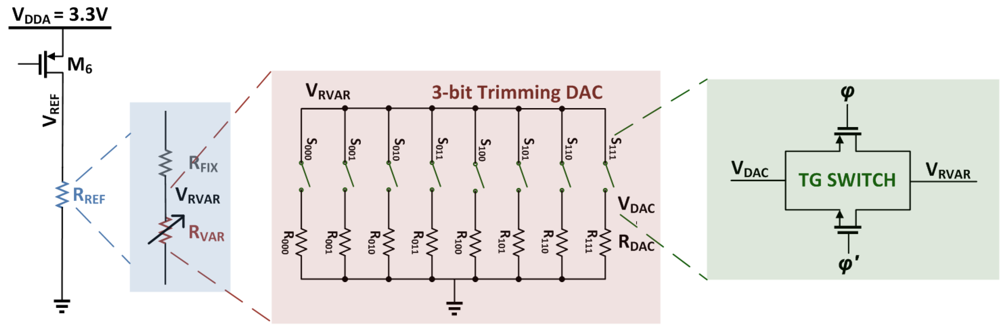
As mentioned above, the BGR circuit must provide a stable reference voltage against the variations in supply voltage and temperature. However, process variations might introduce deviations in the output reference voltage. To compensate for these process-induced variations, a trimming DAC circuit should be incorporated into the proposed design, as depicted in Figure 5.
The overall architecture of the proposed 3-bit trimming DAC employs a 3-to-8 decoder to control a switch array. Accordingly, the decoder outputs selectively activate switches connected to the trimming resistor network, therefore determining the current paths within the network. The trimming resistor network is implemented using parallel resistors with a uniform step size of 600 Ω, allowing the effective resistance to be adjusted from 600 Ω to 4.8 kΩ. By controlling the current flowing through the trimming resistors, the output voltage of the BGR can be finely tuned. This trimming mechanism compensates for the process variations and ensures that the reference voltage remains close to the target value across various chips [10].
Since the trimming DAC operates in a block requiring precise voltage control, accurate voltage transmission through the switches is essential. For this purpose, transmission gate (TG) switches are employed for bit selection. This TG structure enables stable voltage transmission across the entire output voltage range through the complementary operations of the two transistors, thereby mitigating the signal-level-dependent resistance variation that may occur in a single MOS switch. Also, the channel width of the switching transistors is increased to reduce the on-resistance, while the channel length is also enlarged to suppress resistance variations caused by short-channel effects and channel length modulation. Furthermore, increasing the switch device area reduces the device mismatch, thus improving the voltage tuning accuracy of the DAC. Hence, the proposed trimming DAC achieves stable voltage transfer characteristics and improved voltage adjustment accuracy.

2.2. FVF-LDO Regulator with SSF

2.2.1. Circuit Description

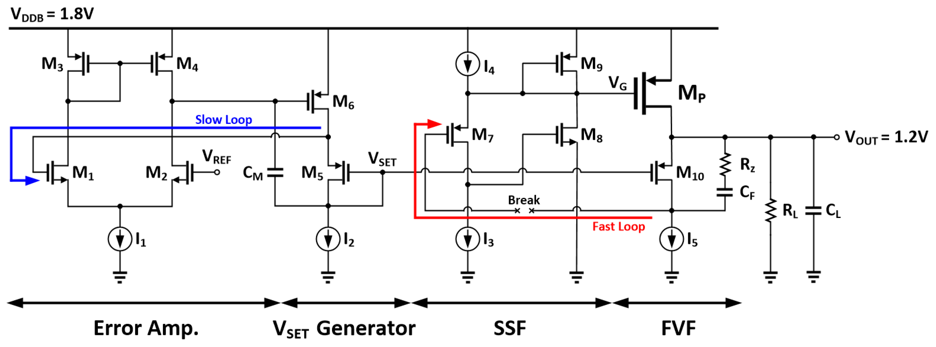
Figure 6 shows the schematic diagram of the proposed flipped-voltage-follower low-dropout regulator (FVF-LDO) with a super-source follower (SSF), consisting of five main building blocks, i.e., an error amplifier ( M 1 M 4 ), a V S E T generator (including M 5 , M 6 , and C 1 ), and an FVF-based output stage ( M 7 M 10 ), the PMOS pass transistor ( M P ), and the feedfowrad network ( R Z C F ). The current sources ( I 1 I 5 ) provide the required bias currents for each sub-block.
In the error amplifier (EA), M 1 and M 2 form the differential input pair while M 3 and M 4 act as active loads. The gate of M 2 is connected to the reference voltage ( V R E F ), and the other input senses the feedback information derived from the output regulation path. Therefore, EA compares the output-related feedback signal with V R E F and generates an error signal that controls the subsequent V S E T node. In other words, this EA block determines the low-frequency regulation accuracy of the LDO [11].
The intermediate generator produces the internal control voltage ( V S E T ). Instead of directly driving the pass-transistor gate from the EA output, the proposed structure first establishes V S E T that serves as the interface between the slow loop and the fast loop [12]. The slow loop determines the desired regulation level, while the fast loop rapidly reacts to load-induced output disturbances. In particular, a capacitor ( C M ) is introduced to shape the frequency response of this node and to stabilize the slow loop.
Transistors M 7 M 10 form the local FVF and SSF structure, and M P acts as the pass-device supplying the load currents from V D D B to V O U T . The output node is loaded by R L and C L , which represent the equivalent load resistance and capacitance seen by the LDO. In addition, the series network R z C F is connected near the output stage to improve the loop stability by introducing a zero and reshaping the non-dominant poles [13,14].
The principal operations of the FVF-LDO can be understood as the combination of a slow loop and a fast loop. The slow loop starts from the EA, passes through the V S E T generator, and determines the long-term DC regulation of the output voltage. In contrast, the fast loop is locally formed by the FVF and SSF around M 7 M 10 and M P , and it rapidly suppresses output variations caused by the load transients. Therefore, the proposed FVF-LDO regulator can achieve accurate output regulation, high stability, and fast transient response simultaneously.

2.2.2. Small Signal Analysis

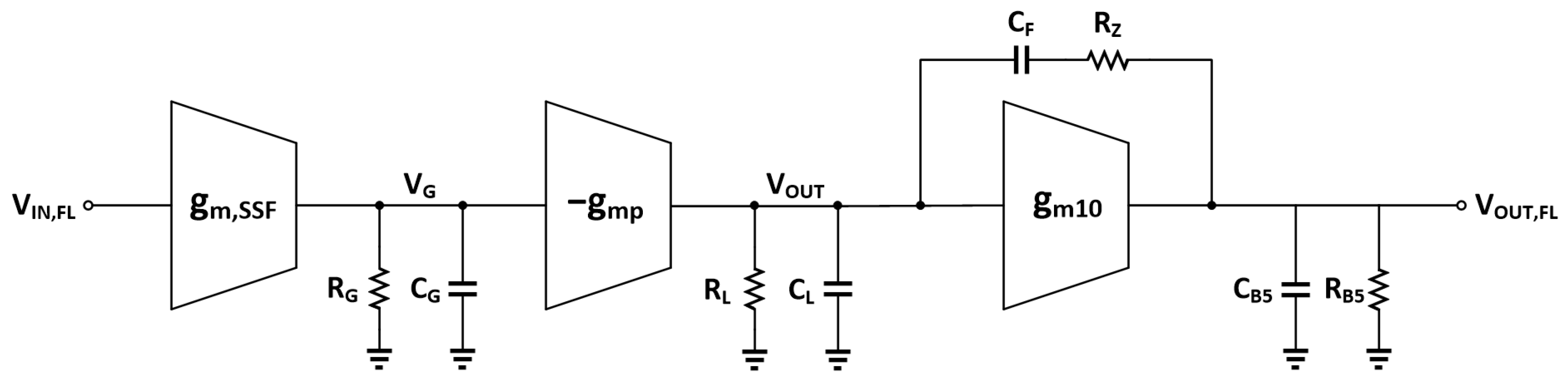
Figure 7 shows the small-signal model of the fast loop in the proposed FVF-LDO, where g m , S S F , g m p , and g m 10 denote the effective transconductance of the SSF block, the transconductance of M p , and the transconductance of M 10 , respectively. Also, R G and C G represent the parastic resistance and capacitance at V G . In addition, R B 5 and C B 5 represent the drain-source resistance and parasitic capacitance of I B 5 .
Based on this small-signal model, the transfer function of the fast loop is given by
H ( s ) = V o u t , F L V i n , F L = g m , S S F g m p g m 10 R G R L R B 5 1 s C F 1 g m 10 R z ( 1 + s R G C G ) 1 s a 1 s 2 a 2 s 3 a 3
where the denominator coefficients are described as follows.
a 1 = R L C L + C F 1 + g m 10 R B 5 + R B 5 C B 5 + C F + C F R z
a 2 = R L R B 5 C L C B 5 + C L C F + C B 5 C F + R z C F R L C L + R B 5 C B 5
a 3 = R L R B 5 R z C L C B 5 C F
Hence, the low-frequency (LF) gain of the fast loop is obtained at s 0 as
A 0 = g m , S S F R G · g m p R L · g m 10 R B 5
It is clearly seen that the LF gain is determined by the cumulative gain contribution of the SSF, the common-source stage, and the common-gate stage. Such a large LF gain enables strong corrective action even for small output-voltage perturbations and directly contributes to suppressing the transfer of supply ripple or disturbance to the output node. Therefore, the large A 0 can be interpreted as one of the key factors supporting the PSRR improvement at low frequencies in the proposed structure [15].
From the numerator of the transfer function, the zero frequency can be written as
z 1 = 1 C F 1 g m 10 R z .
The zero location in (10) is determined by the relative magnitudes of R z and 1 / g m 10 . When R z < 1 / g m 10 , the zero is located in the right-half plane (RHP), whereas it is placed in the left-half plane (LHP) when R z > 1 / g m 10 . When R z = 1 / g m 10 , the zero is pushed to a very high frequency and becomes practically negligible [16]. In this design, R z was chosen such that R z > 1 / g m 10 over the intended operating region so that the zero is placed in the LHP. This helps alleviate the phase degradation caused by non-dominant poles, thus leading to a more favorable phase margin and improved loop stability [17]. The poles can be summarized as follows:
p 1 1 R L C L + C F ( 1 + g m 10 R B 5 ) + R B 5 ( C B 5 + C F ) + C F R z
p 2 = 1 R G C G
p 3 , p 4 :   o b t a i n e d   f r o m   1 + s a 1 + s 2 a 2 + s 3 a 3
where p 1 is the dominant pole associated with V O U T , and both the load capacitance and the feedforward compensation path contribute to the effective time constant. p 2 is the high-frequency pole formed at V G , while p 3 and p 4 , together with p 1 , are the higher-order poles determined from the cubic denominator and reflect the coupled response of V O U T and V O U T , F L . In addition, C F forms the feedforward compensation path and affects the overall pole-zero distribution. If the Miller effect is sufficiently strong, p 1 can be approximated as
p 1 1 R L C F g m 10 R B 5
indicating that the dominant pole is mainly determined by the Miller-amplified compensation capacitance seen at V O U T .
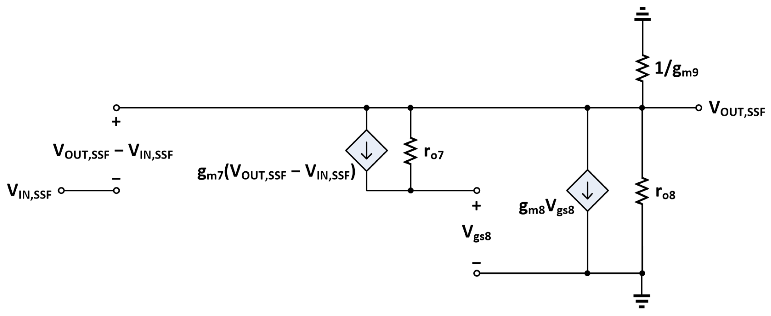
This pole-zero structure is directly related to the PSRR enhancement of the proposed FVF-LDO. Noise components contained in the supply voltage tend to propagate to the output node through the pass transistor [18]. However, the proposed fast loop rapidly senses the output-voltage variations and immediately adjusts the operating condition of the pass transistor through the internal control node. In this process, the large LF gain effectively suppresses the LF supply ripple, while the zero generated by the R z C F compensation path compensates for the phase degradation caused by non-dominant poles in the mid- and high-frequency range, thereby extending the frequency range over which effective supply-noise suppression can be maintained [19]. Furthermore, when the pole at the gate-control node is shifted to sufficiently high frequencies, the charging and discharging speed of the pass-transistor gate is improved, allowing correct action to take place before the supply disturbance is fully transferred to the output. Therefore, the PSRR improvement of the proposed FVF-LDO can be understood as the combined results of large LF gain, fast gate control, and the pole-zero characteristics shaped by the R z C F compensation network. Figure 8 shows the small-signal model of the SSF block, where the effective transconductance of the SSF is given by
g m , S S F = g m 7 r o 7 g m 7 r o 7 + 1 + 1 g m 8 r o 8
R o , S S F 1 g m 8 + g m 7 r o 7 g m 8 + 1 r o 8
where g m 7,8 and r o 7,8 are the transconductance and output resistance of M 7 and M 8 , respectively.
The SSF in the proposed fast loop provides a lower output resistance and stronger gate-driving capability than a conventional source follower (SF). In a conventional SF, the output resistance is fundamentally limited, which restricts the charging and discharging speed when driving the pass-transistor gate with a large parasitic capacitance. This limit slows down the internal control node and eventually constrains the loop bandwidth, the transient response, and the supply-noise rejection capability [20]. By contrast, the proposed SSF can achieve a lower output resistance through its active local feedback, enabling faster drive of the pass-transistor gate. This reduces the driving resistance seen at the gate-control node and shifts the corresponding pole to a higher frequency, which in turn improves both the speed and stability of the fast loop. Such a low output resistance also enhances the charging and discharging speed, thus allowing faster corrective action against the output perturbations and enabling the gate control to respond before supply-voltage variation is fully transferred to the output node. Hence, the SSF in the proposed structure should not be regarded simply as a buffer replacement, but rather as a deliberate choice to overcome the driving limitation of a conventional SF while simultaneously improving the fast loop bandwidth, the transient response, and the PSRR performance.

2.2.3. Power Supply Rejection (PSR)

In the absence of regulation, variations at the supply node are transferred to the output through the finite small-signal resistance ( r d s , p ) of the pass device [21]. In the proposed FVF-LDO, however, the fast loop senses the resulting output variation and adjusts the pass-transistor gate voltage, thus reducing the effective output impedance at the regulated node and suppressing the propagation of the supply noise. The open-loop shunt impedance seen at the output node is given by
Z o , F L ( s ) = 1 1 R L + 1 R B 5 + s ( C L + C B 5 ) .
When R B 5 is sufficiently large and C B 5 is much smaller than C L , it can be approximated as
Z o , F L ( s ) R L 1 s C L .
Since the closed-loop output impedance is reduced by the fast loop gain, the output impedance of the FVF-LDO (in the frequency range where the fast loop gain is sufficiently large) is given by
Z o , L D O ( s ) Z o , F L ( s ) A F L ( s ) .
Substituting this equation into the PSR definition gives
P S R L D O ( s ) = Z o , L D O ( s ) r d s , p + Z o , L D O ( s ) Z o , F L ( s ) / A F L ( s ) r d s , p + Z o , F L ( s ) / A F L ( s ) 1 1 + A F L ( s ) r d s , p Z o , F L ( s )
which clearly reveals that the PSR is determined by two main factors: the output-node open-loop shunt impedance and the fast loop gain [22]. As A F L ( s ) increases, the effective output impedance decreases, and the amount of supply ripple transferred to the output is correspondingly reduced. Therefore, the PSR improvement of the proposed FVF-LDO can be interpreted as the result of the active impedance reduction at the output node by the fast loop. At low frequencies, the output-node impedance is dominated by the load resistance, such that
Z o , F L ( 0 ) R L .
Also, the LF fast loop gain is given by
A F L ( 0 ) = A 0 = g m , S S F R G · g m p R L · g m 10 R B 5 .
Accordingly, the LF PSR (if A 0 1 ) can be approximated as
P S R L D O ( 0 ) 1 1 + A 0 r d s , p R L R L A 0   r d s , p .
This equation indicates that the LF PSR is inversely proportional to the LF fast loop gain, confirming that a larger fast loop gain directly improves the rejection of supply ripple. In the mid- and high-frequency range, the PSR behavior is additionally affected by the compensation path [23]. This path helps to maintain the effectiveness of the fast loop by preventing an abrupt degradation of the loop response, thereby extending the frequency range over which supply-noise suppression is preserved.
In addition, the low output resistance of the SSF enables faster charging and discharging of the pass-transistor gate, which allows the FVF-LDO regulator to respond more quickly to supply disturbances. Consequently, the proposed structure improves PSR by actively lowering the output impedance through fast loop action over a wide frequency range.

2.3. Active-Feedback Transimpedance Amplifier

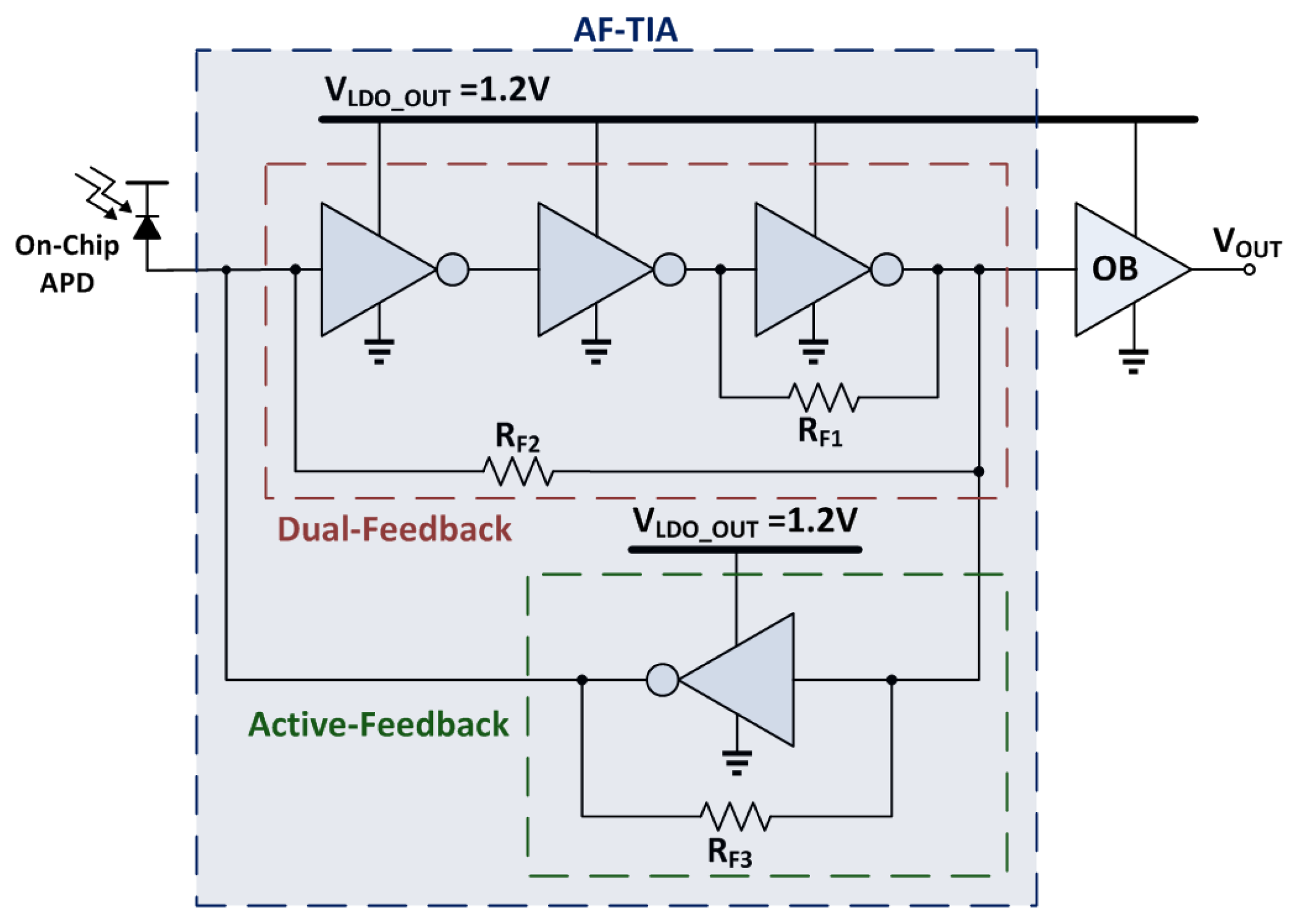
A transimpedance amplifier (TIA) is employed as the front-end circuit of an optical receiver to convert an input photocurrent signal into an output voltage. The input photocurrent is generated by an on-chip P+/N-well avalanche photodiode (APD), which is a previously fabricated and experimentally characterized device reported in [24]. The APD implemented in a 180 nm CMOS process exhibited a responsivity of 2.72 A/W with a junction capacitance of approximately 490 fF. These parameters are based on the measured results from the prior work and are used in this work to enable a realistic device-level evaluation of the proposed receiver front-end. Figure 9 shows the block diagram of the active-feedback transimpedance amplifier that comprises an inverter-based CMOS TIA and an inverter-based output buffer (OB). Both blocks are powered by the proposed FVF-LDO. The TIA topology is based on the one previously described in [25], such that a shunt-feedback inverter-based amplifier stage is followed by an OB.
In this architecture, the inverter-based multi-stage amplifier provides sufficient voltage gain while maintaining a relatively low input resistance that reduces the input current loss and extends the bandwidth. By utilizing the FVF-LDO, the TIA operates with a supply voltage of 1.2 V. It should be noted that the available voltage headroom becomes limited under a reduced supply voltage, making the circuit more susceptible to supply noise and variations. Therefore, stable supply regulation is crucial to ensure reliable operations. Finally, an OB is employed to isolate the load capacitance from the core amplifier and to match the output impedance close to 50 Ω, facilitating standard measurements. This configuration enables convenient interface with external test instruments as well as potential sensor systems.

3. Layout and Simulation Results

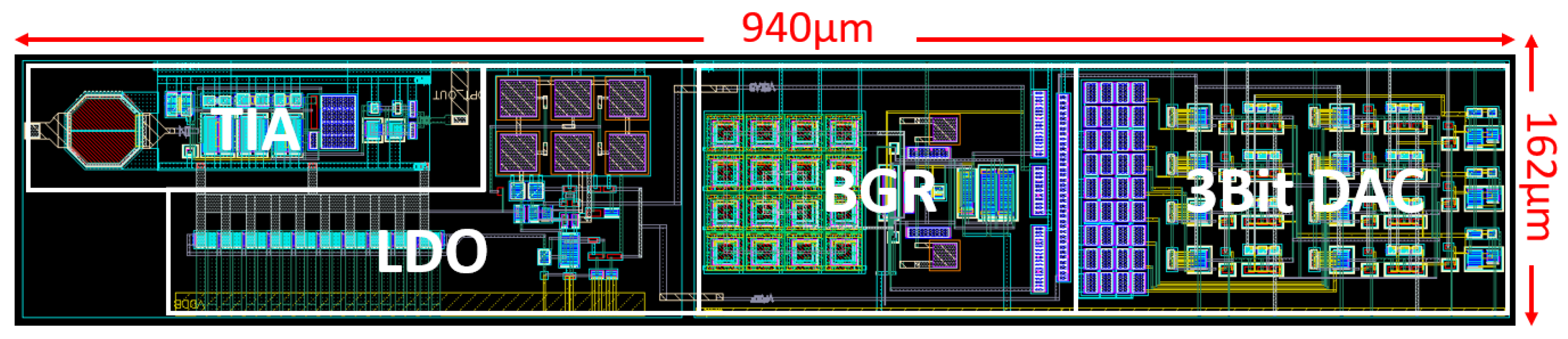
Figure 10 illustrates the layout of the proposed optoelectronic TIA with an FVF-LDO, where the chip core occupies an area of 940 × 162 μ m 2 . Specifically, an on-chip avalanche photodiode was integrated together with the active-feedback TIA not only to facilitate the PC-board designs for testing but also to avoid the unnecessary signal distortions attributed to the well-known inductance effect of bond-wires on chip.
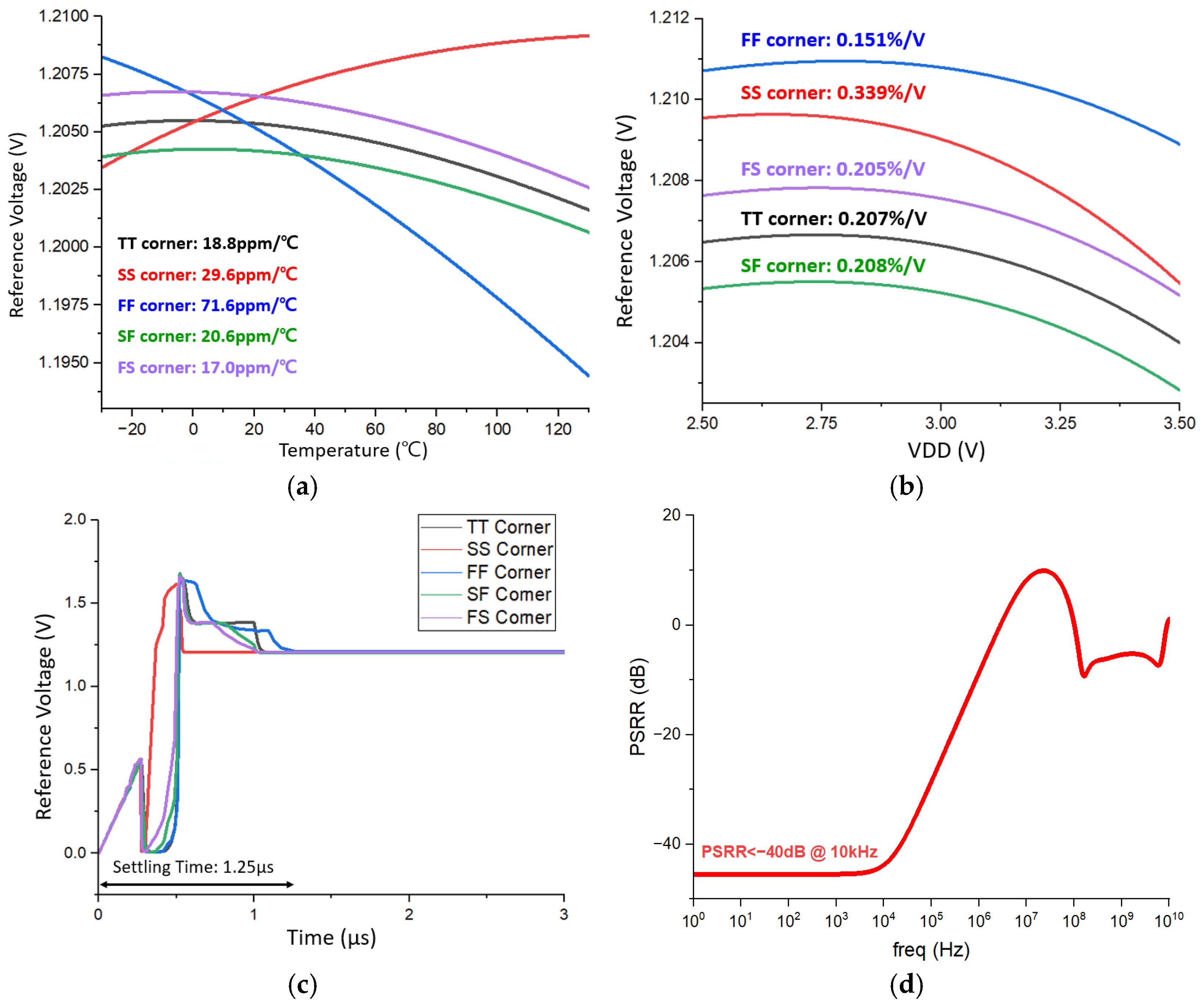
Post-layout simulations were conducted by utilizing the model parameters of a standard 180 nm CMOS process. First, the performance of the proposed BGR with an integrated 3-bit trimming DAC was evaluated through temperature, supply, transient, and power-supply variation simulations across multiple process corners. The trimming DAC provides fine adjustment of the BGR output voltage V R E F to compensate for process variations.
Figure 11a shows the temperature coefficient (TC) of the reference voltage ( V R E F ) over the range of −30 °C to 130 °C. The simulated TC values are 18.8 ppm/°C (TT), 29.6 ppm/°C (SS), 71.6 ppm/°C (FF), 20.6 ppm/°C (SF), and 17.0 ppm/°C (FS), respectively.
These results indicate that the 3-bit trimming DAC effectively stabilizes V R E F across corners, with the FF corner exhibiting slightly higher variation. Figure 11b presents the line regulation of V R E F , obtained by sweeping the supply voltage V D D from 2.5 V to 3.5 V. The simulated deviations are 0.207%/V (TT), 0.339%/V (SS), 0.151%/V (FF), 0.208%/V (SF), and 0.205%/V (FS), demonstrating the robust immunity of the BGR output to the supply voltage fluctuations across all corners. In Figure 11c, the dynamic performance of V R E F is assessed through transient simulations with a 1 µs ramp input. The output voltage is settled within 1.25 µs in all the process corners, confirming fast and stable startup behavior. Figure 11d depicts the power supply rejection ratio (PSRR) of the BGR with the trimming DAC, achieving a PSRR of −45.5 dB. Despite the presence of the switching network and TG-based circuitry, the PSRR remains adequate for practical applications. Overall, these post-layout simulation results demonstrate that the proposed BGR with the integrated TG-based trimming DAC provides stable reference voltage generation across process, voltage, and temperature variations.
.
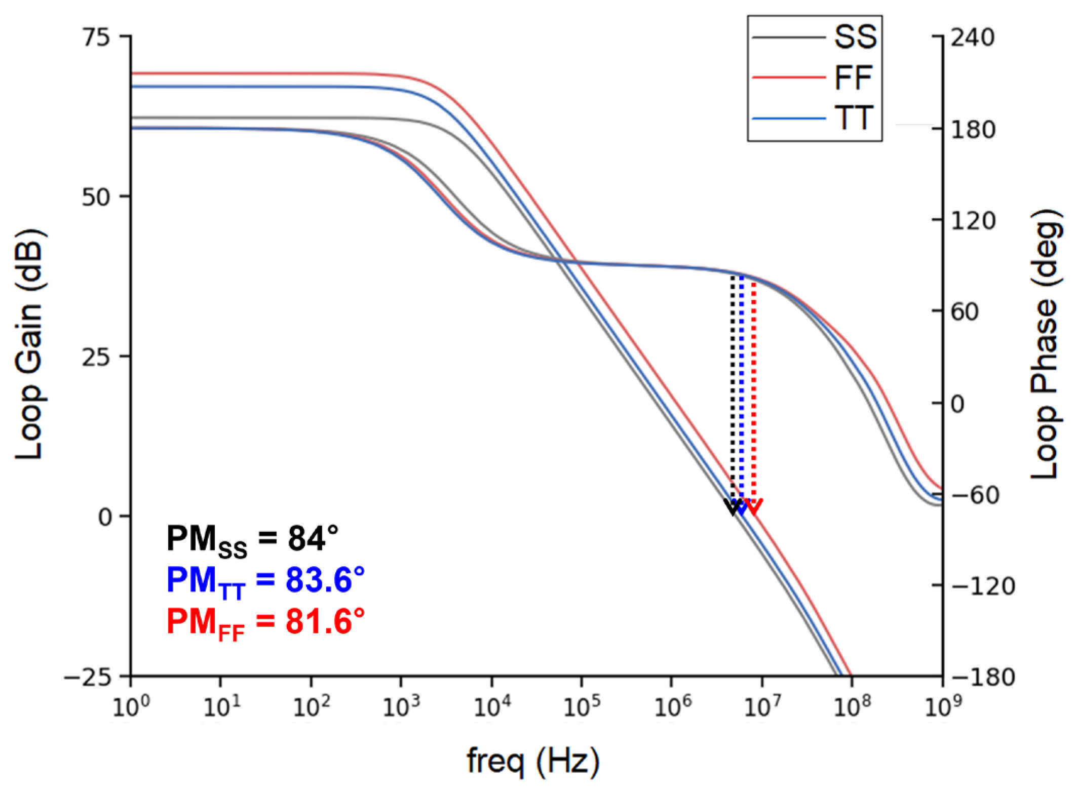
The frequency response of the slow loop and fast loop of the proposed FVF-LDO is shown in Figure 12 and Figure 13, respectively. All results were evaluated under the SS, TT, and FF process corners. In the slow loop response of Figure 12, the phase margins are 84 ° , 83.6 ° , and 81.6 ° at the SS, TT, and FF corners, respectively, indicating sufficient stability margin. Also, these values remain the same under both light load and heavy load conditions. Furthermore, the variation across process corners is small, demonstrating that the proposed structure operates stably against both load and process variations.
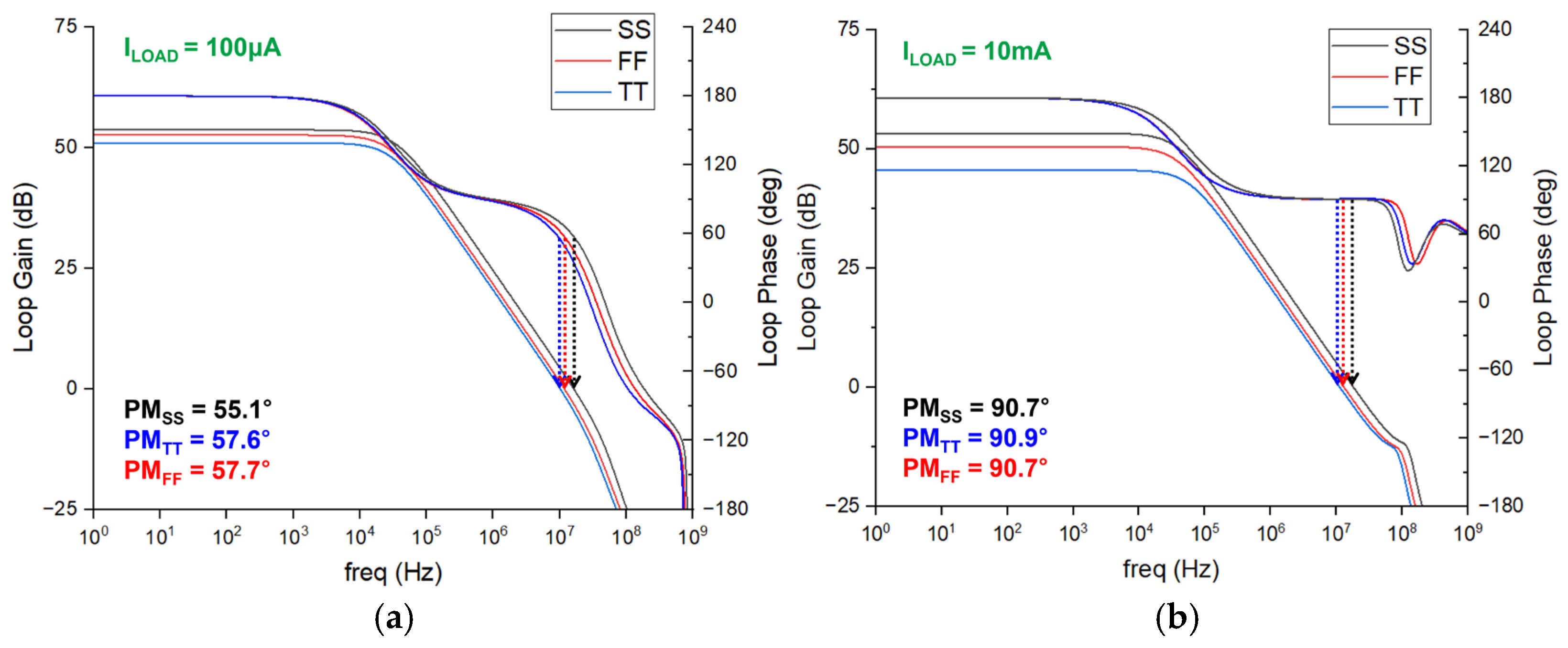
For the fast loop, the phase margins under the light load condition are 55.1 ° , 57.6 ° , and 57.7 ° for the SS, TT, and FF corners, respectively, confirming sufficient stability margin even at light load. Under the heavy load condition, the phase margins are 90.7 ° , 90.9 ° , and 90.7 ° respectively, therefore showing a larger stability margin than in the light load case. Moreover, the variation in phase margin across process corners is small in both load conditions, indicating that the proposed structure maintains stable operation against process variation. These results confirm that both the slow loop and fast loop of the proposed dual-loop FVF-LDO maintain sufficient stability margin over a wide load range and across process corners.
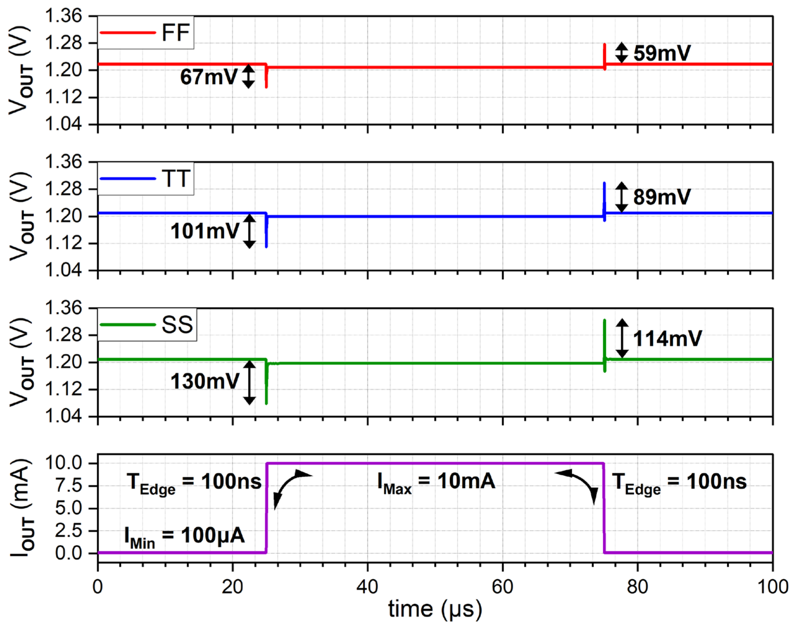
Figure 14 shows the load transient response of the FVF-LDO, where the load current varies between 100   μ A and 10   m A , with both the rising and falling edge times set to 100   n s . Under this condition, the undershoot and overshoot are 67   m V and 59   m V at the FF corner, 101   m V and 89   m V at the TT corner, and 130   m V and 114   m V at the SS corner, respectively. Although the magnitudes of the output-voltage variation differ across process corners, the output voltage quickly returns to its steady-state value without severe ringing in all PVT corners. This demonstrates that the proposed fast loop effectively controls the pass-transistor gate during abrupt load current changes while maintaining sufficient damping.
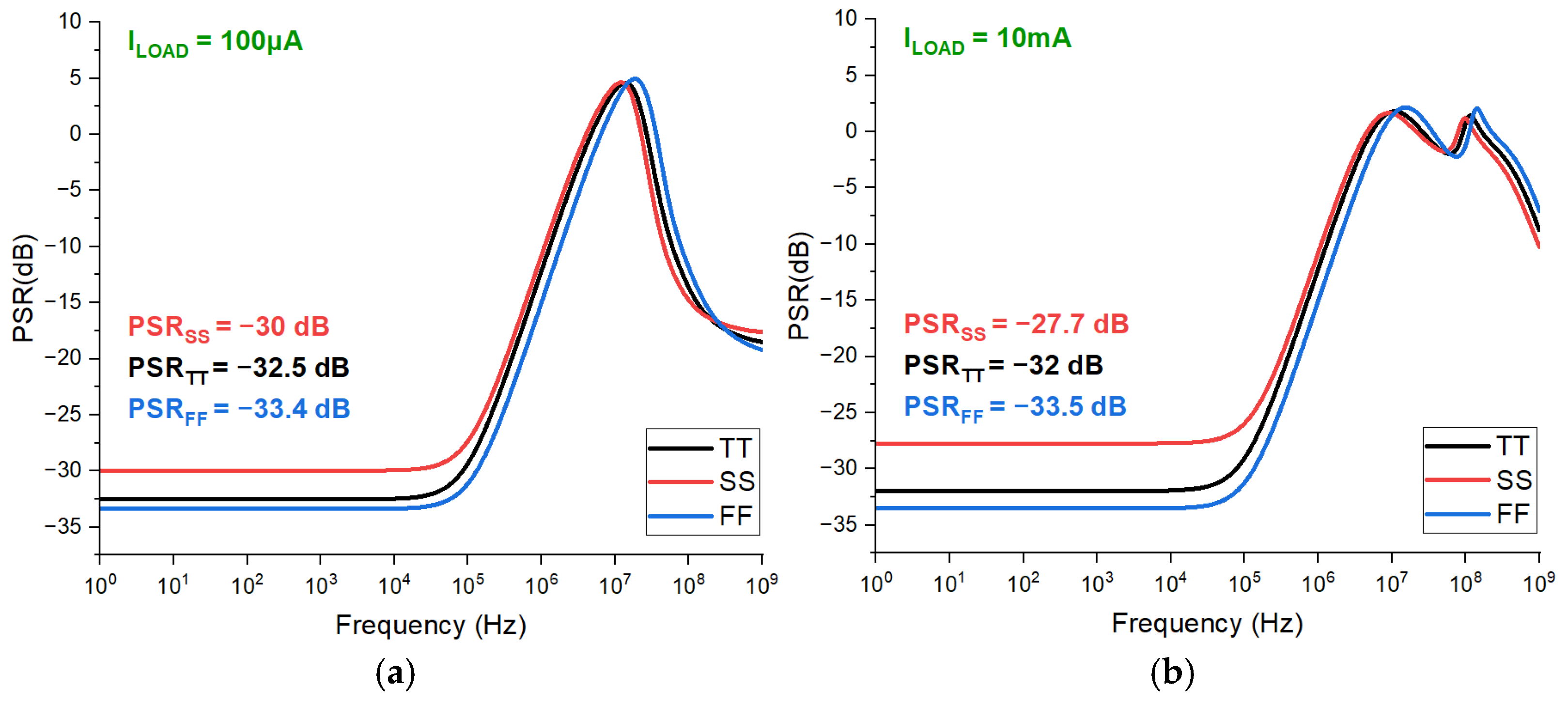
Figure 15 shows the simulated PSR characteristics of the proposed FVF-LDO under different load current conditions and process corners. For the PSR simulations, the BGR was biased with a constant supply, while the supply ripple was injected only into the LDO supply. Under the light load condition, the low-frequency PSR is 30   d B , 32.5   d B , and 33.4   d B for the SS, TT, and FF corners, respectively, while under the heavy load condition, the corresponding values are 27.7   d B , 32   d B , and 33.5   d B , respectively. The low-frequency PSR is mainly determined by the low-frequency fast loop gain. As the frequency increases, the PSR degrades due to the reduction in loop gain. The peaking observed in the mid- and high-frequency range may be attributed to the pole-zero characteristics of the internal loop. These results show that the PSR of the proposed FVF-LDO is determined by both the fast loop gain and its frequency response characteristics.
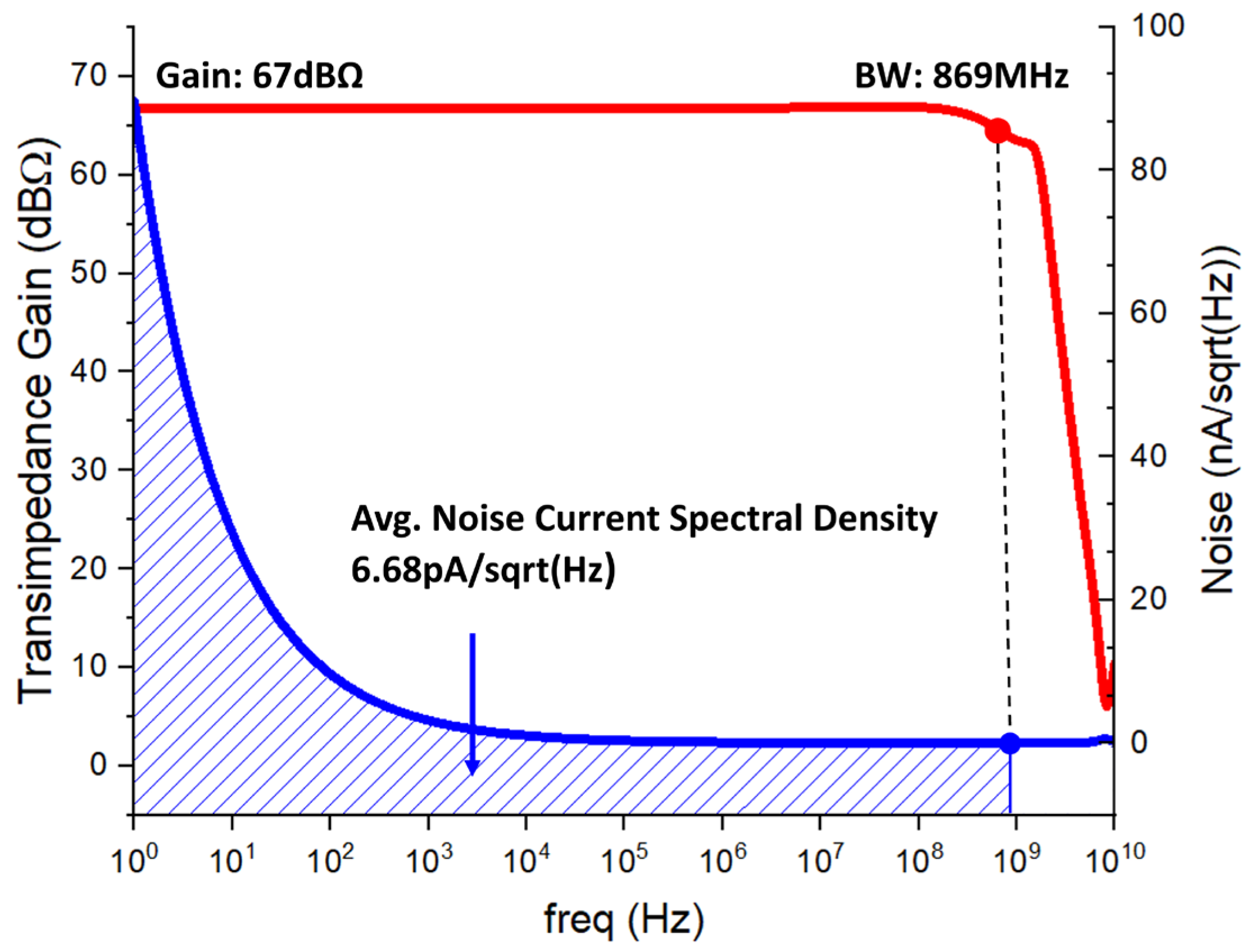
Figure 16 shows the post-layout simulation results of the proposed optoelectronic TIA, achieving a transimpedance gain of 67 dBΩ, a −3 dB bandwidth of 869 MHz, and an average input-referred noise current spectral density of 6.68 pA/√Hz over the frequency range of interest.
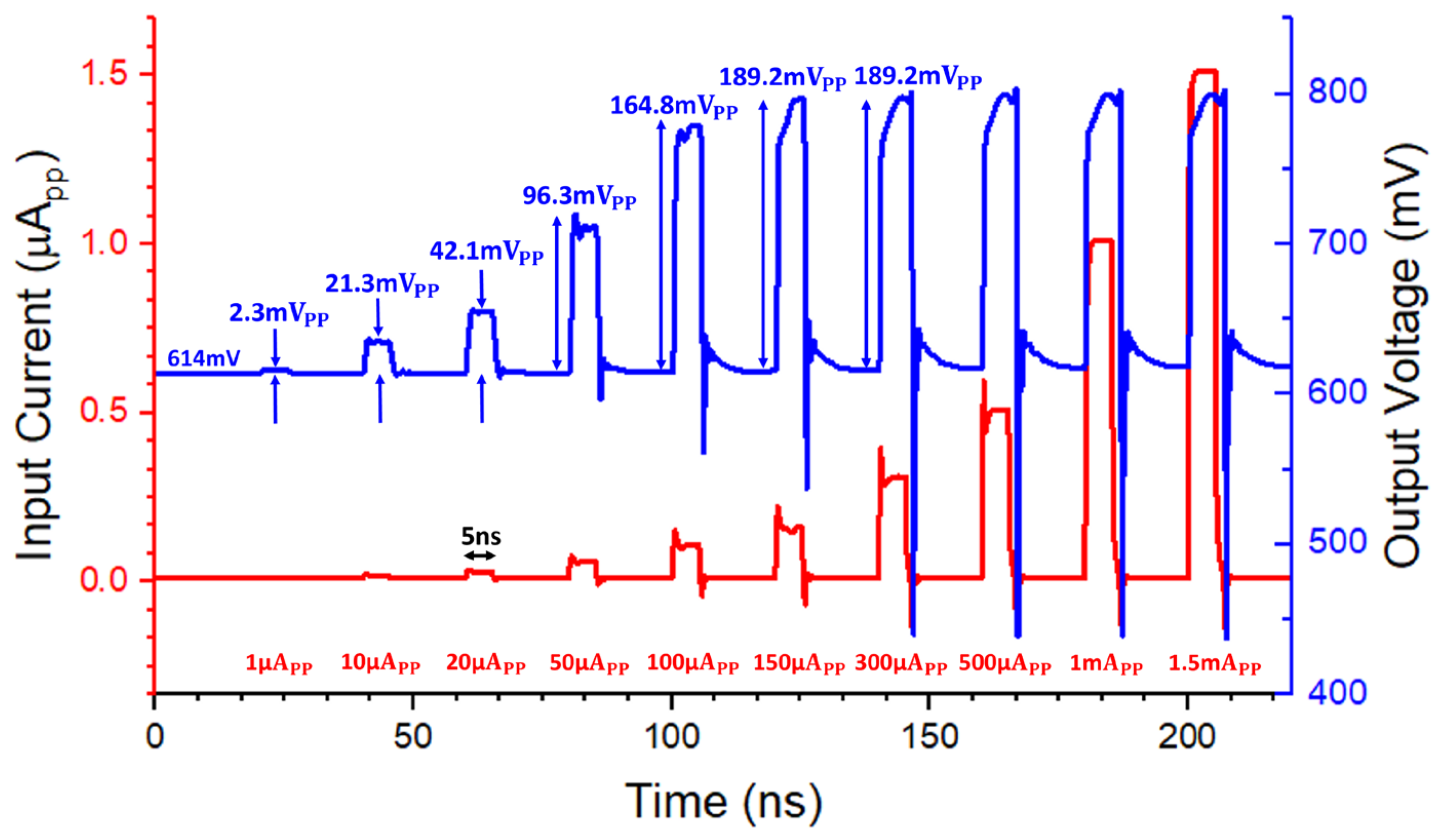
Figure 17 illustrates the simulated pulse response of the proposed optoelectronic TIA under varying input current amplitudes ranging from 1 μApp to 1.5 mApp. As the input current increases, the output voltage amplitude correspondingly increases. However, beyond 150 μApp, the output pulse amplitude begins to saturate and remains nearly constant for larger input currents.
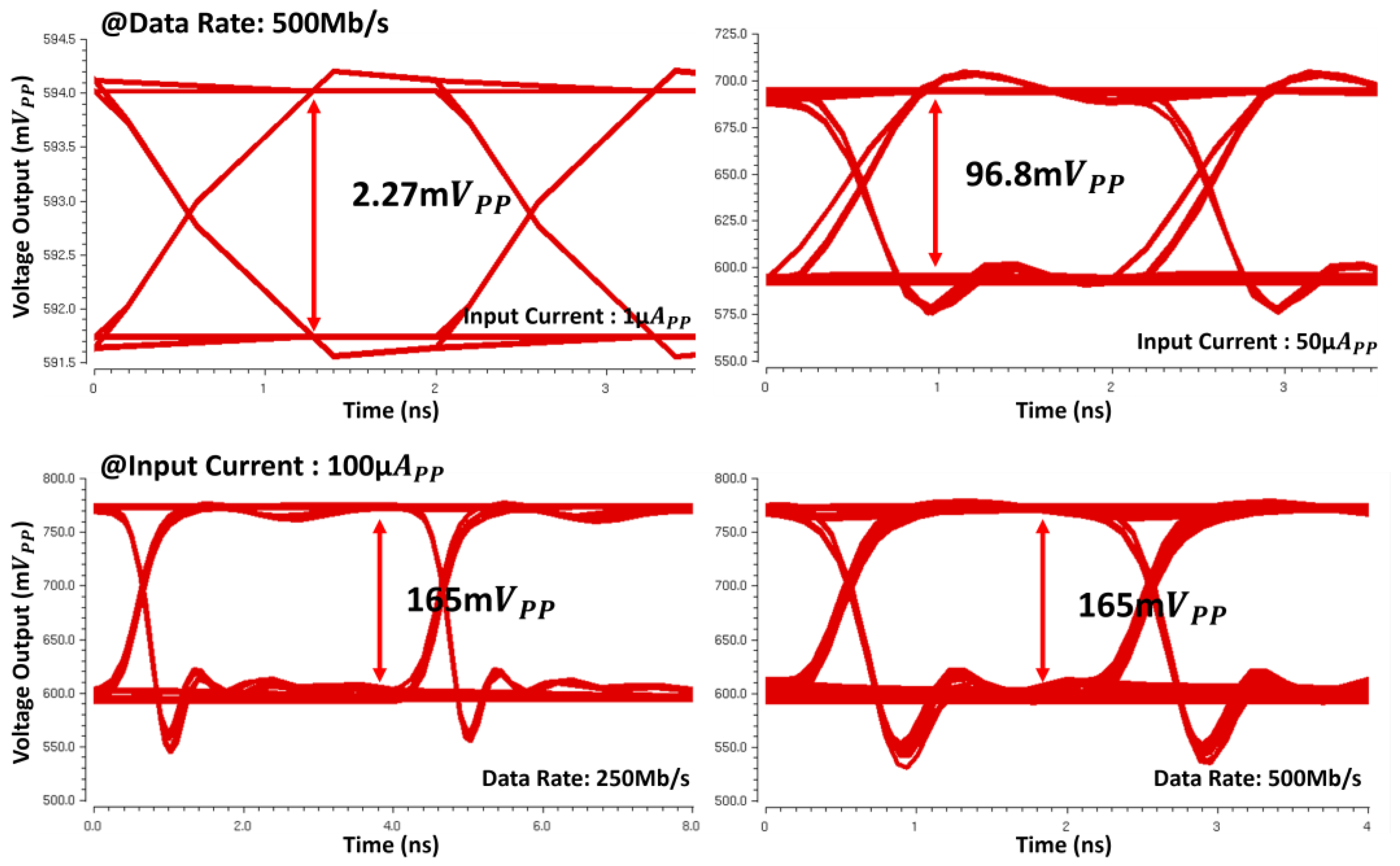
Figure 18 shows the simulated eye-diagrams of the proposed optoelectronic TIA under the different input current levels and data rates. At a fixed data rate of 500 Mb/s, the simulated eye-diagrams are presented for two input currents of 1 μApp and 50 μApp, respectively. Although slight fluctuations are observed, the eye-openings remain clearly distinguishable in both cases.
With the input current amplitude fixed at 100 μApp, the eye-diagrams at the two different data rates of 250 Mb/s and 500 Mb/s exhibit consistently open eyes, indicating stable signal integrity across the evaluated data rates.
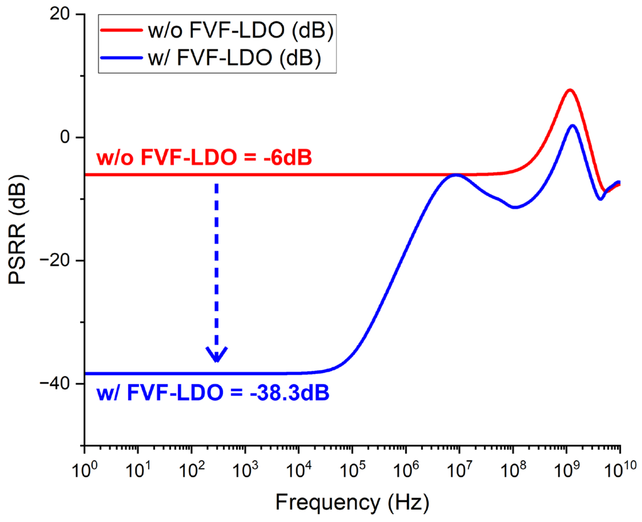
Figure 19 compares the PSRR of the proposed TIA with and without the on-chip FVF-LDO. The TIA with the FVF-LDO shows an improvement of ~30 dB in PSRR when compared to the case without the FVF-LDO. This confirms that the inclusion of the on-chip FVF-LDO effectively reduces the supply noise and therefore enhances the robustness of the TIA against supply variations.
Table 1 compares the performance of the proposed optoelectronic TIA with prior CMOS works. Ref. [26] realized a differential optical receiver in a 28 nm CMOS, targeting high-speed operations with a wideband TIA featuring high power supply rejection. However, the power dissipation per channel was considerable, and the noise current spectral density was also relatively high, therefore demonstrating its limited applicability in low-power, low-noise optical interconnects.
Ref. [27] employed an off-chip PIN photodiode with a wideband TIA for high-speed operations. However, the inherently low responsivity of the PIN photodiode degraded the achievable sensitivity, thus requiring relatively high optical input power. Moreover, the bandwidth-oriented design constrained the transimpedance gain, reducing its effectiveness in low signal conditions. In addition, the usage of a wire-bonded photodiode introduced parasitic effects, leading to signal distortion and increased system complexity.
Ref. [28] presented a single-ended optical receiver using an off-chip photodiode in a 130 nm CMOS, achieving a similar transimpedance gain to this work. Yet, the bandwidth was significantly higher, approximately ten times wider. Therefore, the noise current spectral density was relatively high and the power dissipation per channel was excessive, over four times that of the proposed optoelectronic TIA. This would limit its suitability for energy-efficient optical interconnect applications.
Ref. [29] reported a fully differential optical receiver in a 130 nm CMOS, showing a high transimpedance gain. The differential architecture enabled a PSRR of −23 dB even without an on-chip LDO. However, the absence of on-chip regulation led to limited PSRR and higher power consumption.
Ref. [30] suggested a differential optical receiver in a 180 nm CMOS using an off-chip equivalent photodiode. The design demonstrated a very high PSRR of −61 dB, revealing excellent supply-noise rejection performance. However, this enhancement was achieved at the cost of substantial power consumption (153 mW). These results confirm the tradeoff between high PSRR and energy efficiency in differential architectures.
On the contrary, the proposed optoelectronic TIA integrates an on-chip LDO and an on-chip avalanche photodiode (APD) in a 180 nm CMOS. This approach enables the effective suppression of supply noise through local regulation while maintaining low-noise operations at the input stage. In addition, the on-chip integration of the photodiode eliminates the parasitic effects associated with off-chip bond-wire interconnections, thereby reducing signal distortion and system complexity. In consequence, the proposed optoelectronic TIA architecture provides a balanced solution in terms of low noise, low power consumption, and enhanced supply-noise rejection for optical receiver applications.

4. Conclusions

This paper presents an integrated chip-level solution combining an optoelectronic TIA with an on-chip LDO. The proposed system employs an FVF-based LDO whose output voltage is directly determined by the reference voltage ( V R E F ). To ensure accurate regulation under process variations, a BGR with an integrated 3-bit trimming DAC is incorporated, enabling the precise tuning of V R E F and consequently a stable LDO output voltage. By incorporating the on-chip FVF-LDO, the proposed optoelectronic TIA achieves low-noise performance even under low-power operation, while significantly improving immunity to supply noise. The optoelectronic TIA demonstrates an improvement of more than 30 dB in PSRR compared to the baseline condition. Post-layout simulation results verify that the proposed optoelectronic TIA provides a stable and reliable analog front-end solution, achieving low noise, enhanced PSRR, and robust operation under the severe PVT variations. Hence, the proposed architecture is well suited for low-power and high-sensitivity optical receiver applications.

Author Contributions

Conceptualization, S.-M.P.; methodology, S.-M.P.; software, S.C. (Suwon Cho) and S.C. (Sieun Choi); validation, S.C. (Suwon Cho) and S.C. (Sieun Choi); formal analysis, S.C. (Suwon Cho), S.C. (Sieun Choi), and S.-M.P.; investigation, S.C. (Suwon Cho), S.C. (Sieun Choi), and S.-M.P.; writing—original draft preparation, S.C. (Suwon Cho), S.C. (Sieun Choi), and S.-M.P.; writing—review and editing, S.C. (Suwon Cho), S.C. (Sieun Choi), and S.-M.P.; visualization, S.C. (Suwon Cho) and S.C. (Sieun Choi); supervision, S.-M.P.; project administration, S.-M.P.; funding acquisition, S.-M.P. All authors have read and agreed to the published version of the manuscript.

Funding

This work was supported by an IITP (Institute of Information & Communications Technology Planning & Evaluation)-ITRC (Information Technology Research Center) grant funded by the Korea government (Ministry of Science and ICT) (IITP-2026-RS-2020-II201847). This research was supported by a Global—Learning & Academic research institution for Master’s·PhD students, and Postdocs (G-LAMP) Program of the National Research Foundation of Korea (NRF) grant funded by the Ministry of Education (No. RS-2025-25442252).

Data Availability Statement

Data are contained within the article.

Acknowledgments

The EDA tools, Cadence Virtuoso (IC6.1.6) and Siemens Calibre (v2014.3_16.15), were supported by the IC Design Education Center (IDEC), Republic of Korea.

Conflicts of Interest

The authors declare no conflicts of interest.

References

  1. Razavi, B. Design of Integrated Circuits for Optical Communications; McGraw-Hill: New York, NY, USA, 2003. [Google Scholar]
  2. Ramli, A.; Idrus, S.M.; Supa’at, A.S.M. Optical Wireless Front-End Receiver Design. In Proceedings of the 2008 IEEE International RF and Microwave Conference, Kuala Lumpur, Malaysia, 2–4 December 2008; pp. 331–334. [Google Scholar]
  3. Daneshgar, S.; Li, H.; Kim, T.; Balamurugan, G. A 128 Gb/s, 11.2 mW Single-Ended PAM4 Linear TIA with 2.7 μArms Input Noise in 22 nm FinFET CMOS. IEEE J. Solid-State Circuits 2022, 57, 1397–1408. [Google Scholar] [CrossRef]
  4. Park, K.; Oh, W.-S. A 40-Gb/s 310-fJ/b Inverter-Based CMOS Optical Receiver Front-End. IEEE Photonics Technol. Lett. 2015, 27, 1931–1933. [Google Scholar] [CrossRef]
  5. Milliken, R.J.; Silva-Martinez, J.; Sanchez-Sinencio, E. Full On-Chip CMOS Low-Dropout Voltage Regulator. IEEE Trans. Circuits Syst. I Reg. Pap. 2007, 54, 1879–1890. [Google Scholar] [CrossRef]
  6. Akbari, M.; Hussein, S.M.; Hashim, Y.; Tang, K.-T. An Enhanced Input Differential Pair for Low-Voltage Bulk-Driven Amplifiers. IEEE Trans. Very Large Scale Integr. (VLSI) Syst. 2021, 29, 1601–1611. [Google Scholar] [CrossRef]
  7. Pereira-Rial, Ó.; López, P.; Carrillo, J.M.; Brea, V.M.; Cabello, D. An 11 mA Capacitor-Less LDO with 3.08 nA Quiescent Current and SSF-Based Adaptive Biasing. IEEE Trans. Circuits Syst. II Express Briefs 2022, 69, 844–848. [Google Scholar] [CrossRef]
  8. Banba, H.; Shiga, H.; Umezawa, A.; Miyaba, T.; Tanzawa, T.; Atsumi, S.; Sakui, K. A CMOS Bandgap Reference Circuit with Sub-1-V Operation. IEEE J. Solid-State Circuits 1999, 34, 670–674. [Google Scholar] [CrossRef]
  9. Razavi, B. Design of Analog CMOS Integrated Circuits; McGraw-Hill: New York, NY, USA, 2001. [Google Scholar]
  10. Vilella, E.; Diéguez, A. Design of a Bandgap Reference Circuit with Trimming for Operation at Multiple Voltages and Tolerant to Radiation in 90 nm CMOS Technology. In Proceedings of the 2010 IEEE Computer Society Annual Symposium on VLSI, Lixouri, Greece, 5–7 July 2010; pp. 269–272. [Google Scholar]
  11. Ming, X.; Kuang, J.-J.; Gong, X.-C.; Lin, Z.; Xiong, J.; Qin, Y.; Wang, Z.; Zhang, B. A Fast-Transient Capacitorless LDO with Dual Paths Active-Frequency Compensation Scheme. IEEE Trans. Power Electron. 2022, 37, 10332–10347. [Google Scholar] [CrossRef]
  12. Man, T.Y.; Leung, K.N.; Leung, C.Y.; Mok, P.K.T.; Chan, M. Development of Single-Transistor-Control LDO Based on Flipped Voltage Follower for SoC. IEEE Trans. Circuits Syst. I Regul. Pap. 2008, 55, 1392–1401. [Google Scholar] [CrossRef]
  13. Huang, M.; Feng, H.; Lu, Y. A Fully Integrated FVF-Based Low-Dropout Regulator with Wide Load Capacitance and Current Ranges. IEEE Trans. Power Electron. 2019, 34, 11880–11888. [Google Scholar] [CrossRef]
  14. Zhao, J.; Gao, Y.; Zhang, T.-T.; Son, H.; Heng, C.-H. A 310-nA Quiescent Current 3-fs-FoM Fully Integrated Capacitorless Time-Domain LDO with Event-Driven Charge Pump and Feedforward Transient Enhancement. IEEE J. Solid-State Circuits 2021, 56, 2924–2933. [Google Scholar] [CrossRef]
  15. Jang, J.-H.; Gwon, H.-D.; Kong, T.-H.; Yang, J.-H.; Choi, B.-D. A 0.5–1 V, −68 dB Power Supply Rejection Capacitorless Analog LDO Using Voltage-to-Time Conversion in 28-nm CMOS. IEEE J. Solid-State Circuits 2022, 57, 2462–2473. [Google Scholar] [CrossRef]
  16. Park, H.; Jung, W.; Kim, M.; Lee, H.-M. A Wide-Load-Range and High-Slew Capacitor-Less NMOS LDO with Adaptive-Gain Nested Miller Compensation and Pre-Emphasis Inverse Biasing. IEEE J. Solid-State Circuits 2023, 58, 2696–2708. [Google Scholar] [CrossRef]
  17. Zhao, X.; Zhang, Q.; Xin, Y.; Li, S.; Yu, L. A High-Efficiency Fast-Transient LDO with Low-Impedance Transient-Current Enhanced Buffer. IEEE Trans. Power Electron. 2022, 37, 8976–8987. [Google Scholar] [CrossRef]
  18. Chyan, T.Y.; Ramiah, H.; Hatta, S.W.M.; Lai, N.S.; Lim, C.C.; Chen, Y.; Mak, P.-I.; Martins, R.P. Evaluation and Perspective of Analog Low-Dropout Voltage Regulators: A Review. IEEE Access 2022, 10, 114469–114489. [Google Scholar] [CrossRef]
  19. Joshi, K.; Manandhar, S.; Bakkaloglu, B. A 5.6 μA Wide Bandwidth, High Power Supply Rejection Linear Low-Dropout Regulator with 68 dB of PSR up to 2 MHz. IEEE J. Solid-State Circuits 2020, 55, 2151–2160. [Google Scholar] [CrossRef]
  20. Surkanti, P.R.; Garimella, A.; Furth, P.M. Flipped Voltage Follower Based Low Dropout (LDO) Voltage Regulators: A Tutorial Overview. In Proceedings of the 2018 31st International Conference on VLSI Design and 2018 17th International Conference on Embedded Systems (VLSID), Pune, India, 6–10 January 2018; pp. 232–237. [Google Scholar]
  21. Chen, F.; Lu, Y.; Mok, P.K.T. Transfer Function Analysis of the Power Supply Rejection Ratio of Low-Dropout Regulators and the Feed-Forward Ripple Cancellation Scheme. IEEE Trans. Circuits Syst. I Regul. Pap. 2022, 69, 3061–3073. [Google Scholar] [CrossRef]
  22. Cai, G.; Lu, Y.; Zhan, C.; Martins, R.P. A Fully Integrated FVF LDO with Enhanced Full-Spectrum Power Supply Rejection. IEEE Trans. Power Electron. 2021, 36, 4326–4337. [Google Scholar] [CrossRef]
  23. Lavalle-Aviles, F.; Torres, J.; Sánchez-Sinencio, E. A High Power Supply Rejection and Fast Settling Time Capacitor-Less LDO. IEEE Trans. Power Electron. 2019, 34, 474–484. [Google Scholar] [CrossRef]
  24. Joo, J.-E.; Lee, M.-J.; Park, S.M. A CMOS Fully Differential Optoelectronic Receiver for Short-Range LiDAR Sensors. IEEE Sens. J. 2023, 23, 4930–4939. [Google Scholar] [CrossRef]
  25. Park, S.; Lee, S.; Seo, B.; Choi, Y.; Song, Y.; Chon, Y.; Choi, S.; Park, S.-M. A CMOS inverter-based active feedback transimpedance amplifier. Photonics 2024, 11, 617. [Google Scholar] [CrossRef]
  26. Zhou, C.; Huang, W.; Zhang, Y.; Guo, Z.; Li, D.; Gui, X.; Fan, S.; Wang, X.; Geng, L. A Robust Differential 4×28Gb/s Stacked Optical Receiver in 28 nm CMOS Realizing Crosstalk Suppression and Power Supply Rejection. In Proceedings of the 2019 IEEE International Conference on Integrated Circuits, Technologies and Applications (ICTA), Chengdu, China, 13–15 November 2019. [Google Scholar]
  27. Pan, Q.; Wang, Y.; Yue, C.P. A 42-dBΩ 25-Gb/s CMOS Transimpedance Amplifier with Multiple-Peaking Scheme for Optical Communications. IEEE Trans. Circuits Syst. II Exp. Briefs 2020, 67, 72–76. [Google Scholar]
  28. Zeng, J.-R.; Zhou, Y.; Zou, W.-H. A 10-Gb/s Low-Noise and Low-Crosstalk Transimpedance Amplifier Designed in 130-nm BiCMOS. In Proceedings of the 2022 10th International Symposium on Next-Generation Electronics (ISNE), Wuxi, China, 12–14 May 2023. [Google Scholar]
  29. Park, Y.; Kim, J.-H.; Park, S.M. Bootstrapped Fully Differential CMOS Transimpedance Amplifier. J. Semicond. Technol. Sci. 2020, 20, 1–7. [Google Scholar] [CrossRef]
  30. Wang, X.; Ma, R.; Li, D.; Hu, J.; Zhu, Z. A Wide Dynamic Range Analog Front-End with Reconfigurable Transimpedance Amplifier for Direct ToF LiDAR. IEEE Trans. Circuits Syst. II Express Briefs 2023, 70, 1076–1080. [Google Scholar] [CrossRef]
Figure 1. Block diagram of a LiDAR sensor system.
Electronics 15 01771 g001
Figure 2. Supply noises in TIA (a) w/o LDO and (b) w/LDO.
Electronics 15 01771 g002
Figure 3. Block diagram of the proposed optical receiver front-end.
Electronics 15 01771 g003
Figure 4. Schematic diagram of the proposed BGR circuit.
Electronics 15 01771 g004
Figure 5. Simplified architecture of the proposed 3-bit trimming DAC.
Electronics 15 01771 g005
Figure 6. Schematic diagram of the FVF-LDO with SSF.
Electronics 15 01771 g006
Figure 7. Small-signal model of the fast loop in the FVF-LDO with SSF.
Electronics 15 01771 g007
Figure 8. Small-signal model of the SSF.
Electronics 15 01771 g008
Figure 9. Block diagram of the active-feedback TIA.
Electronics 15 01771 g009
Figure 10. Layout of the proposed optoelectronic TIA.
Electronics 15 01771 g010
Figure 11. Simulated results of the proposed BGR across TT, SS, FF, SF, and FS corners: (a) TC of the reference voltage from −30 °C to 130 °C. (b) Line regulation with VDD ranging from 2.5 V to 3.5 V. (c) Startup transient response across TT, SS, FF, SF, and FS corners. (d) PSRR of V R E F .
Electronics 15 01771 g011
Figure 12. Simulated frequency response of the slow loop of the FVF-LDO with SSF.
Electronics 15 01771 g012
Figure 13. Simulated frequency response of the fast loop of the FVF-LDO with SSF with (a) I L O A D = 100 μA and (b) with I L O A D = 10 mA.
Electronics 15 01771 g013
Figure 14. Simulated load transient response of the FVF-LDO with SSF.
Electronics 15 01771 g014
Figure 15. Simulated PSR of the fast loop of the FVF-LDO with SSF with (a) I L O A D = 100 μA and (b) I L O A D = 10 mA.
Electronics 15 01771 g015
Figure 16. Simulated results of the proposed optoelectronic TIA in terms of transimpedance gain, bandwidth, and input-referred noise.
Electronics 15 01771 g016
Figure 17. Simulated pulse response of the proposed optoelectronic TIA for different input currents.
Electronics 15 01771 g017
Figure 18. Simulated eye-diagrams of the proposed optoelectronic TIA at different input current levels and data rates.
Electronics 15 01771 g018
Figure 19. Simulated PSRR comparison of the proposed optoelectronic TIA with and without the on-chip FVF-LDO.
Electronics 15 01771 g019
Table 1. Performance comparison with previously published CMOS optical receivers.
Parameters[26][27][28][29][30]This Work
CMOS technology (nm)2865130130180180
LDOOn-chipOn-chipOff-chipOff-chipOff-chipOn-chip
PDTypeOff-chip
(N/A)
Off-chip
(PIN PD)
Off-chip (Equiv. PD)Off-chip (Equiv. PD)Off-chip (Equiv. PD)On-chip
(APD)
Cpd (pF)-0.250.20.51.50.5
Responsivity (A/W)-0.4---2.72
Wavelength (nm)-850---850
Input configurationDiff.Single-
ended
Single-endedDiff.Diff.Single-ended
Max. TZ gain (dBΩ)6642658610067
Bandwidth (MHz)21,00024,0008500516260867
Dynamic range (dB)-56.6 *-56.2 *79.357.6
Noise current spectral density (pA/√Hz)12.31614.47.53.36.68
PSRR (dB) @ 1 kHz 70 **- 100 * 23 ** 61 ** 38.3
PSRR (dB) @ 100 kHz 70 **- 50 *- 61 ** 35.3
Power dissipation per channel (mW)17.73.023.524153 4.68
Chip area (mm2)-0.080.0720.0220.012
(TIA only)
0.15
*** FoM (×104)19.26.34.475.725.156.21
* Values estimated from the published figures. ** Values reported in the original publication (no frequency-specific data provided). *** F o M = Z T i n · B W P D .
Disclaimer/Publisher’s Note: The statements, opinions and data contained in all publications are solely those of the individual author(s) and contributor(s) and not of MDPI and/or the editor(s). MDPI and/or the editor(s) disclaim responsibility for any injury to people or property resulting from any ideas, methods, instructions or products referred to in the content.