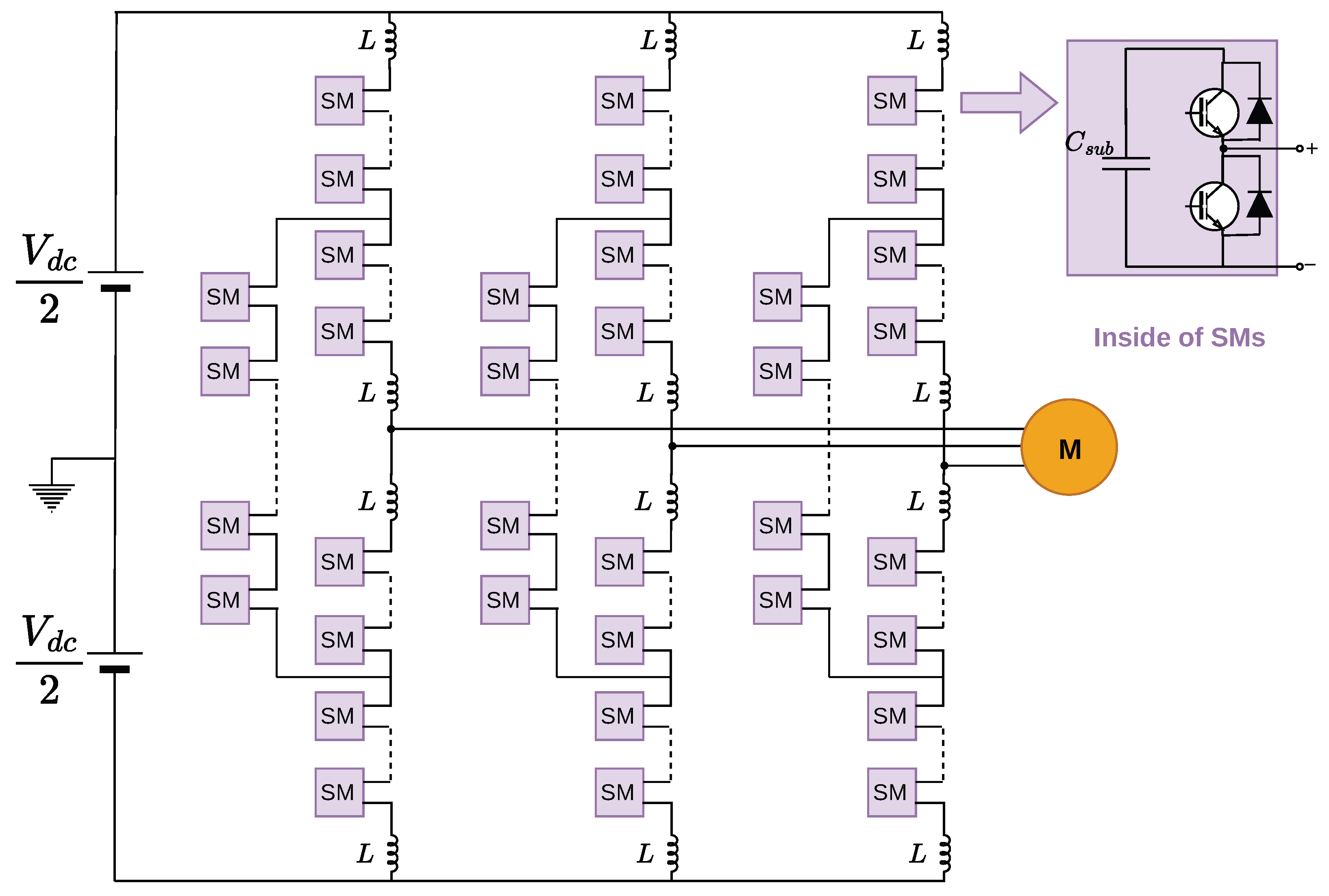
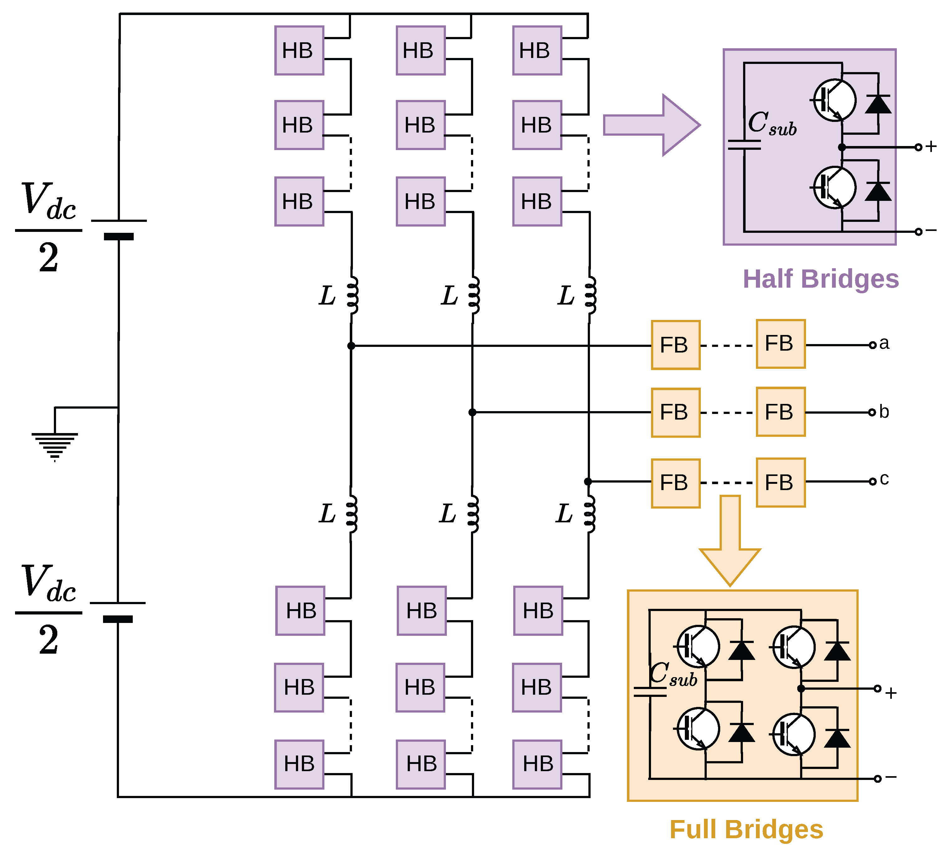
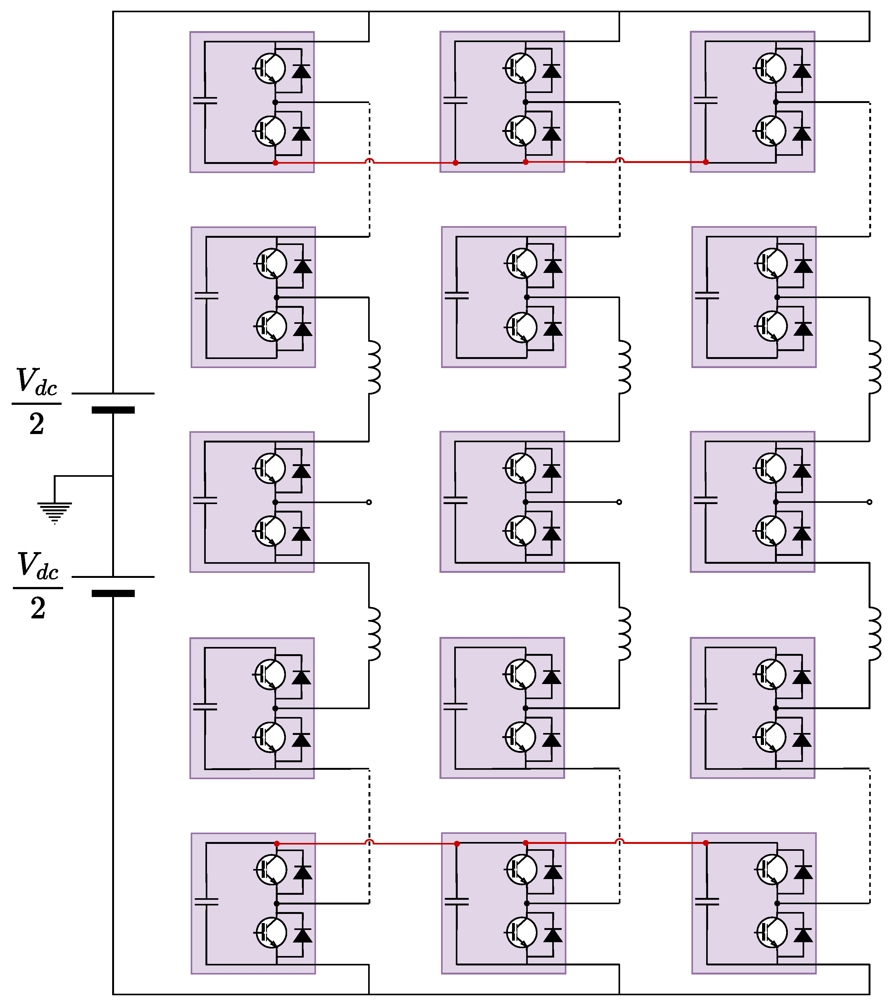
In this section, the proposed A–E classification is applied to DC–AC MMCs (motor-drive and grid-interface operation), where the dominant low-frequency SM capacitor-voltage ripple is primarily linked to the arm-energy oscillation at the fundamental and its second harmonic components. The methods are grouped according to the physical mechanism by which the ripple power is processed and the additional hardware pathway introduced to redistribute, buffer, or decouple that energy. Group A covers approaches that create explicit physical power channels, typically via high-frequency magnetic links, to transfer ripple power between arms or phases. Group B includes transformerless and topology-level auxiliary channels (e.g., middle-cell or active bridging structures) that shape the internal energy exchange without galvanic isolation. Group C comprises hybrid and reconfigurable MMC variants that exploit additional switching states or mixed submodule types to manage arm-energy imbalance under low-speed conditions. Group D collects methods that employ dedicated energy-storage interfaces to buffer ripple energy, while Group E captures architectural and design-oriented solutions (e.g., structural modifications and selection guidelines) that mitigate ripple through system-level reallocation of stored energy and practical design trade-offs. In the following subsections, these groups are compared not only in terms of ripple mitigation effectiveness, but also with respect to incremental hardware burden, control complexity, and impact–cost considerations.
4.1. Group A: Physical Power Channels (HF Magnetic Path)
The addition of physical power components typically results in significant suppression of the ripple while maintaining stability at low speeds [
17,
54,
64]. The trade-off is increased hardware complexity and cost due to the need for high-frequency transformers and additional power bridges, as well as the need for EMI-aware layout in the design. The approach has been implemented in several variants such as DAB- or three-port-based links, inter-phase high-frequency power-sharing channels, and wireless high-frequency magnetic coupling [
17,
54,
65,
66].
Topologies that transmit low-frequency ripple power at
or
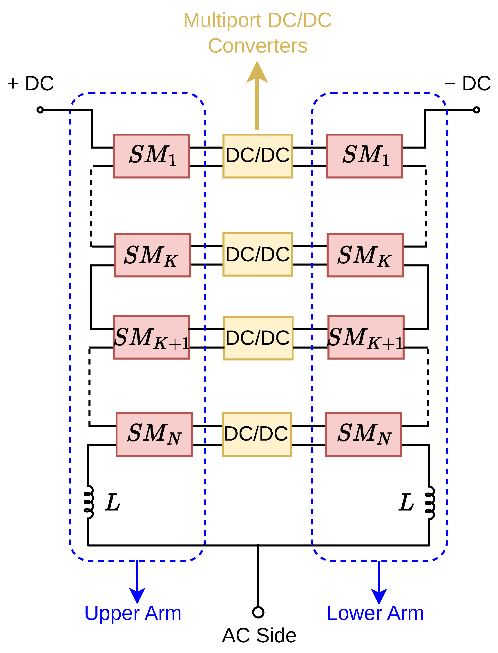
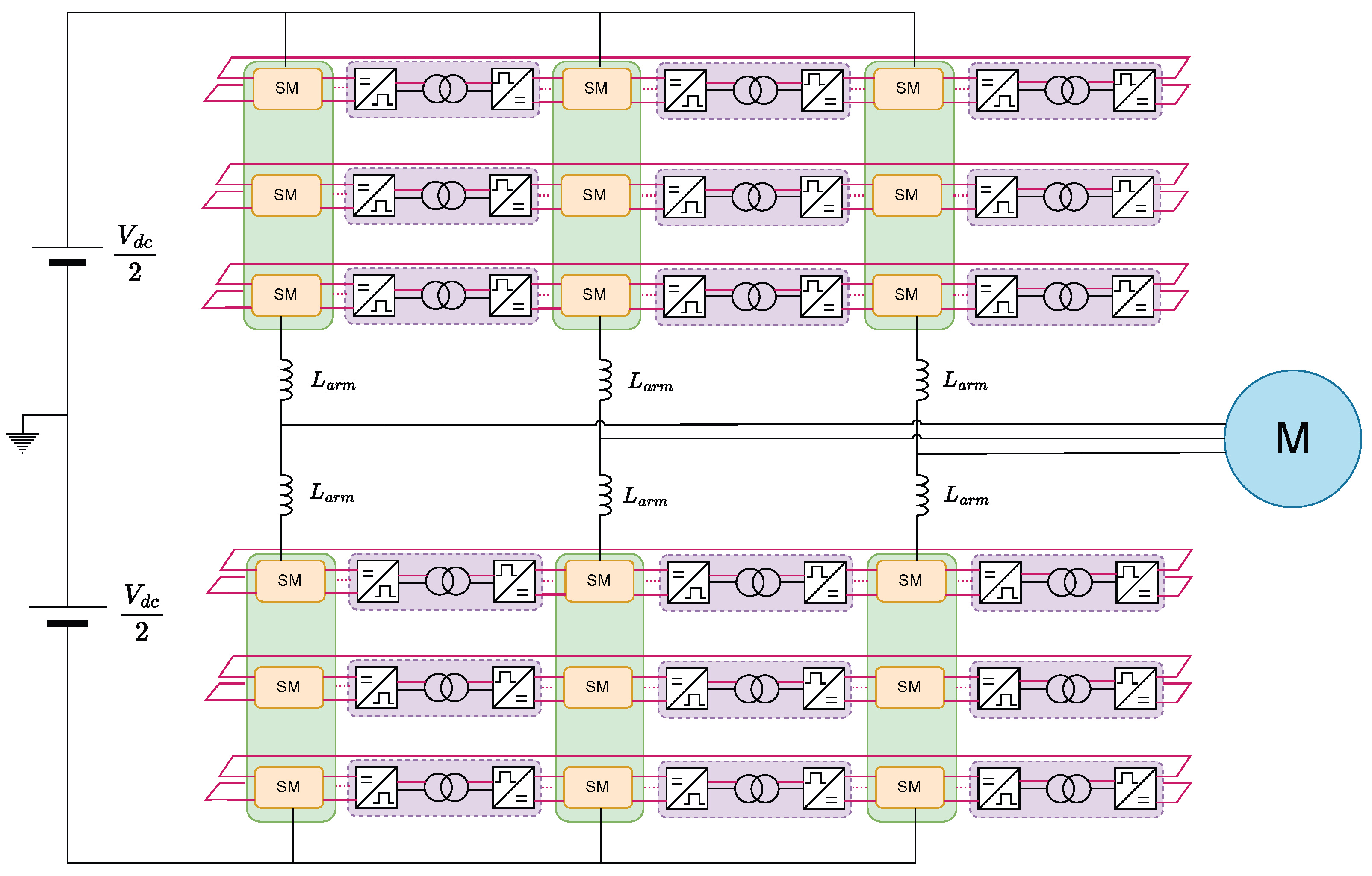
via high-frequency magnetic couplings operate on the same principle: the SMs of neighbouring arms at the same level are laterally connected via HF transformer-based DHB/DAB intermediate converters, and ripple power is compensated instantaneously between phases. In [
17], DHB converter based ripple-power decoupling channels established between the three phases simultaneously separate the Differential-Mode (DM) and Common-Mode (CM) components as illustrated in
Figure 4. Thus, the SM capacitor voltage ripple is substantially reduced while maintaining full torque at low speed.
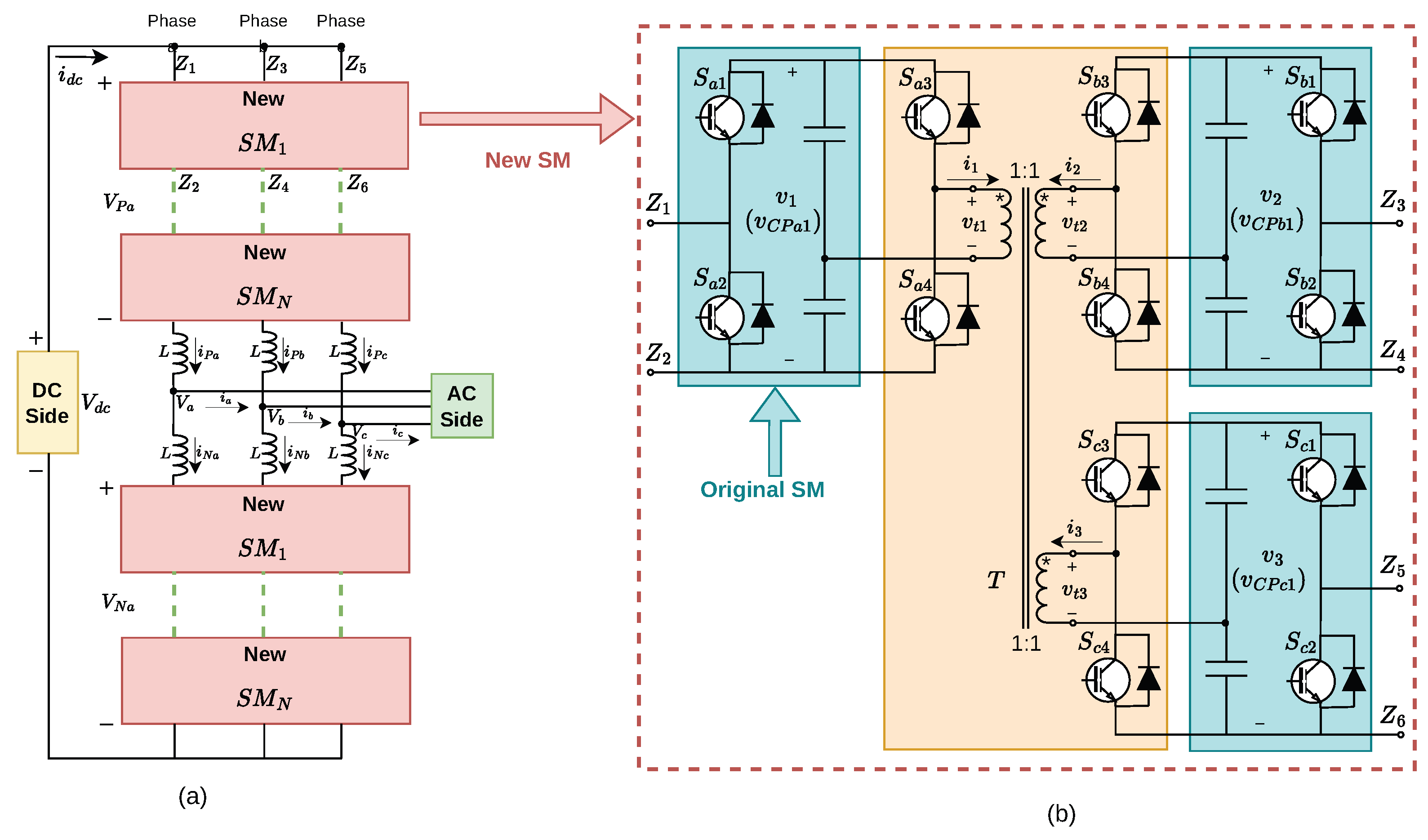
In [
67], the MMC-PET hybrid, the
circulating current injection on the MMC side suppresses CVR, while the DAB phase shift transfers the fundamental ripple power to the HF link; the architecture is summarised in
Figure 5—‘Upper-lower arm coupled MMC–PET’.
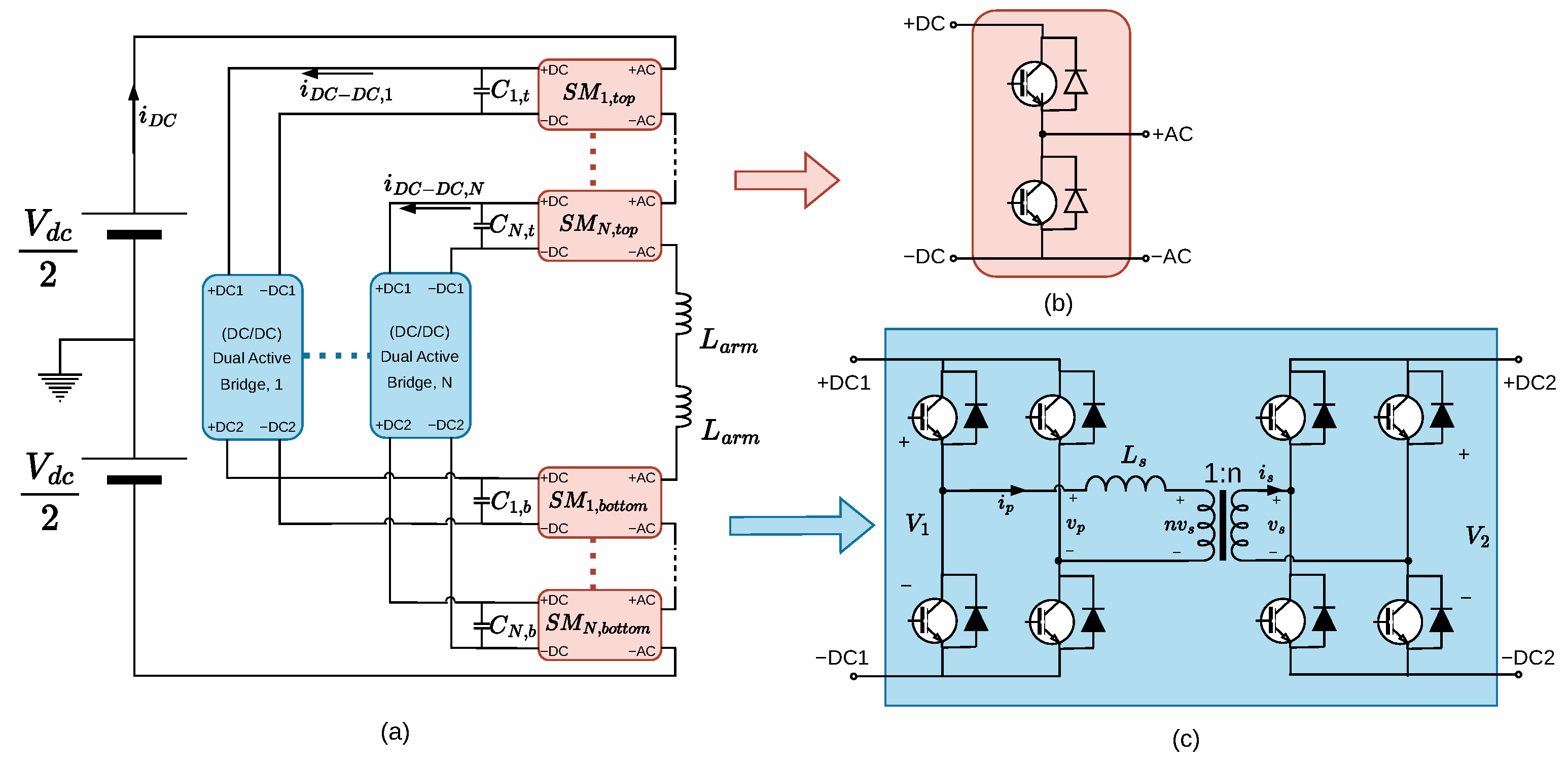
In [
54], an intra-arm variant is implemented in Arm-Link Enhanced (ALE) MMC as shown in
Figure 6. The upper and lower arm SMs are connected via a DAB. Since the DAB current depends solely on the arm modulation, SM voltage measurement and sequencing are not required, the capacitor is reduced, and the DAB operates continuously in Zero-Voltage Switching (ZVS).
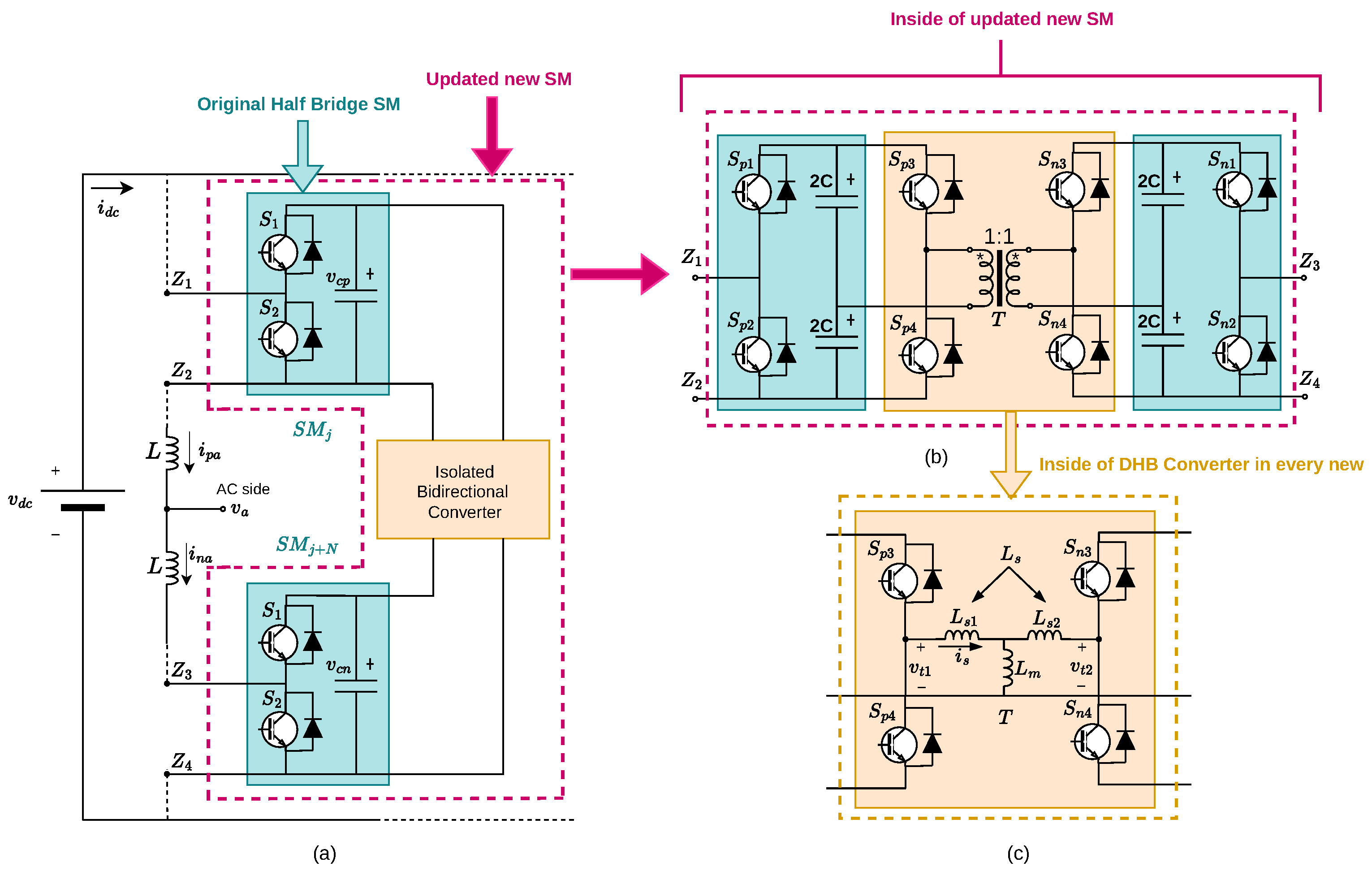
Similar to ALE-MMC [
54], an isolated DHB-based link [
68] is inserted between each pair of SMs in the upper and lower arm, as indicated in
Figure 7. The fundamental component of the power is transferred to the opposite arm with phase-shifted control, reducing current stress and
without requiring HF common-mode injection. Briefly [
17], the DM and CM components are jointly separated using the inter-phase DHB chain as shown in
Figure 4; [
54] uses DAB between the upper and lower arms of the same phase to enable intra-arm power transfer without SM voltage measurement (
Figure 6); reference [
68] proposes a DHB power link between the upper and lower arm pair, specifically carrying the fundamental
DM component, as shown in
Figure 7; reference [
65] brings the three phases together in a three-port connection and uses the principle that the sum of the instantaneous powers is 0 to naturally cancel the components at
and
within the link (
Figure 8).
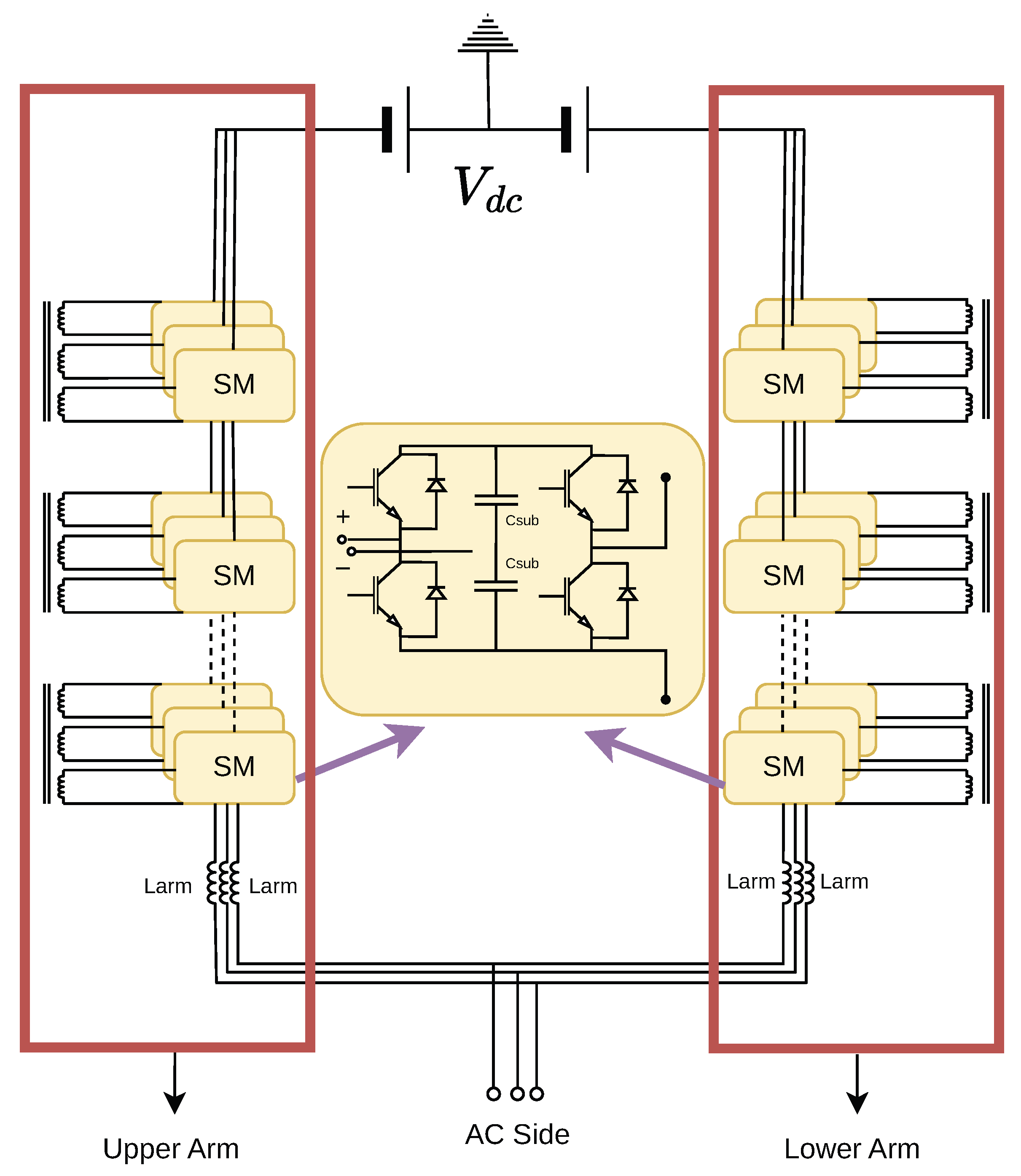
The three-port connection at the phase level is addressed in [
65]: single-phase three-winding transformers at the same level are connected laterally (
Figure 8), ensuring that the sum of the active powers are zero within the link, cancelling the components at
and
internally.
Low frequency components can also be suppressed by directing the ripple current through isolated HF channels to the target arm or phase. For example, a DHB chain placed between the phases simultaneously separates differential and common-mode components [
17]. In ALE-MMC, the opposing ripple SMs in the upper and lower branches of the same phase are connected via DAB; since the DAB current depends only on the branch modulation, it does not require SM voltage measurement and provides a wide ZVS range [
54]. The fundamental
component is transferred to the opposite arm via the DHB power channel inserted between each upper–lower SM pair; this reduces current stress and the required SM capacitance without the need for HF common-mode injection [
68]. In open-end stator winding machine drives, in the Dual-MMC configuration, HF connections are not within a single MMC but between the mutual SMs of two separate MMCs; power ripple sharing occurs between converters [
69]. The reported front-to-front DHB configuration for six-phase drives indicates a fluctuation reduction of approximately 42–84% in the
Hz range [
70].
A different option is to export the fluctuating arm power to an external energy storage system, as in the MMC-integrated battery topology proposed in [
71]. In this approach, a dedicated battery pack belonging to a modular BESS is connected to the upper and lower arms of each phase leg through an isolated three-port DC–DC converter. By actively exchanging power between the two arms and the battery, the arm powers are balanced, the fundamental circulating current is cancelled, and the three-port converter processes the fundamental power oscillation as a controlled power channel. As a result, the required arm capacitance
can be reduced even at low speeds while maintaining a narrow SM-CVR; the average power-flow duty ratio
D and the oscillation phase shift
are controlled independently.
Coupling SMs of the same level with a lateral HF connection is also an effective strategy. In the switched-capacitor HF-link (SC-HFL) MMC, this lateral link is realised by a switched-capacitor HF network across the three phases, implementing natural ripple-power decoupling without additional closed-loop control [
72].
Resonant magnetic link-based approaches switch the ripple power within the link without requiring large LF storage. In the resonant push-pull converter – high-frequency Link (RP2C-HFL), the HF link behaves like a low-impedance, constant-ratio source; thanks to three-phase symmetry, fluctuating power is automatically eliminated and the
circulation disappears [
73]. At the phase level, the three-port half-bridge (THB) + three-winding HFT connection implements the flux cancellation principle
in hardware, enabling
components to circulate within the link instead of SM capacitors [
65]. Sliding-mode-based input-impedance shaping draws the remaining LF ripple into the HFT path and balances the operating point, targeting a narrow, weak-speed-dependent SM-CVR (
Figure 9 shows only the new MMC topology; the control action is detailed in [
74]). In the wireless counterpart, the THB ports of the three neighbouring SMs in each arm are magnetically coupled to the wireless three-winding HFT; using the same flux cancellation principle, the LF DM/CM components are damped within the HF link without loading the SM capacitors, reducing the need for large LF capacitors [
66].
In the battery energy storage system approach (MMC-BESS) [
71], each battery pack is interfaced to a pair of SMs (upper–lower) via an isolated three-port DC-DC, enabling ripple suppression and module-level SoH (State of Health)/SoC (State of Charge) management. At the system level, three-port interfaces can also realise a common low-voltage DC bus for energy sharing across modules, as exemplified by bidirectional three-port converter (BTPC) designs in [
64].
For comparison, Refs. [
17,
54,
65,
68,
71,
73] mostly redistribute only ripple power within a single MMC using local HF channels; they do not provide a system-wide common energy pool and do not enable centralised control of power flow separated by duty ratio and phase shift (D–
). Therefore, local HF-channel topologies do not provide a high-level, centralised power distribution infrastructure; instead, power flow is largely a local and passive redistribution with only limited adjustments.
Table 3 comprehensively compares the practical applicability of active power decoupling/balancing units for reducing low-frequency submodule capacitor-voltage ripple (CVR) in MMCs, considering scale (simulation/experiment), power–voltage level, current stress, switching frequency, capacitance requirement, and link-design axes reported in the literature. In this context, proposed topologies for high-power MV drive scales (e.g., MW–kV range) are presented alongside applications validated through experimental prototypes at the kW level, highlighting the transition between conceptual suitability and hardware feasibility. The data show that most active decoupling channels exhibit two distinct switching layers: the MMC’s PWM carrier (typically in the kHz range) and a corresponding higher (or separate) switching frequency defined for the isolated DC–DC power channel (e.g., DHB/DAB, three-port converters, or SC-HFL networks). This separation enables low-frequency ripple power to be routed through an alternate path outside the main energy-transfer route, while also making link design (leakage inductance, conversion ratio, and magnetic-core stress) a determining engineering variable. Indeed,
Table 3 indicates that link characteristics are commonly reported via a 1:1 conversion ratio, specified leakage/auxiliary inductances, and, in some studies, multi-winding isolation transformers. The capacitance column further highlights a wide design range from mF to
F depending on the system scale and the power-decoupling architecture: while some solutions enable capacitorless/low-capacitor operation using smaller film capacitors, others indicate that a certain capacitance remains critical for buffering ripple power.
These technical parameters are more meaningful when read in conjunction with the magnitudes of CVR suppression delivered by the corresponding methods. Accordingly, the relevant performance outputs for Group A are summarised in
Table 4 as ripple-reduction percentages at the studied output frequency (
), alongside the associated hardware complexity, component set, additional cost, control complexity, and salient implementation notes. The results in
Table 4 indicate that, experimentally, suppression of approximately 66–95% can be achieved under low-speed/low-frequency conditions (1–10 Hz), whereas around 50–60 Hz most approaches report 74–90%+ suppression; with appropriate design and scaling, some HF-link-based channels can reach the order of 98–99% experimentally. In this review, the reported ripple-reduction percentages are obtained by comparing the
ripple level of the SM capacitor voltage in the conventional MMC against the
ripple level achieved after applying the proposed method at the same operating point. Here, the
ripple level refers to the peak-to-peak capacitor-voltage ripple normalised to the nominal SM capacitor voltage
. Typically,
for an arm with
N submodules. Accordingly, reported ripple levels are presented in a scale-independent form, enabling a consistent comparison across studies operating at different DC-link voltages and prototype ratings.
The reported values are typically expressed as the conv→prop improvement defined in Equation (
1), whereby the reduction in ripple magnitude associated with transitioning from the conventional to the proposed configuration is quantified in a consistent manner. The same definition has been adopted for the ripple-reduction figures reported in the tables for the other groups, where ripple levels are available. Furthermore, in studies where the outcome is reported indirectly (e.g., via capacitance reduction rather than
or % ripple), cases are observed in which an experimental ripple reduction of ∼
is reported alongside a capacitance reduction reaching up to 99.7%, indicating that different metrics can reflect the same physical goal (CVR reduction) from different perspectives.
4.2. Group B: Active Channel (Transformerless, Mid-Cell, etc.)
A second group of methods for reducing SM capacitor ripple aims at bringing the common-mode voltage (CMV) close to zero by redistributing arm power via the middle cell. This preserves the achievable torque at low frequency and down to 0 Hz. Also, reduction of CMV significantly decreases bearing current and EMI risk. This group necessitates additional semiconductor elements in the architecture, protection, and high-level control coordination.
Group B methods reduce voltage fluctuations across SM capacitors by redistributing low-frequency power fluctuations (at frequencies
and
between arms and phases using transformerless active bridges. In cross/midpoint/star-based configurations, bridging the upper–lower arms or phase midpoints with transformerless active channels is fundamental. Active cross-connected MMC, as shown in
Figure 10, eliminates the upper–lower arm power imbalance within a phase by circulating a HF square-wave current through the active cross-arm formed by series-connected HB-SMs [
55].
Similarly, Star-Channel (StCh-MMC) (in
Figure 11) enables inter-phase power sharing through star-channel branches and does not require CMV injection [
15].
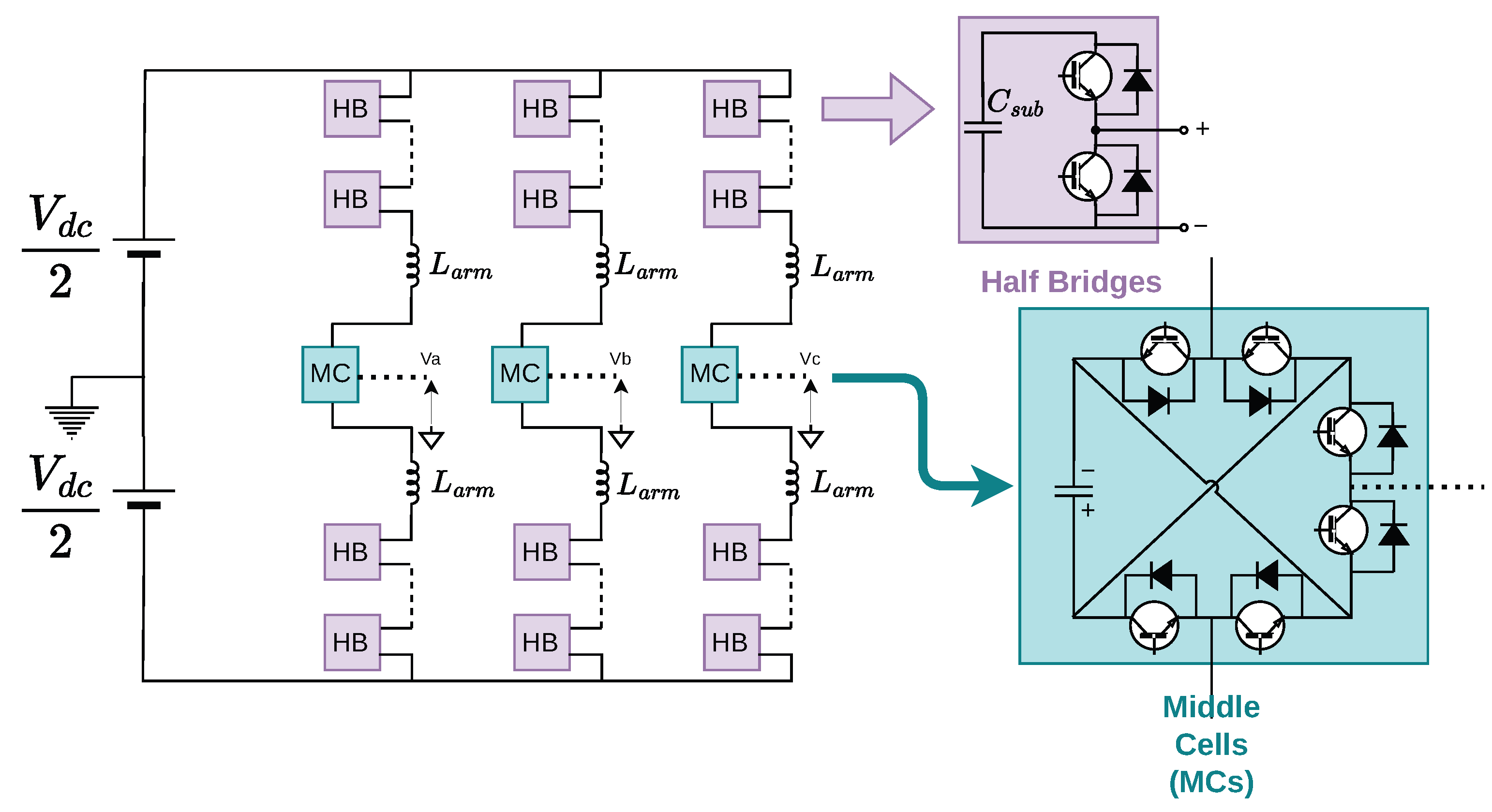
The middle-cell approach (MC, see
Figure 12) [
75] establishes an additional power exchange path between the upper arm, lower arm, and AC terminals via a three-terminal intermediate cell. The modified middle-cell structure in [
76] specifically reduces the
component via a load-connected middle circuit. In the transformerless HF power-channel topology with a centre cell [
77] the load is connected through the centre circuit; even while balancing arm powers with high-frequency switching-based power flow, the number of components is reduced compared to other centre-cell derivatives. The distinguishing feature of this subset is that the “direct” (non-isolated) bridges established at the phase level reduce both ripple and CMV in most structures.
Instead of using phase- or arm-level bridges, SM-level topologies rely on switching channels established between the upper and lower SM pairs at the same level. With the bidirectional-switching channel (BSC) [
78], the SM capacitor is connected alternately to one of two branches. Because the half-cycles of the oppositely signalled branch currents are distributed to the same capacitor, the fundamental-frequency ripple is reduced. The reversed-PWM (rPWM) channel together with a clamp capacitor
[
79] directly damps the oppositely phased capacitor ripples in the channel; the reported results show an ≈78% ripple reduction and a decrease of the total capacitance requirement to ≈12% of its original value. In this subgroup, no energy is exchanged with external magnetic components; capacitor energy is balanced locally via charge sharing and reconnection.
Arm-level midpoint schemes [
15,
55,
75,
76,
77] redirect the low-frequency (LF) power imbalance via active bridging at the arm level, thereby reducing SM capacitor-voltage ripple and often the common-mode voltage (CMV), whereas SM-level switching-channel schemes [
78,
79] attenuate the fundamental-frequency (
) ripple component by enabling local charge transfer between the corresponding upper- and lower-arm SM capacitors, with further improvement when a clamp capacitor
is added. Neither approach requires an isolated high-frequency transformer (HFT), resulting in simpler hardware. However, control and protection requirements demand careful attention. The differences and their practical implications are summarised in
Table 5, noting ripple reduction, hardware, control complexity, and additional cost.
4.3. Group C: Hybrid-MMC (DC-Bus Series Switch, HB + FB and DC-Link Management)
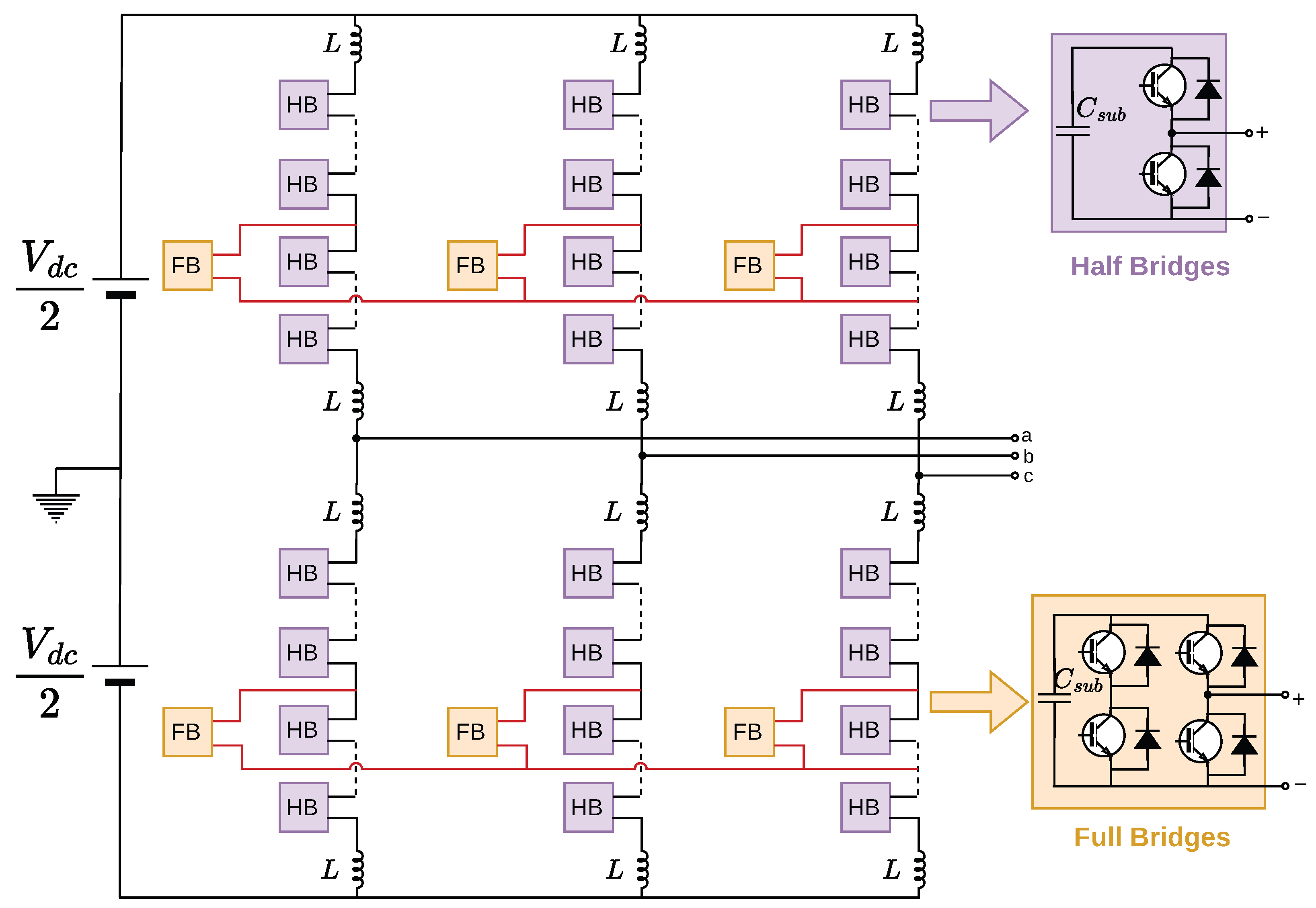
Group C aims to reduce SM capacitor-voltage ripple by reshaping the submodule energy profile in hybrid MMC topologies using a mix of HB + FB submodules, DC-series switches, or variable DC-bus configurations; some variants also reduce CMV. These schemes can achieve significant CVR reduction without substantial additional hardware and can lower the required capacitance by exploiting the additional degrees of freedom introduced by the hybrid cells (such as extra switching states and insertion possibilities) to shape internal energy exchange and attenuate the dominant low-frequency energy oscillation. However, the available timing margins and feasible operating windows can be relatively narrow and more sensitive to modulation errors and parameter variations; as a result, DC-fault behaviour and protection coordination become more complex and typically require explicit definition of fault-detection criteria, blocking and restart sequences, energy dissipation paths, and semiconductor ratings.
One approach to reducing CVR at low frequencies is to shape the DC-link voltage so that the average (DC) component of the arm voltages is reduced; this, in turn, attenuates the dominant arm-energy oscillation at the fundamental frequency
under low-speed operation. In [
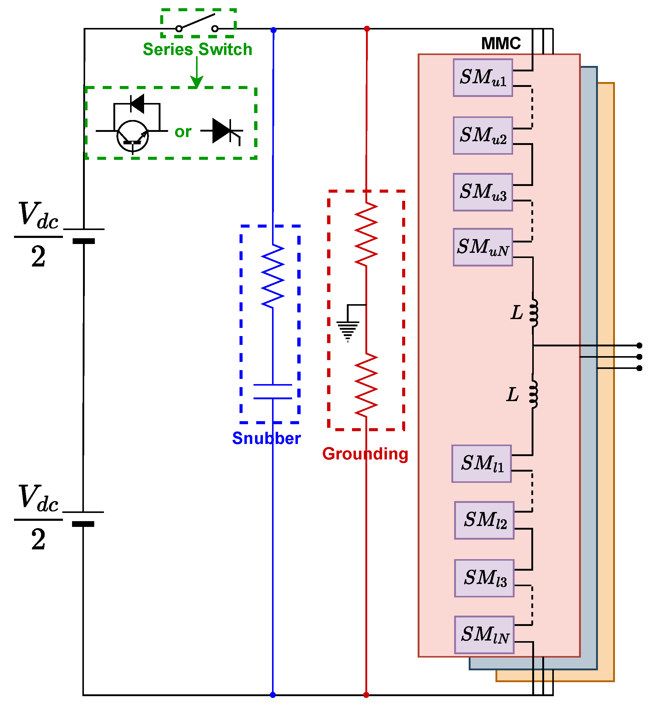
1], a series switch is placed between the DC source and the MMC; high-frequency on-off operation or the switch lowers the average DC level ‘seen’ by the converter, and the SM energy oscillation is significantly reduced (see
Figure 13—‘Traditional MMC with DC-link series switch’). Furthermore, ref. [
80] deliberately lowers the average capacitor voltage of the SM in the series switch hybrid MMC, thereby increasing the relative CVR tolerance for the same absolute ripple.
Reference [
81] combines this approach with lateral HF coupling: while the series switch reduces the average arm voltage, the added HFT/HFL interconnection provides a high-frequency magnetic link so that a large portion of the SM fluctuation current is diverted into the coupling path (where the three-phase components cancel by superposition) rather than flowing into the SM capacitors. The arm-interchange approach in [
82] converts the DC-bus to a square wave at a specific interchange frequency using an integrated gate-commutated thyristor (IGCT)-based H-bridge at the front; energy exchange between arms is performed using the negative, zero, and positive states of the FB-SM-MMC at the rear, keeping CVR balanced down to 0 Hz. In [
83], the input 12/24-pulse rectifier is reconfigured as a function of speed; thus, the observed average DC level scales with operation and CVR decreases without injecting circulating current.
The second approach is to reshape the energy profile with hybrid phase-leg architectures using modulation and the negative-voltage capability provided by the hybrid submodules. In [
84], a mix of HB-SMs and FB-SMs increases the modulation index with third harmonic voltage injection and suppresses the power ripple at
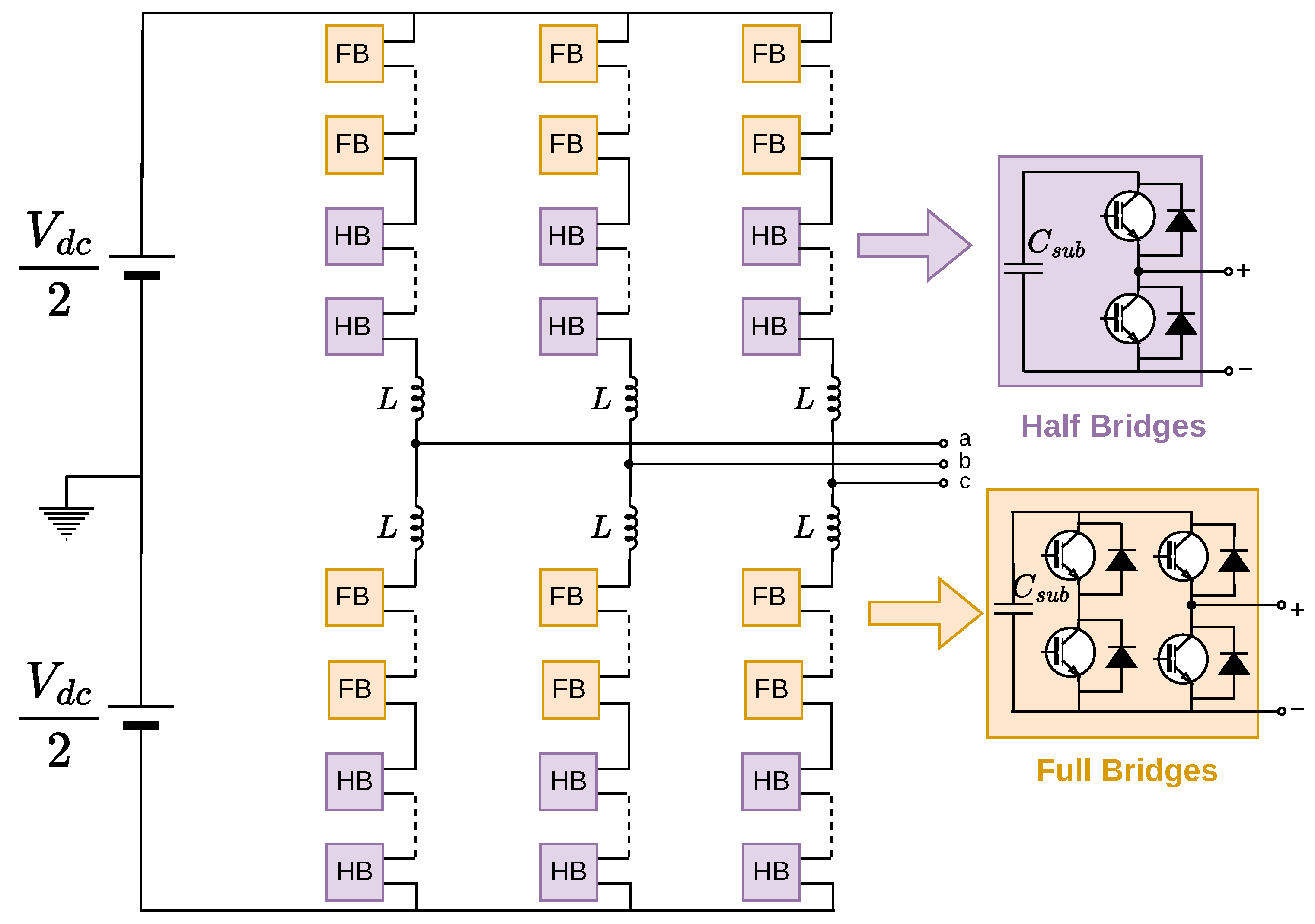
with second-harmonic circulating-current injection (SCCI); the total capacitance decreases to ≈50% of the value required without the hybrid phase-leg. A typical layout of the mixed HB + FB arrangement is shown in
Figure 14. In [
85], the
state of selected FB-SMs and selection and sorting algorithms limit the SM energy oscillation. The authors of [
86] have analytically derived the
relationship under overmodulation conditions and provided the optimal
m.
Reference [
87] creates an asymmetric hybrid phase-leg using FB wave-shaping cell (WSC) + direction switch (DS) in two phases and HB-WSC in the third phase; thanks to the half-period time-sharing of the DSs and the branch voltage wave-shaping of the WSCs, the low-frequency component of the branch power is redistributed and the peak-to-peak value
of the SM energy oscillation is reduced. As a result, the required total capacitance and arm inductance can be reduced; DC fault blocking capability is maintained thanks to the presence of the FB path. Furthermore, ‘Hybrid MMC using FB-SMs on the AC side’, as indicated in
Figure 15, represents the approach that reduces CVR by redistributing the arm power spectrum at high frequency with FB-SMs added on the AC side that inject high-frequency power [
88].
A third approach is to attenuate ripple at its source through storage/PET integration. In the MMC-integrated composite energy storage (ICES) concept, batteries and supercapacitors are integrated into different phase arms of the MMC via DC–DC converters; low-frequency SM capacitor-voltage ripple can be suppressed under low-speed, high-torque operating conditions, the MV dc bus is regulated by a dedicated dc-link voltage control loop, and the impact of pulsed loads on the integrated power system (IPS) is mitigated [
89]. In the mid-cell ‘modified MMC’ structure, the third-harmonic voltage injection selective (THVI)/harmonic current injection (SHCI) combination provides independent power degrees of freedom in the arm powers, enabling elimination of the dominant fundamental component and thereby reducing SM capacitor-voltage ripple; the mid-cell actively compensates for the CMV that THVI may generate [
90]. Reference [
91] presents an integrated MMC-power flow controller (PFC) approach for traction systems with asymmetric energy storage: batteries and supercapacitors are connected asymmetrically between upper and lower arms; power factor (PF) and voltage imbalance partial compensation is performed with hierarchical control and circulating-current suppression control (CCSC), branch currents and CVR decrease; HIL tests report RMS current
, CVR
, and field data report
operational cost savings.
Those managing the DC-link and energy storage [
1,
80,
83,
89] (and in hybrid form [
81]): the average DC level and power flow scales according to operating conditions via a series DC switch with step-down rectifier or integrated composite storage with bidirectional DC-DC; basic DC energy components are reduced → SM-CVR decreases even at low (near-0-Hz) frequencies. In MVDC IPS, it regulates the busbar with decoupled control and mitigates the pulsed load effect [
89].
HB + FB hybrid phase-legs [
84,
85,
86,
87]: reshape the energy profile with negative voltage conditions, over-modulation, and selective
circulating-current injection degrees of freedom; Ref. [
88] adjusts the arm power spectrum without distorting the output waveform, reducing CVR and CMV; arm-interchange [
82] limits LF ripple by time-sharing of the DC bus and branch state changes; mid-cell + harmonic injection [
90] reduces arm power components at source with 3rd harmonic + optimised
and compensates CMV.
The ripple reduction, hardware, control complexity, components used, and additional cost profiles of methods in this group are summarised in
Table 6.
4.4. Group D: SM-Level APD and Phase-Level APF Approaches
Group D approaches remove the low frequency power harmonics at and from the main energy path and buffer them in an APD capacitor or an external storage element by adding active power decoupling stages at the submodule level or at the phase level. These stages can be realised using distributed or semi distributed architectures, for example as DC-DC APD converters placed in each submodule or in selected submodules, or as a per phase active power filter. By diverting the low frequency ripple power away from the main submodule capacitor, the required submodule capacitance is reduced and the submodule RMS current and losses decrease. The concept remains scalable when standard submodule voltage balancing measures are applied, for example capacitor voltage sorting and selection with appropriate insertion sequencing and, when needed, arm energy balancing via circulating current or zero sequence injection. The main disadvantage is the need for additional converter stages, inductors, and control loops.
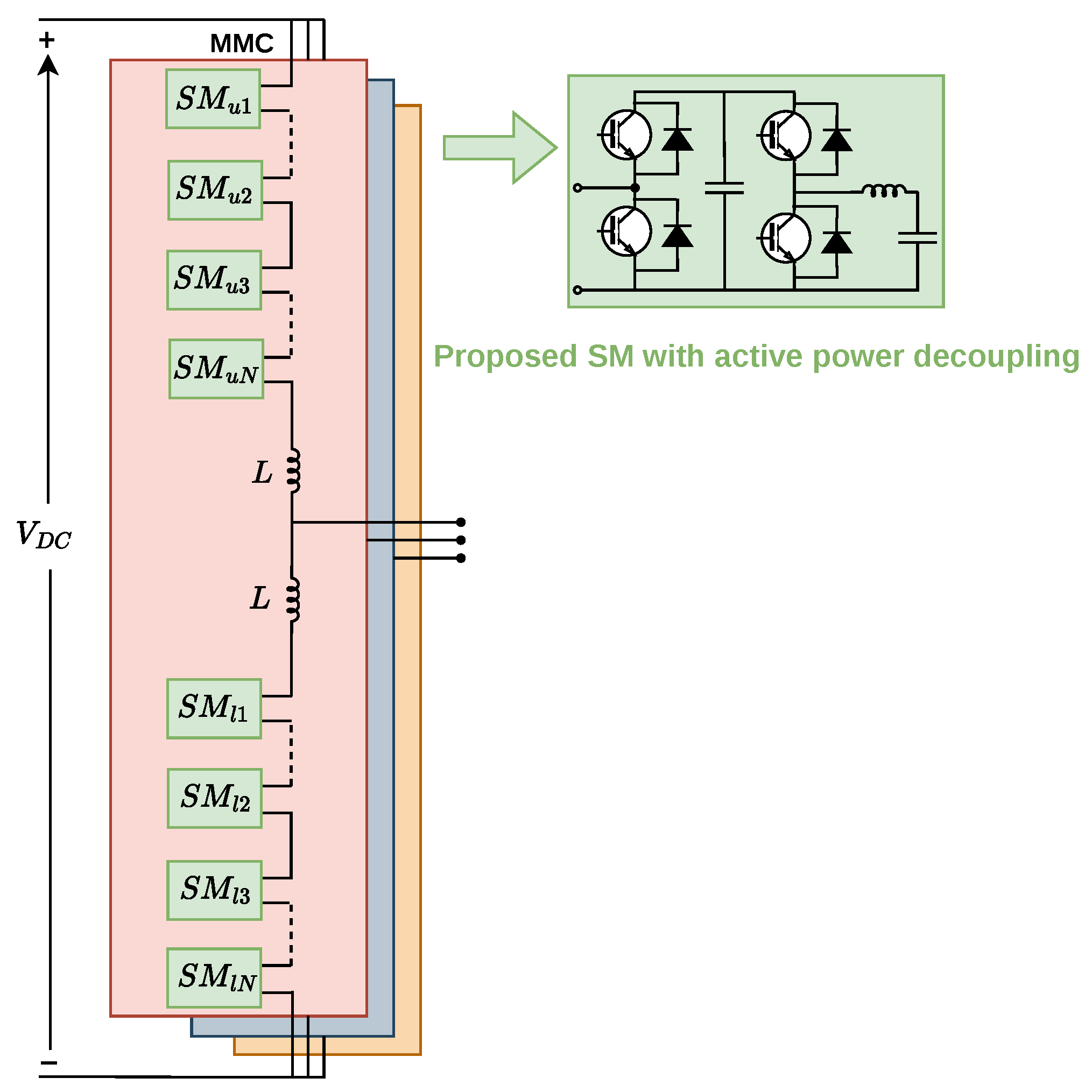
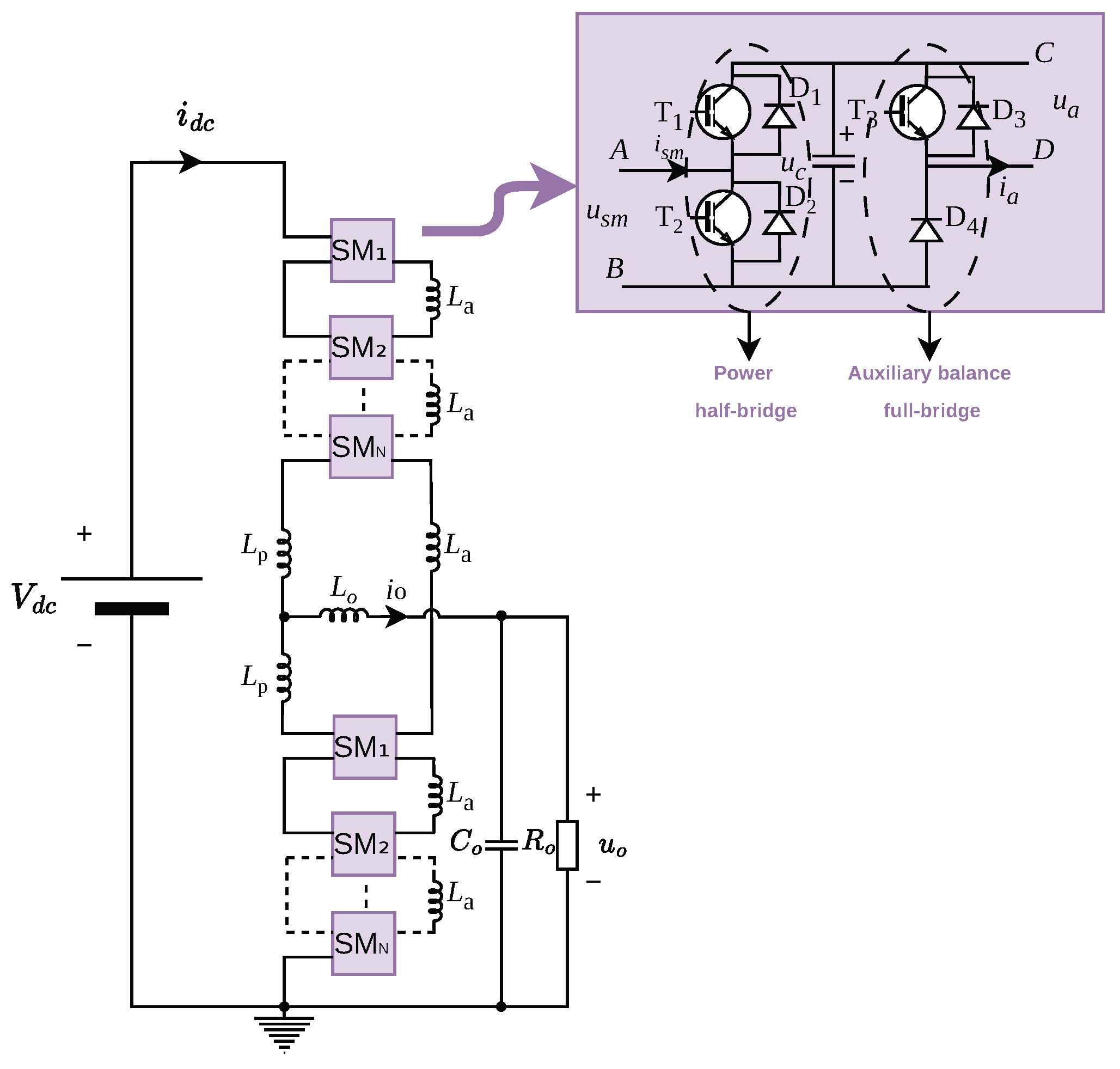
The additional converter embedded within the SM is shown in
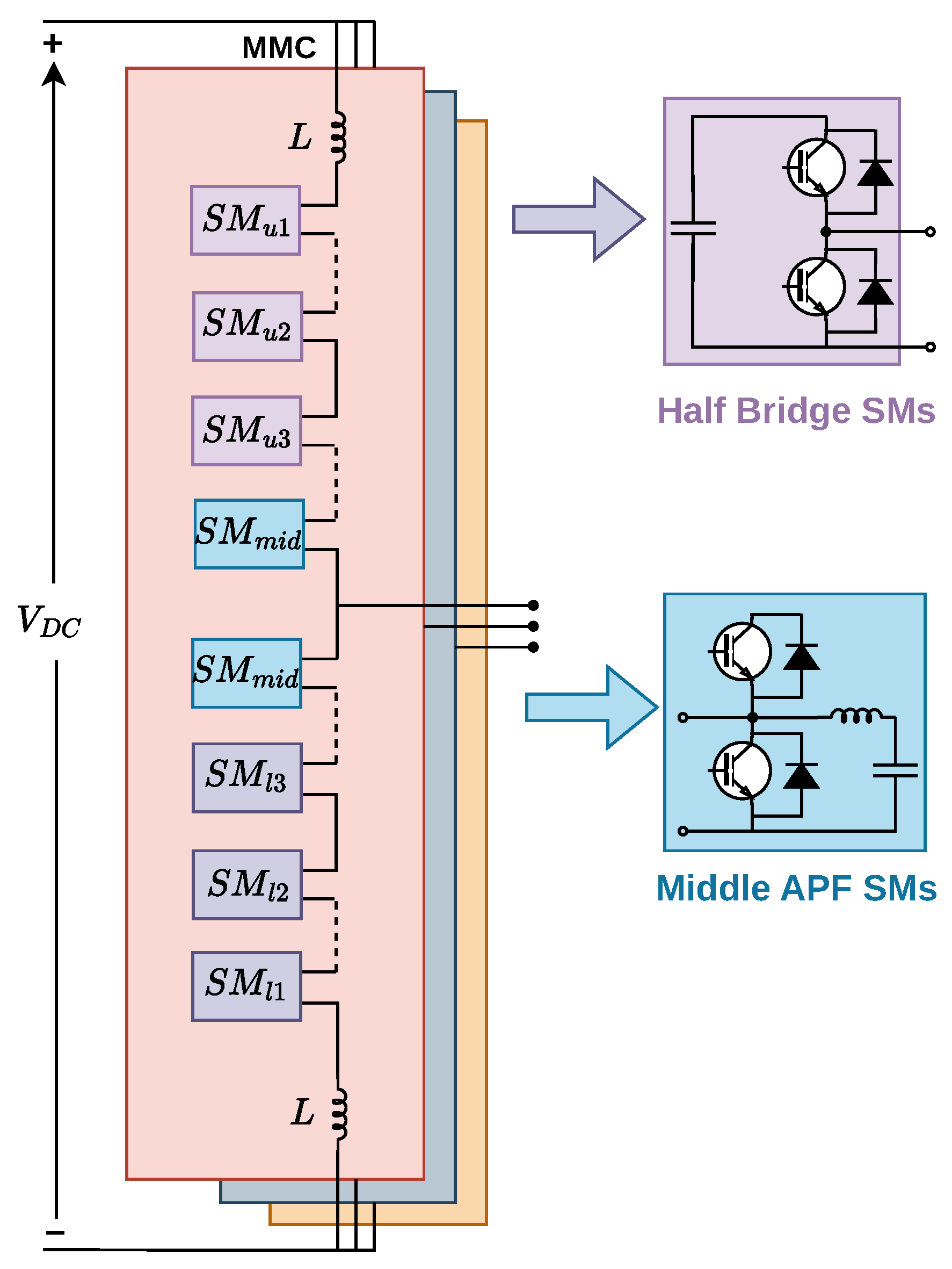
Figure 16, while the phase-level separation with an APF (Active Power Filter) arm added per each phase is shown in
Figure 17.
The component at
of the circulating current is suppressed by a closed loop [
92]. In [
93] the harmonic suppression is enhanced with PI + repetitive control without requiring HF common-mode voltage injection. The APD is implemented as an integrated APD-SM, sharing two switches with the full-bridge submodule; the APD, operating in buck and boost mode during the FB-SM’s zero-voltage switching (ZVS) intervals, transfers power to the auxiliary capacitor and reduces CVR [
94]. Within the SM-internal (cellular) APD, the representative APD-SM arrangement shown in
Figure 16 transfers the ripple power to the auxiliary capacitor within the cell via an auxiliary converter. In [
95,
96], based on a split-capacitor SM (SC-SM), the fundamental and second-harmonic components within the same SM are arranged to cancel each other, yielding an
reduction in LF ripple and a relative ripple of about
in laboratory measurements with dual-cycle control. Reference [
97] directs ripple power to an auxiliary capacitor at the cellular level by placing a buck converter in each SM without adding an out-of-phase branch; the advantage is a significant reduction of CVR, the cost is an additional switch and inductor per SM and cellular control complexity.
Figure 16.
Proposed MMC SM with active power decoupling [
93,
97].
Figure 16.
Proposed MMC SM with active power decoupling [
93,
97].
At the phase level of the APF line, as shown in
Figure 17, a buck-APF arm added to each phase collects the low-frequency ripple power in an external APF capacitor. Reference [
98] proposes an APF-MMC that achieves higher suppression of low-frequency harmonics by using two high-frequency control degrees of freedom to shift the relevant power components to a higher-frequency region; the load current remains in the main converter power path, while the APF arm provides a separate current path for the low-frequency ripple power, so ripple buffering is physically separated from the main power transfer. Reference [
99] combines a shared single mid-SM with a series buck-type APF; an additional buffer capacitor is used to handle the
ripple-power component, as the APF arm injects a compensating current that steers this component into the buffer capacitor rather than into the main SM capacitors, and an
CVR reduction is reported in simulations and experiments. In [
100], a buck-APF is placed in the
nth SM of the upper arm and the lower arm’s first SM; SM ripple
and average SM current
reduction are reported (simulations and experiments).
Figure 17.
Per-phase APF-integrated mid-SM APF-MMC topology (buck-APF in each phase) [
100].
Figure 17.
Per-phase APF-integrated mid-SM APF-MMC topology (buck-APF in each phase) [
100].
From a comparative perspective, SM-internal topologies buffer the power harmonics within each submodule and enable faster local energy balancing by providing a short internal path for ripple-power exchange, whereas phase-level topologies largely preserve the existing SM topology and add an adjustable suppression channel per phase. When compact submodule-level integration is the main objective, SM-level APD is more attractive; when retrofit flexibility and phase-wise regulation are prioritised, phase-level APF becomes more appropriate. A comparison of these findings is provided in
Table 7 (“Group D—Comparison of SM-level APF approaches”), which summarises the strengths and limitations of each method in terms of ripple reduction, hardware and control complexity, and additional cost.
Table 7.
Comparison of Group D (SM-level APD) approaches.
Table 7.
Comparison of Group D (SM-level APD) approaches.
| Method | Ripple Reduction | Hardware Complexity | Components | Additional Cost | Control Complexity | Additional Information |
|---|
| SM with APD (auxiliary HB + L + split C) [92] | 91.36% (s)/ 87.84% (e) at 50 Hz | Medium–High | Additional HB, L and C | Medium | Medium–High | Fundamental/2f power is routed through the APD path; required capacitance is reduced. |
| Intra-SM APD (bidirectional buck–boost; PI and repetitive control) [93] | 84.78% (s)/86.67% (e) at 50 Hz | Medium–High | APD converter in each SM + APD capacitor | Medium | Medium | Low-frequency ripple is transferred to the APD capacitor without injecting HF CMV; validated by HIL simulation. |
| APD-SM (integrated, sharing two switches with FB-SM) [94] | 85.08% (s)/82.03% (e) at 50 Hz | Medium | FB-SM with integrated APD | Medium | Medium | Buck and boost functionality; power buffering. |
| Split-Capacitor SM–based APD [95,96] | 80%(est.) (s) /88.7% (e) at 50 Hz | Medium | Split-capacitor SM + APD arrangement | Medium | Medium | Fundamental and 2nd harmonic are suppressed. |
| Per-SM APD (buck type) [97] | 92.00% (s) /90.74% (e) at 50 Hz | Medium–High | APD (switch + inductor) per SM + APD capacitor | Medium | Medium–High | Significant CVR reduction; per-SM control overhead. |
| APF-M3C (shared middle SM + buck-type APF) [99] | 49.59% (s)/ 22.48% (e) at 50 Hz | Medium–High | Middle SM + APF inductor/switch | Medium | Medium–High | Loss reduction; balancing and control strategies provided. |
| APF-MMC (per-phase buck APF) with two HF degrees of freedom [98] | 51.22% (s)/54.19% (e) at 10 Hz | Medium–High | APF leg + storage element | Medium | Medium–High | Fundamental power is shifted to HF; outperforms classical MMC at low speed (simulation + experiment). |
| APF-MMC (buck-APF inserted between selected upper–lower arm nodes) [100] | 23.33% (s)/ 19.51% (e) at 50 Hz | Medium–High | APF (buck) + storage capacitor | Medium | Medium–High | SM average current less than ∼; verified by simulation and experiment. |
4.5. Group E Structural/Topological Changes (SM/arm Architecture; MMC Relatives)
Group E encompasses approaches that passively reduce low-frequency power oscillations at and 2 at their source through topological revisions made at the SM and arm levels on the standard MMC architecture. Instead of adding active APF channels, the converter’s internal energy-sharing paths are rearranged so that the ripple power is spread over more capacitors; thus, becomes smoother and the capacitance required per individual SM can be reduced. The absence of an additional HF magnetic component or external power channel simplifies hardware integration; however, the topologies require a rethinking of the modulation, balancing, protection, and fault detection processes.
Parallel-C and three-level SM configurations reduce capacitor-voltage ripple (CVR) at low switching frequencies by enabling parallel connection of submodule capacitors at the intermediate level; some designs achieve a similar effect with fewer semiconductors, drivers and sensors [
101,
102]. In the diode-clamped HB-MMC group, often described as spontaneous capacitor parallel behaviors (SCPB), clamp diodes and RC damping networks, together with auxiliary networks distributed across phases produce inherent self-balancing of cell voltages, easing sensing and communication needs [
103].
As illustrated in
Figure 18, M-MMC introduces a mid-SM-assisted auxiliary coupling between the top and bottom SM capacitors, creating an internal equalisation path that reduces the fundamental and
components; suppression is strengthened with PI + R control, and a saving of one SM per phase is reported [
104]. In Dual-MMC (open-end), two MMC legs are modulated with opposite phase and adjacent arms share a submodule capacitor; hence, the number of SM capacitors is halved (with the SM count unchanged), while high torque at low and zero frequencies is maintained [
105]. Single-arm MMC (SAMMC) merges upper and lower arms into a single arm so that all capacitors are continuously engaged via four-terminal SMs; for the same voltage level and ripple target, the capacitance per SM is ≈52% and the total capacitance is ≈26% compared with a standard MMC [
106]. In
-MMSC, phase decoupling, meaning that each phase operates as an electrically independent single-phase SM string with no internal inter-phase energy-exchange path, eliminates undesired circulating currents and the need for bulky arm inductors, improving CVR under variable-speed operation, particularly at low fundamental frequencies, with an efficiency close to that of the modular multilevel matrix converter (M3C) [
107].
Within the same layer, reconfigurable topologies further reduce CVR by distributing power harmonics according to the operating conditions. With self-energy equalisation, an equalisation branch, made of a clamp IGBTs plus a limiting inductor, is added between the upper and lower arms of each leg; using appropriate switching sequences, arm energies are periodically balanced from 0 Hz to the rated frequency; no isolation transformer is needed and the additional semiconductor count is limited compared with EEM-style topologies [
108]. For the LF and HF two-mode arrangement, in LF mode only the top and bottom SMs per arm remain active while the others are bypassed; the series DC-link switch is kept open (off) and a low-voltage auxiliary source through a series diode supports start-up, achieving high starting torque and very low CVR without injecting circulating-current and CMV; as frequency rises, a designed transition to HF mode is performed [
109], suppressing fluctuations via the parallel interconnection of the top and bottom SM capacitors (accessorial cables) in LF mode.
In summary, Group E combines topologies that suppress low frequency power oscillations by revising the internal architecture of the standard MMC at SM and arm levels, without adding active power channels. SM-level parallel-capacitor and three-level, together with SCPBs reduce the ripple across
and reduce CVR by spreading ripple power across counter-phase paths within the cell [
101,
102,
103]. Arm level derivatives (M-MMC, Dual-MMC, SAMMC, 33-MMSC) regulate how fluctuating power is shared within an arm, enabling low-CVR operation in the low frequency region while reducing capacitance, sensor and inductor requirements [
104,
105,
106,
107,
108,
109]. The comparison between the topologies of this group are synthesised in
Table 8, in terms of ripple reduction, hardware complexity, component additions, incremental cost, control complexity, and additional information.




 ,
,