Article

Memristor-Controlled Reconfigurable N-path Filter Structure Design and Comparison

Institute for Integrated Micro and Nano Systems, University of Edinburgh, Edinburgh EH8 9YL, UK
*
Author to whom correspondence should be addressed.
Electronics 2025, 14(9), 1858; https://doi.org/10.3390/electronics14091858
Submission received: 30 March 2025 / Revised: 28 April 2025 / Accepted: 29 April 2025 / Published: 2 May 2025
(This article belongs to the Special Issue Advances in RF, Analog, and Mixed Signal Circuits)

Abstract

:
This paper presents the integration of memristors into N-path filter architectures to develop reconfigurable N-path filters with a tuneable bandwidth. Two different memristor-based N-path filter designs are proposed and systematically compared. One of the architectures was experimentally validated by interfacing it with a memristor package in a laboratory environment, demonstrating a tuneable bandwidth ranging from 1.5 kHz to 2 kHz at a centre frequency of 1 MHz, corresponding to a tuneable quality factor (Q factor) of between 500 and 667. Additionally, this design enables centre frequency tuning from 0.9 MHz to 1.2 MHz while maintaining a fixed Q factor of 600. The second architecture was evaluated through simulations in the Cadence Virtuoso environment using a memristor model. The results indicate a tuneable bandwidth from 0.99 MHz to 1.38 MHz at a centre frequency of 1 GHz, corresponding to a tuneable Q factor ranging from 730 to 1010. Furthermore, this design allows the centre frequency to be adjusted within the range of 0.99 GHz to 1.38 GHz while preserving a fixed Q factor of 1000. These findings highlight the potential of memristor-based N-path filters in achieving reconfigurable and high-Q filtering capabilities for RF applications.

1. Introduction

With the development of modern wireless communication technologies, reconfigurable filters are widely used in radio transceivers. These filters enable systems to adapt to different working requirements by dynamically adjusting key parameters such as the bandwidth, gain value, and centre frequency. Several different types of filter structures have been researched in designing reconfigurable filters, such as a digital filter controlled by software [1,2], Micro-Electro-Mechanical System (MEMS) filter [3,4,5], Surface Acoustic Wave (SAW) filter [6,7], Switched Capacitor filter [8,9], and so on. Of all these filter design solutions, the N-path filter structure is one of the designs which has high linearity, a high quality factor suitable for integrating on-chip and CMOS technology and a high potential for transformation [10,11,12]. An N-path filter periodically switches N identical parallel signal paths through a group of capacitors, which works similarly to the sample-and-hold operation in a sampling analog-to-digital converter. If the transfer function of one signal path forms a low-pass filter, then the periodic process transforms the low-pass filter into a bandpass function throughout the whole N-path filter [13]. A large amount of research has been conducted to design reconfigurable bandpass filters based on the original N-pass filter structure, including using a tuneable local oscillator to adjust the centre frequency of the filter and using switched capacitor or other structures to adjust the bandwidth [14,15,16,17,18,19]. These innovations aim to enhance the filter’s adaptability while maintaining performance standards at the same time.
In recent years, memristors have become novel and promising components for designing reconfigurable devices. Memristors are a type of two-terminal non-volatile electronic circuit element which can save the history of the voltage applied to them in their resistance level [20,21]. Because of this characteristic, they can be used as a programmable resistor. As the memristive device can maintain its resistance level without a power supply, its power consumption is much lower than that of other electronic elements which are volatile or active. Some research has been conducted to combine memristor crossbars with reconfigurable filters [22,23], showing the potential of these elements in adaptive circuit designing.
In this research, instead of using memristor crossbars, a novel approach which employs one or a few memristors within the basic N-path filter structure to enable bandwidth adjustment is introduced. Although the centre frequency of an N-path filter can be controlled by adjusting the digital clock, the bandwidth is fixed by the values of the resistor and capacitor; thus, the quality factor Q of an N-path filter varies when the centre frequency changes. To make the bandwidth adjustable, one memristor is used to replace the resistor in the N-path filter to generate a reconfigurable N-path filter whose bandwidth can be adjusted by the memristor resistance. By changing the memristor value, the quality factor of the filter can be maintained at a constant value in a range of the centre frequency. The range of the centre frequency in which the reconfigurable N-path filter can maintain a constant Q factor is decided by the tuneable range of the memristor.
In this paper, different methods of combining analog memristors with the basic N-path filter structure to design reconfigurable N-path filters are considered and compared. The Methodology Section first introduces the principle and function of a memristor and the function of a basic N-path filter structure, then it mainly shows two different schematics of an N-path filter combined with a memristor and discusses the functions of the N-path filter after adding the memristor. In the Results Section, first, the simulation results for the two structures of the N-path filter are compared. Then, we describe how one of the N-path filters was built on a stripboard and measured with a memristor package at a 1 MHz centre frequency in the laboratory. After that, the second N-path filter structure was simulated at a 1 GHz centre frequency. In the Discussion Section, the reconfigurable N-path filters in this work are compared with other reconfigurable N-path filter designs, the limitations of the two N-path filter structures in this research are listed, and the influence of the parasitic capacitance in the memristor on the N-path filter are discussed based on simulations of different parasitic capacitance values.

2. Materials and Methods

The purpose of this study was to combine memristors with N-path filter structures to design a reconfigurable N-path filter. To achieve this, the Methodology Section first introduces the working principles and functions of memristors (Section 2.1) and the basic structure and function of an N-path filter (Section 2.2). Then, the basic method of controlling an N-path filter by replacing its resistive elements with memristors is introduced. Following this, based on mathematical models and software simulations, this section discusses two different memristor-based reconfigurable N-path filter structures. The first (Section 2.3) uses fewer memristor elements, resulting in a simpler design, but is not suitable for higher centre frequencies. The second structure (Section 2.4) can operate at higher centre frequencies but requires more complex memristor elements, making practical operation more challenging.

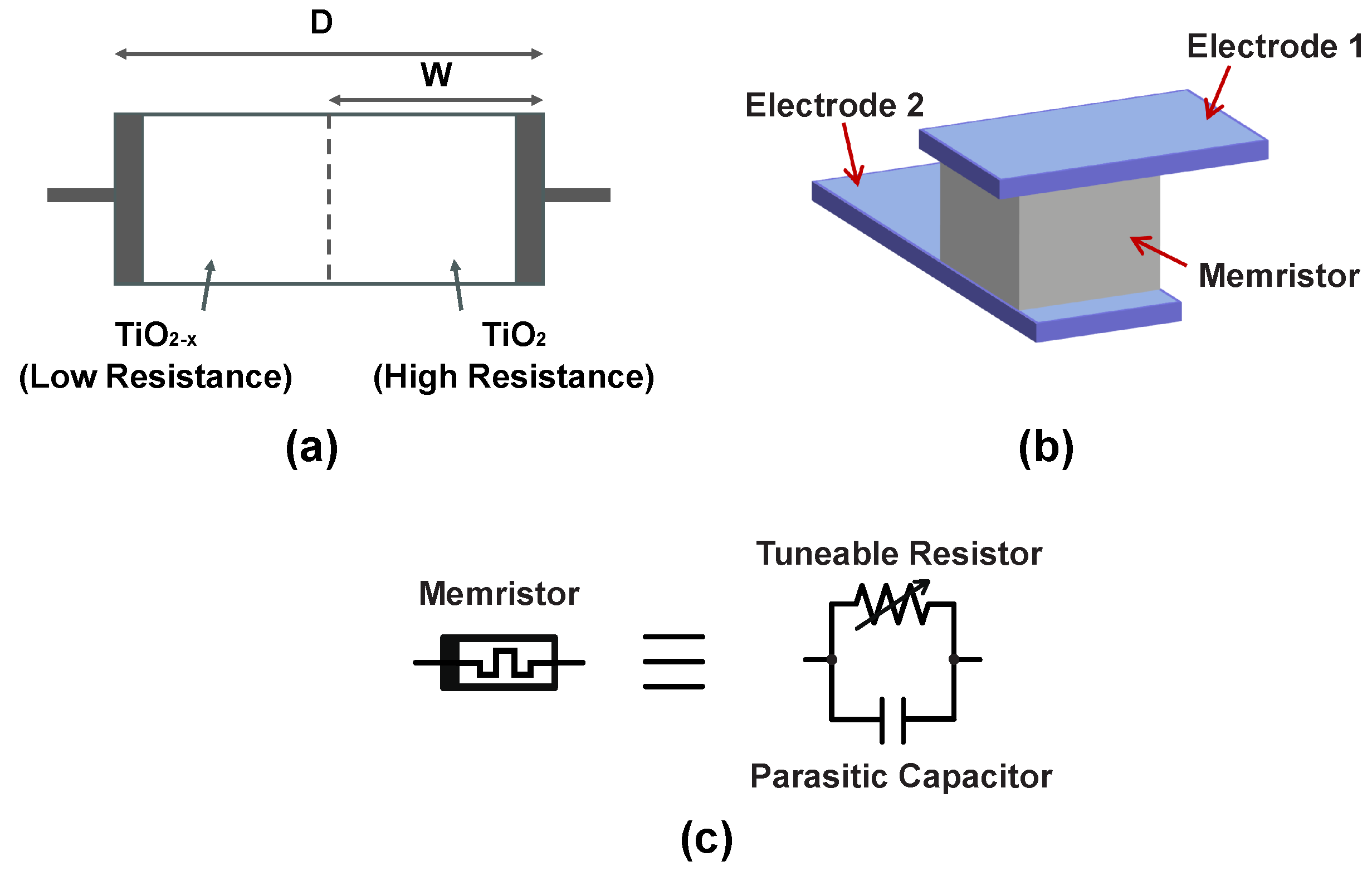
2.1. Function and Model of Memristor

Figure 1a shows the T i O 2 / T i O 2 x memristor structure produced by HP Laboratory in 2008 [21]. The memristor has a semiconductor film with a thickness of D in between two metal layers, while the letter W shows the thickness of the T i O 2 layer. The right part of the semiconductor is stoichiometric T i O 2 , in which the oxygen to titanium ratio is perfectly 2:1, and it has a large resistance. The left part of the semiconductor is also titanium dioxide but has less oxygen, which means it has a small resistance and is written as T i O 2 x . When the voltage is applied to the memristor from the T i O 2 x side, the positively charged oxygen vacancies are pushed to the T i O 2 part and transform T i O 2 into T i O 2 x . As the low-resistance region expands, the resistance of the entire memristor reduces. To make the oxygen vacancies migrate significantly through the material and change the local electrochemical structure, the voltage on the memristor needs to be greater than a threshold voltage to overcome the energy barrier. In contrast, when the voltage is applied to the T i O 2 side, the oxygen vacancies are pushed to the T i O 2 x region, and the T i O 2 region expands and increases the resistance of the memristor. The memristor reaches its maximum resistance when nearly the whole T i O 2 x layer is transformed into T i O 2 (when W = D) and reaches the minimum resistance value when all the T i O 2 molecules are transformed into T i O 2 x (when W = 0). Thus, the W/D ratio ranging from 0 to 1 can show the position of the current memristor resistance level within its whole tuneable resistance range. With further research on memristor technology, memristors of various structures and materials have now been developed [24,25,26,27,28]. However, the fundamental working principle and functionality of memristors remain similar. Figure 1b shows a 3D-model of a memristor. A memristor can be integrated at the crosspoint of two electrodes with a thin metal oxide film between them [29]. The multi-layer stack structure of memristors allows them to integrate with CMOS technologies, which also have multi-layer structures. With good compatibility with CMOS technology, a small area [30], and low power consumption [31,32], memristors have become a good choice for the design of reconfigurable devices.
A lumped element model of a memristor can be seen in Figure 1c. Ideally, a memristor should only be a tuneable resistor. However, because memristors have a metal–insulator–metal structure similar to that of MIM capacitors, a memristor also has parasitic capacitance between its two metal layers. The parasitic capacitance value is mainly decided by the area and thickness of the memristor and the dielectric constant of the insulator material, which means it will not change with the operations of the memristor. For this reason, the parasitic capacitance is assumed to be constant, and the model of a memristor becomes that of a tuneable resistor in parallel with a constant parasitic capacitance.
The memristors used in the measurements in this research were P t / T i O 2 / A l 2 O 3 / P t memristors with a 10 × 10 µm2 size [29]. The simulation model of a memristor created in the Cadence Virtuoso environment was based on the research in [33], which used a Verilog A model to simulate the function of a tuneable resistor part in the whole memristor model(tuneable resistor + parasitic capacitor). In this model, the memristor can maintain a constant resistance under 0.5 V and will show obvious resistance level variations with a voltage higher than 2 V; thus, in this research, the memristor was operated with voltage smaller than 0.5 V in the normal mode and was used with a 2.5 V voltage to adjust the resistance level in the programming mode. The model was able to accurately reproduce the voltage-dependent resistance behaviour of the memristor within the 10 k Ω to 17 k Ω range and could also provide relatively accurate results for resistance variations within the 10 k Ω to 30 k Ω range. To ensure the reliability of simulation results, the memristor resistance was constrained to within the 10 k Ω to 17 k Ω range throughout this study. The memristor was assumed to have a 10 pF parasitic capacitance in parallel in the worst case [34].

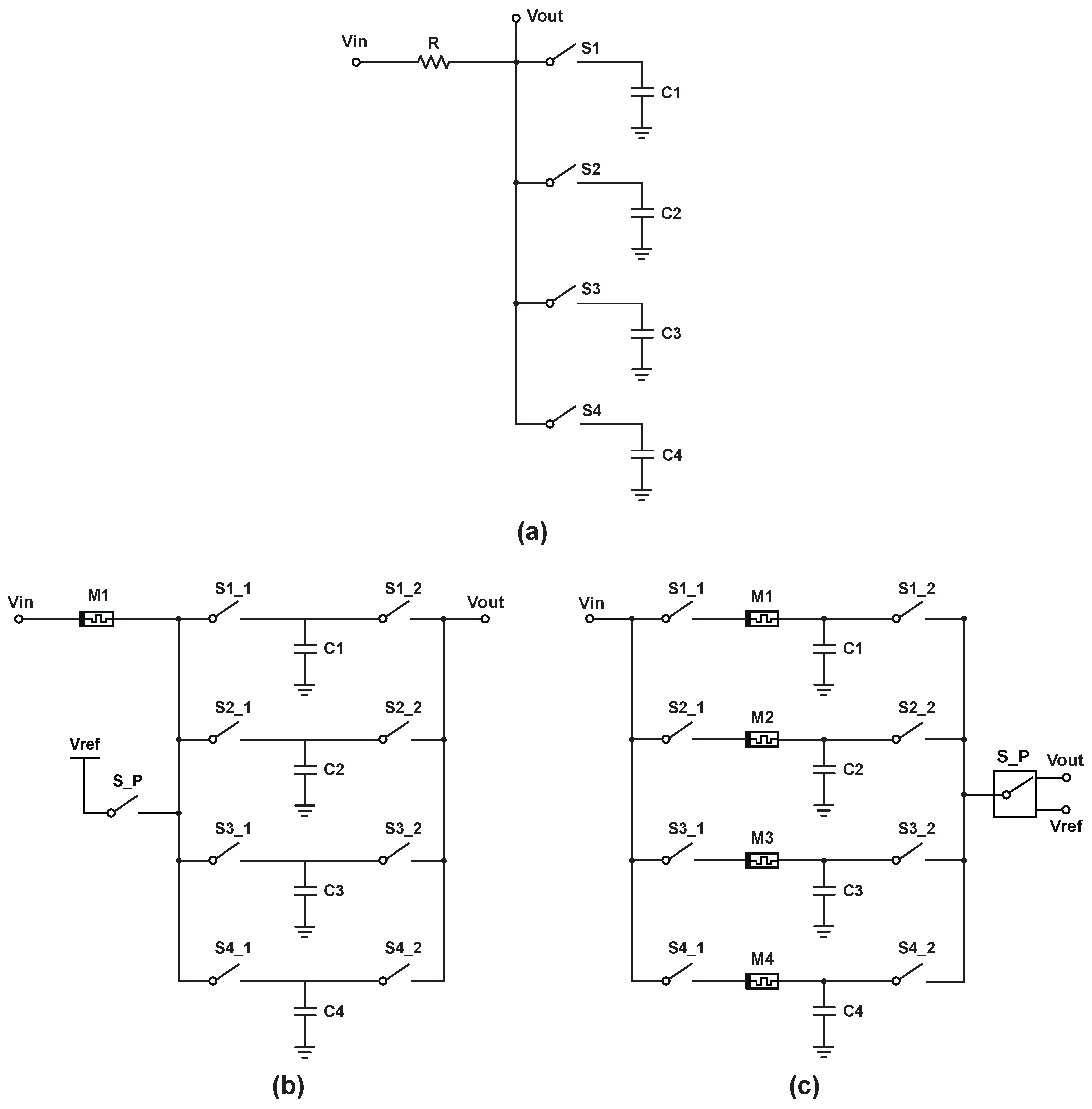
2.2. Functions of Basic N-path Filter

The basic schematic of a single-port, single-ended 4-path filter includes a resistor, R, a switch group, S1 to S4, and four capacitors, C1 to C4, with the same value C, as shown in Figure 2a. The output port is in between the resistor and the switch group [35]. Switches S1 to S4 turn on sequentially, with all the pulse widths, T o n , being the same and equal to a 1/4 of the period of the switch control signals. As only one switch turns on at any moment, the entire circuit can be considered as a low-pass filter composed of a resistor and capacitor corresponding to the activated switch.
Equation (1) shows the relationship between the resistor value (R), capacitor value (C), path number (N), and −3 dB bandwidth ( f 3 d B ) of the N-path filter [36,37,38]. The function of the quality factor Q is shown in Equation (2) and is equal to the ratio between the centre frequency ( f s ) and the −3 dB bandwidth. A benefit of an N-path filter is that the centre frequency controlled by the digital clock can be very high, which results in a very large quality factor value when combined with a small bandwidth decided by the resistor and capacitor values. By replacing the resistor with a memristor, an N-path filter becomes a basic reconfigurable filter whose bandwidth is tuneable.
Some characteristics of memristors need to be considered when combining memristors with high-frequency circuits. First, memristive devices include parasitic capacitance in their structure. For an analog memristor whose resistance can change continuously, the parasitic capacitance can be up to 10 pF [34]. The lumped element model of a memristor can be considered as a resistor in parallel with a capacitor, and the impedance of this memristor is shown in Equation (3), where R is the resistance and C p is the parasitic capacitance value. Second, a memristor shows linear I-V characteristics at a low voltage. However, when a high voltage is applied to it, the resistance level of the memristor will be changed. Therefore, the voltage across the memristor needs to be constrained to within 0.5 V during normal operation, while large voltage pulses (>1.2 V in this research) should only be applied during memristor resistance programming.
f 3 d B = 1 π N R C
Q = f s f 3 d B = π N R C f s
Assuming the switch S1 turns on, at this moment, the filter will work as a low-pass filter with a resistor, R, and capacitor, C. The function of a filter includes the ON resistance ( R o ) of the switch, which is shown as Equation (4). When the frequency is very high, the gain of the filter will tend to become a constant value which equals the ratio of R o /(R+ R o ). As R o is very small (≤500 Ω ) compared with R (≥10 k Ω in this research), the ratio is approximately equal to R o /R. Combining Equations (3) and (4), the memristor-controlled filter based on the basic N-path filter structure has the transfer function shown as Equation (5). Equation (6) expresses the condition of Equation (5) when the frequency is very high, which shows that the gain tends to 1 when the frequency approaches infinity. To generate a memristor-based reconfigurable N-path filter, some adjustments need to be made to this basic structure.
Z m = 1 1 R + s C p
H ( s ) [ + R o ] = R o + 1 s C R + R o + 1 s C = 1 1 + s R C 1 + s R o C
H ( s ) [ + M e m r i s t o r ] = 1 1 + s Z m C 1 + s R o C = 1 1 + s R C ( 1 + s R o C ) ( 1 + s R C p )
H ( s ) [ + M e m r i s t o r ] [ f ] 1 1 + 1 s R o C p 1

2.3. One-Memristor-Based N-path Filter

Figure 2b shows the modified memristor-based 4-path filter, which is called [Filter 1] in the following sections. The basic concept of the schematic in Figure 2b is a conventional N-path filter with extra switch groups [35]. In the 4-path filter architecture, 4 switches, S1_2 ∼ S4_2, are added to the circuit. The switches Sx_1 and Sx_2 are controlled with the same signal and will turn on and off simultaneously. The reason for adding extra switches is to change the location of the output ports from the point between the resistor and the switches to the right side of all the capacitors, thus reducing the influence of the switch ON resistances. Considering the schematic shown in Figure 2b, when a pair of switches, Sx_1 and Sx_2, turn on, the transfer function of the filter is shown in Equation (7), where R o u t is the load resistance of the Vout node, and similarly to in Equation (4), the model of the switches is added in the equation as the switch ON resistance R o . As the Vout is assumed to connect with the gate of the transistors, R o u t will be very large and can be considered as an open circuit. In this condition, when the parasitic capacitance of the memristor C p is very small and the frequency is not very large, the circuit transform function approximates to Equation (8), which shows that the circuit is working as a low-pass filter. In this research, the DC voltage of the input signal was set to 0.5 V to ensure that the transient voltage across the memristor would not change the memristor resistance.
H ( s ) n e w = 1 1 + s R o C + s R C 1 + s R C p × R o u t R o + R o u t 1 1 + s R o C + s R C 1 + s R C p
H ( s ) n e w [ C p 0 ] 1 1 + s ( R + R o ) C
H ( s ) n e w [ f ] 1 1 + s R o C + C C p
An additional voltage node, V r e f , is added with a switch, S_P, for memristor programming. In normal operation, V i n inputs an AC signal with an offset DC voltage of 0.5 V, S_P turns off, and V r e f is set to 0 V. In this case, ideally, the V r e f and S_P path is considered as an open circuit, and the filter works as a normal N-path filter. In the memristor programming mode, all the switches, S1_1 to S4_2, turn off, S_P turns on, and high-voltage pulses can flow between V i n and V r e f to change the resistance value of the memristor. The operations of the V i n , V r e f ports, S_P, and S1 to S4 switch groups are listed in Table 1. Programming mode 1 shows the conditions for programming the memristor from left to right, and programming mode 2 shows the condition for programming the memristor from right to left. There was no speed requirement for the memristor programming in this research; hence, the memristor programming pulse was set to have a duty of 100 μ s .
Equation (9) shows a potential drawback of Filter 1’s structure: when C p is large, the gain of the filter is no longer influenced by the resistance of the memristor but is determined by the values of R o , C, and C p . In this case, the Filter 1 circuit still cannot be used at a radio frequency.

2.4. Multiple-Memristor-Based N-path Filter

To make a memristor-based N-path filter work at a high frequency, one of the solutions is to add memristors in between each of the switch groups, as shown in Figure 2c, which is called [Filter 2] in the following sections. An N-path filter uses high-speed periodic switching to effectively downconvert the high-frequency input signal into multiple paths, where each capacitor only interacts with a near-baseband equivalent signal. However, in the Filter 1 structure, the memristor is still working with the original high-frequency signal. The impedance of the memristor reduces with increases in the signal frequency; hence, the tuneable f 3 d B range will be smaller than expected. In the configuration in Figure 2c, by placing memristors in between the [Sx_1, Sx_2] switch groups, memristors only receive a part of the signal and work in near-baseband signal environments; hence, the influence of C p is nearly eliminated.
Although the quantity of memristors that Filter 2 uses is larger than that in Filter 1, the components included in each signal path are still the same, which are one memristor, one capacitor, and the ON resistance from the switches. However, when the input signal frequency is equal to the centre frequency, in Filter 1, the memristor parasitic capacitance C p still has a large influence, while in Filter 2, the memristors are nearly working in baseband environments and the effect of C p is reduced. In this case, the frequency of the signal received by the memristors in Filter 2 corresponds to the deviation between the input frequency and the centre frequency, rather than the deviation between the input frequency and 0 Hz. The transfer function of Filter 2 is thus as shown in Equation (10), which is similar to Equation (7) but uses the deviation frequency s d instead of s. Here, s d is equal to the absolute value of deviation between the input signal frequency ω i n and the centre frequency ω s .
When programming the memristors shown in Figure 2c, the V i n and V r e f settings are the same as the conditions shown in Table 1. However, S_P becomes a single-port double-through (SPDT) switch, allowing us to choose a connection from the main circuit to the output port during normal operation, or to the V r e f port in the programming mode. In addition, differently from the programming operations in Filter 1, when programming one memristor in Filter 2, the corresponding switch groups need to be turned on, and all the other switch groups should be turned off. A potential drawback of Filter 2 is that ensuring all the memristor resistances are completely the same is hard in practical operations, which can lead to distortion in the output signal.
H ( s ) n e w 1 1 + s d R o C + s d R C 1 + s d R C p , s d = j × ω i n ω s

3. Results

In the Results Section, first the simulation results for the circuits shown in Figure 2 with resistors and memristors will be shown and compared to demonstrate the difference in the high-frequency performance of these structures. Next, we describe how a four-path filter built on a stripboard with the Filter 1 circuit structure was measured in the laboratory with a 1 MHz input signal and memristor array package. Finally, the simulation results for a memristor-based four-path filter with the Filter 2 circuit structure and a 1 GHz switch signal will be analyzed.
The switches in all the simulations had a 500 Ω ON state resistance unless otherwise specified. The memristor model used in the simulations in this research had a 10 k Ω to 17 k Ω resistance under a 0.5 V DC voltage [39] and was assumed to have a parasitic capacitance of 10 pF [34].

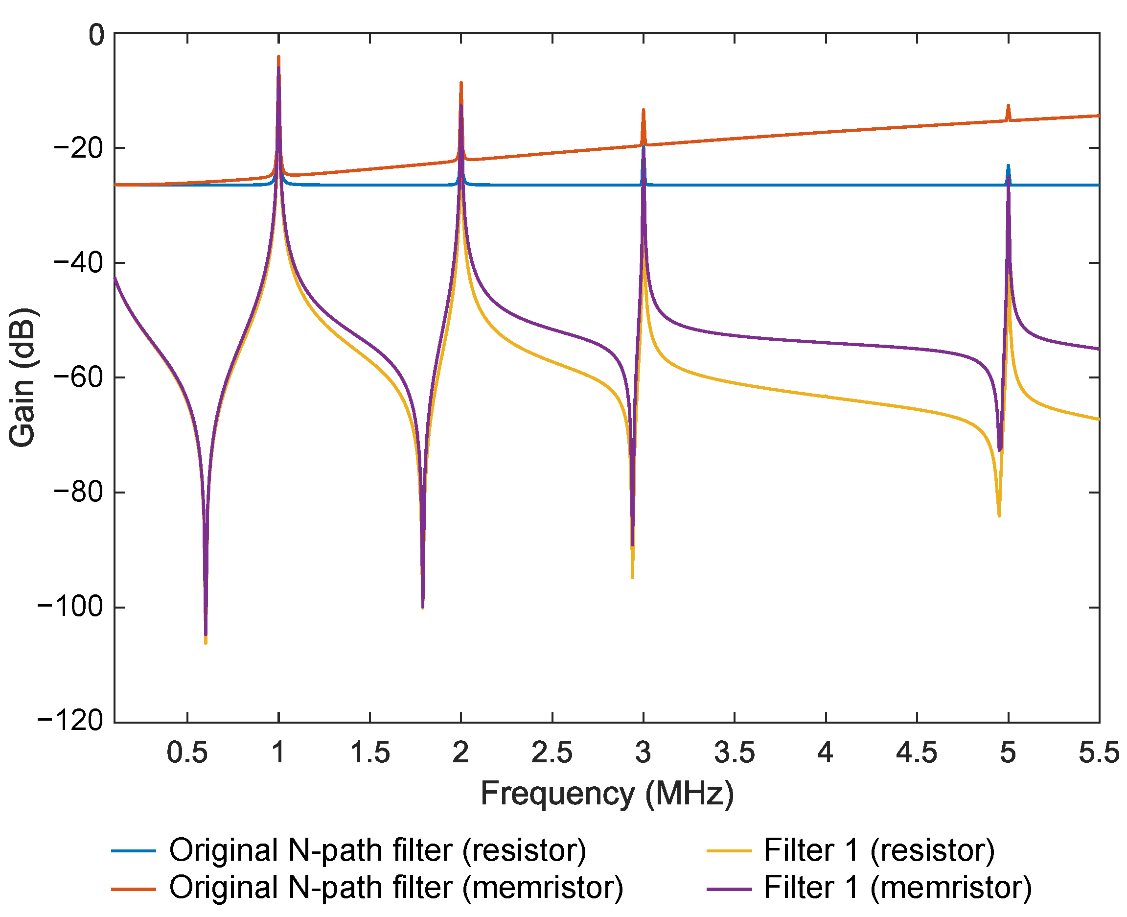
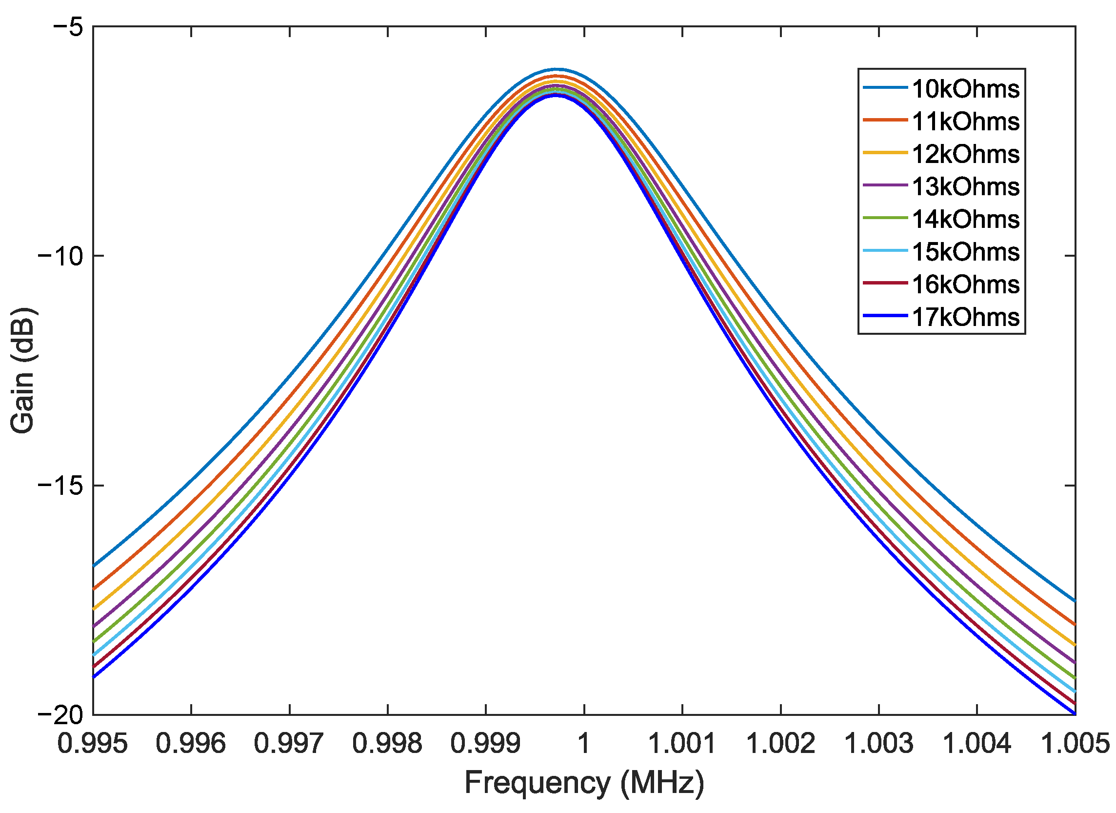
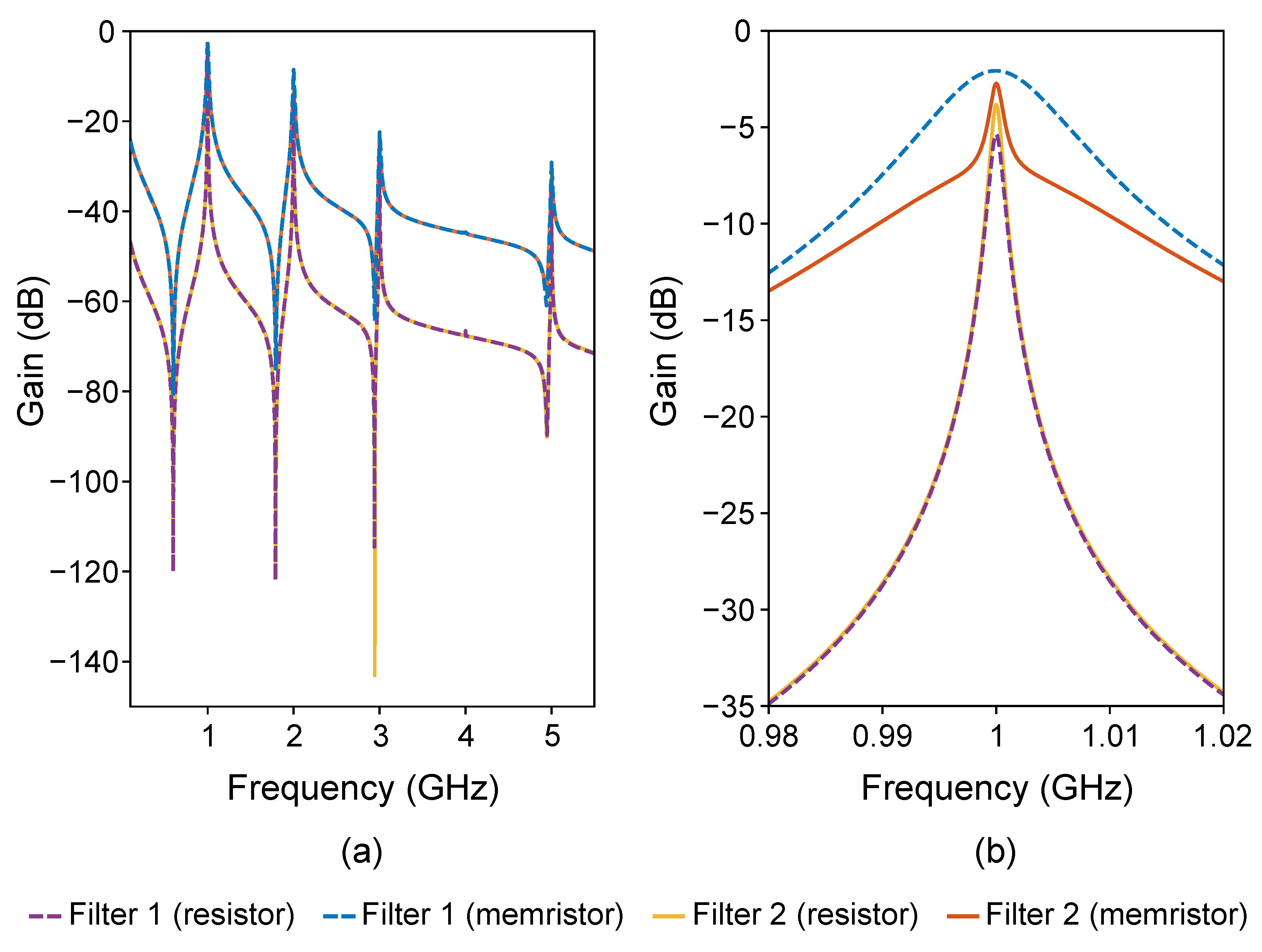
3.1. Simulation Results with 1 MHz Centre Frequency

The gains of the circuits built with a normal resistor and memristor and with different filter structures (normal N-path filter (Figure 2a) and Filter 1 (Figure 2b) structure) are shown in Figure 3. According to the simulation results, the gain responses of Filter 1 and Filter 2 were nearly identical at a centre frequency of 1 MHz. To ensure a great enough visual distinction for the different curves in Figure 2, only the gain curves of the original N-path filter and Filter 1 are presented. The results were simulated with a resistor and memristor at 10 k Ω , capacitors at 6 nF, and a 1 MHz switch frequency. The capacitor value was chosen to make the Q factor of the filter around 1000, which resulted in balanced selectivity and insertion loss. It could be found that in addition to the gain pass band at 1 GHz, there were extra gain peaks at 2 GHz, 3 GHz, and 5 GHz. These were the second, third, and fifth harmonic frequencies of the fundamental frequency. Referring to the normal N-path filter structure (Filter 1 with a resistor), when the input signal frequency was equal to twice the switching frequency ( f i n = 2 f s ), S1 and S3 would always record the average value of the positive cycle of the sine wave and S2 and S4 would always record the value of the negative cycle of the sine wave; hence, the gain at f i n = 2 f s was also high compared to for the other frequencies. The same thing happened when f i n was equal to 3 f s and 5 f s . However, when f i n = 4 f s , every switch recorded the average value of a whole sine wave cycle, which equalled 0 V [21]. Because of this, there is no gain peak at 4 GHz in Figure 3. For the filter structure with a resistor, the original N-path filter structure had a weaker stopband rejection level (at around −28 dB) compared with Filter 1 (at around −65 dB) but also had a simplified circuit structure which reduced the number of switches. However, when replacing the resistor with a memristor, the results show that the stopband attenuation floor of the gain in the original N-path filter structure will continue to increase with the frequency, which means that the original N-path filter with the memristor works as a high-pass filter at a high frequency. In Filter 1, the memristor results showed a weaker stopband rejection level (around −50 dB at the fourth harmonic position) compared with the resistor results (around −65 dB), but the rejection level of the curve with the memristor maintained a constant value smaller than −40 dB. The comparison results show that Filter 1 is more suitable for combination with a memristor to generate a reconfigurable device in comparison with the original N-path filter shown in Figure 2a.
The simulation gain values of the four-path filter at 1 MHz with Filter 1, 6 nF capacitors, and different memristor values are shown in Figure 4. The results show the centre frequency was not accurately 1 MHz but changed to 999.7 KHz. This small centre frequency shift was caused by the parasitic capacitance C p of the memristor. As the existence of C p increases the total capacitance in the RC network of the filter, it affects the time constant of the circuit, reduces the cut-off frequency, and thus shifts the centre frequency to a lower value. The larger the C p , the larger the centre frequency shift. The maximum gain of the curves with varying memristor values had around a 0.5 dB difference, which was caused by the change in the ratio between the memristor value and the ON state resistance of the switches. The larger the ratio [ R m e m r i s t o r / R s w i t c h ], the smaller the maximum gain. The trends of the curves in Figure 4 are the same as expected, and detailed data are recorded in Table 2. As Table 2 shows, for a four-path filter that works at around 1 MHz with an original quality factor, Q, of around 1000, a memristor with a resistance range of [10, 17] k Ω can generate a tuneable cut-off frequency range of [954, 1191] Hz, resulting in a tuneable quality factor range of [839, 1048]. When maintaining a constant Q factor of 1000, with a change in the memristor value, the centre frequency can change in the range of [0.95, 1.19] MHz. Compared with the original centre frequency of 1 MHz, the achievable rate of change of the centre frequency without Q factor variation is around 24%. The actual cut-off frequency when using a memristor is different from the f 3 d B when using a resistor. The differences are caused by the parasitic capacitance C p of the memristor. Referring to Equations (3) and (9), C p changes the impedance of the memristor when the frequency is high, increases the f 3 d B value, and reduces the tuneable f 3 d B range. As shown in Equation (9), when the frequency tends to infinity, the transfer function is no longer decided by the memristor resistance, which means that the f 3 d B value is not adjustable. The noise floor of Filter 1 with a memristor at a 1 MHz centre frequency is around −87 dB. Changing the memristor resistance will not cause a large difference in the noise floor value.
As the minimum step in the memristor resistance programming is ideally 1% of the current value, the minimum bandwidth tuning steps at different memristor values are recorded in Table 3. It can be found that the minimum bandwidth tuning step is smaller than 6.7 Hz, which means that this tuneable filter has a very small bandwidth step(smaller than 2.7% of the whole tuneable bandwidth range).

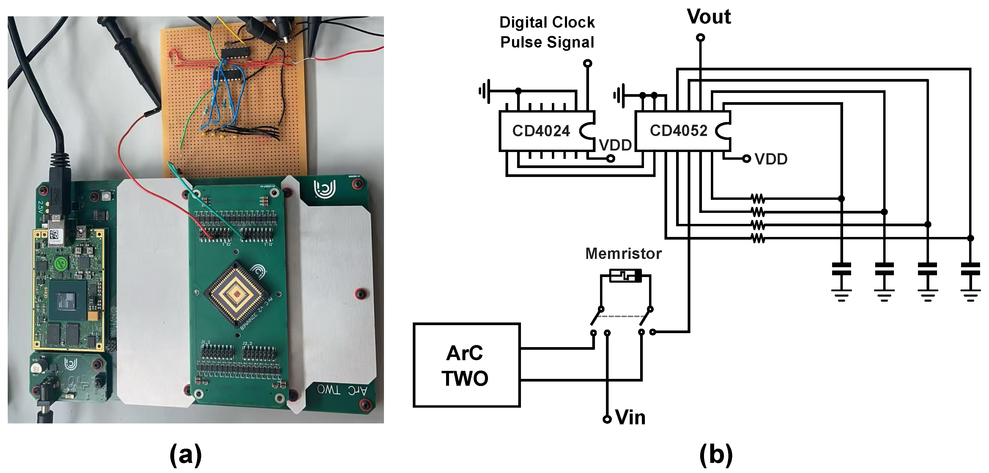
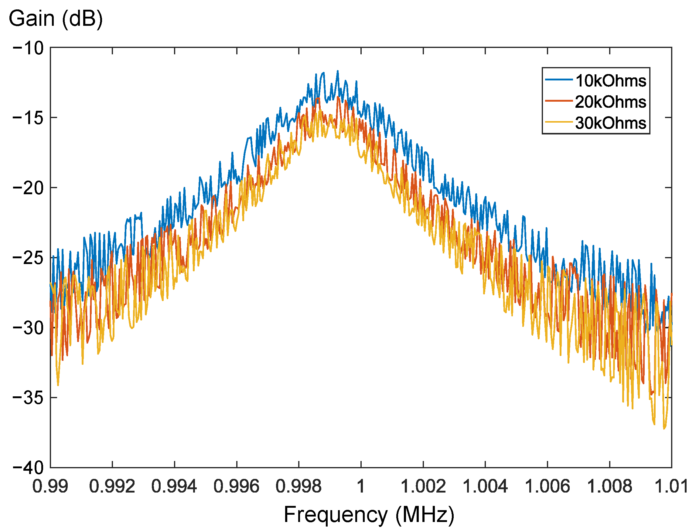
3.2. Measurement Results with Filter 1 Structure and 1 MHz Centre Frequency

The memristor package used in the laboratory measurement was a T i O x / A l 2 O 3 device [29]. The electrode overlap area of one memristor in the package was 10 × 10 µm2, and the thickness of the material in between the overlap electrodes was 4nm. The memristor package was programmed using ArC Two, which is a measurement instrument for working with RRAM arrays [40,41]. The memristor package was first integrated with an ArC Two daughter board, was programmed to the desired resistance, and then was placed on a break-out board and connected to the four-path filter. The memristor chosen to be combined with the four-path filter had a [10, 30] k Ω tuneable resistance range. A CD4024B CMOS ripple-carry binary counter combined with a waveform generator was used to generate the switches’ control signals. A CD4052B analog multiplexer was used as the four switch groups. Four small resistors were used to generate the ON resistance from the input signal part. As the memristor package was programmed using ArC Two, the switch S_P and V r e f were not included in the stripboard circuit. The capacitors used in the measurement were 6nF. The centre frequency of the multiplexer was set to 1MHz. A picture of the four-path filter on the stripboard with the memristor package is shown in Figure 5a, while a schematic of the circuit is shown in Figure 5b.
The measured transient waveform of the input sine wave and output of the four-path filter with a 10 k Ω memristor is shown in Figure 6a. The red dotted lines show the speculated output DC voltage level based on the output curve. Combining the input curve with the speculated output voltage values, it can be observed that one period of the input sine wave was sampled to four DC voltage values by the four-path filter. The output curve was noisy compared with the ideal voltage steps, and additionally, unwanted voltage drops between constant voltage levels could be observed in the measured output curve. The first reason for this was the switching time of the counter and multiplexer. In the simulation, the switches turned on/off without any delay or rise/fall time. However, in reality, it was found from the datasheets that the counter had an output Q n to Q n + 1 switching delay of 40 ns, while both the counter and the multiplexer has a rise and fall time of 20ns. Because of that, there was around an 80ns switching time during the turning on of the switches, which was close to the switching gaps observed in Figure 6a. Second, in the ideal condition when the input frequency equals the centre frequency, the voltage on each capacitor is constant. However, in practical measurements, it is not possible to precisely match the input signal frequency to the centre frequency. The higher the frequency, the larger the error of frequency matching. Because of that, in the measurement, the voltages on the capacitors in the four-path filter changed continually. When one group of switches turned on, the voltage on the corresponding capacitor underwent a period of oscillation before stabilizing. These two factors made the voltage unstable during the switching times.
Figure 6b compares the gain–frequency responses when using a 10 k Ω resistor and memristor. It can be found that the curves of the four-path filter when used with a resistor and memristor were similar. Both of the two curves had an average stopband rejection level of around −30 dB. At the centre frequency, the maximum gain when using a memristor was larger than in the condition using a resistor, which was because the parasitic capacitance reduced the impedance of the memristor; hence, the impedance of the memristor at 1 MHz was not actually 10 k Ω but a lower value. Also, at the second harmonic frequency, which was 2 MHz, the difference between the gains when using a memristor or a resistor was larger, as the impedance of the memristor was further reduced.
The gain curves of the four-path filter at a 1MHz centre frequency with different memristor values are shown in Figure 7. The gain values fluctuated sharply at similar frequencies, which was caused by the noise in the output signal, as shown in Figure 6a. Comparing Figure 7 with Figure 4, it can be found that the trend of the curve in the measurement results was the same as in the simulation results. Detailed data on the measured f 3 d B , the Q factor, and the tuneable f c range when maintaining a constant Q factor value are recorded in Table 4. The f 3 d B at memristor values of 20 k Ω and 30 k Ω was similar, while the f 3 d B at memristor values of between 10 k Ω and 20 k Ω had relatively large variation. This was mainly because the parasitic capacitance had a greater impact on reducing the impedance when associated with a larger resistor. In the mathematical simulation, with a 10 pF parasitic capacitance at 1 MHz, a 10 k Ω memristor had an 8.5 k Ω impedance and a 20 k Ω memristor had a 13 k Ω impedance, but a 30 k Ω memristor only had a 14 k Ω impedance. Comparing the data in Table 4 with those in Table 2, it was found that the measured f 3 d B values were larger overall than the simulation results. This shows that the parasitic capacitance in the measurement was larger than the value of 10 pF in the simulation. The Q factor in the measurement was small and could not reach 1000; hence, the tuneable f c range was set at a Q of 600. With a constant Q at 600, the f c could change in the range of [0.9, 1.2] MHz without varying the cut-off frequency.
The measurement results show there was a larger parasitic capacitance in the actual memristor device compared with the simulation, and the curves in the measurement results were noisy. One of the reasons for this was the interference from the stripboard and laboratory surroundings. The components on the stripboard used solid electrical wires for connection, which was bad for high-frequency signal transmission. It was observed that when moving the probes between the oscilloscope and stripboard during the measurement, the noise conditions of the transient curves also changed, which means that the laboratory environment could affect the measurement results. On the other hand, as the memristor package had to be placed on a specific break board, the connection between the signal source, memristor, and four-path filter was also based on long jumping cables, which had large parasitic components and large high-frequency-signal distortion.
Due to the noisy curves of the gain–frequency response, the bandwidth variation was hard to observe when the change in the memristor resistance was small. Because of this, the minimum bandwidth tuning step was not measured for the memristor package and four-path filter on the stripboard. The power consumption of the four-path filter was 38 mW. The energy was mainly used to sustain the operation of the binary counter and multiplexer. As the binary counter and multiplexer needed a 10 V voltage supply, the power consumption of the circuit was also large.

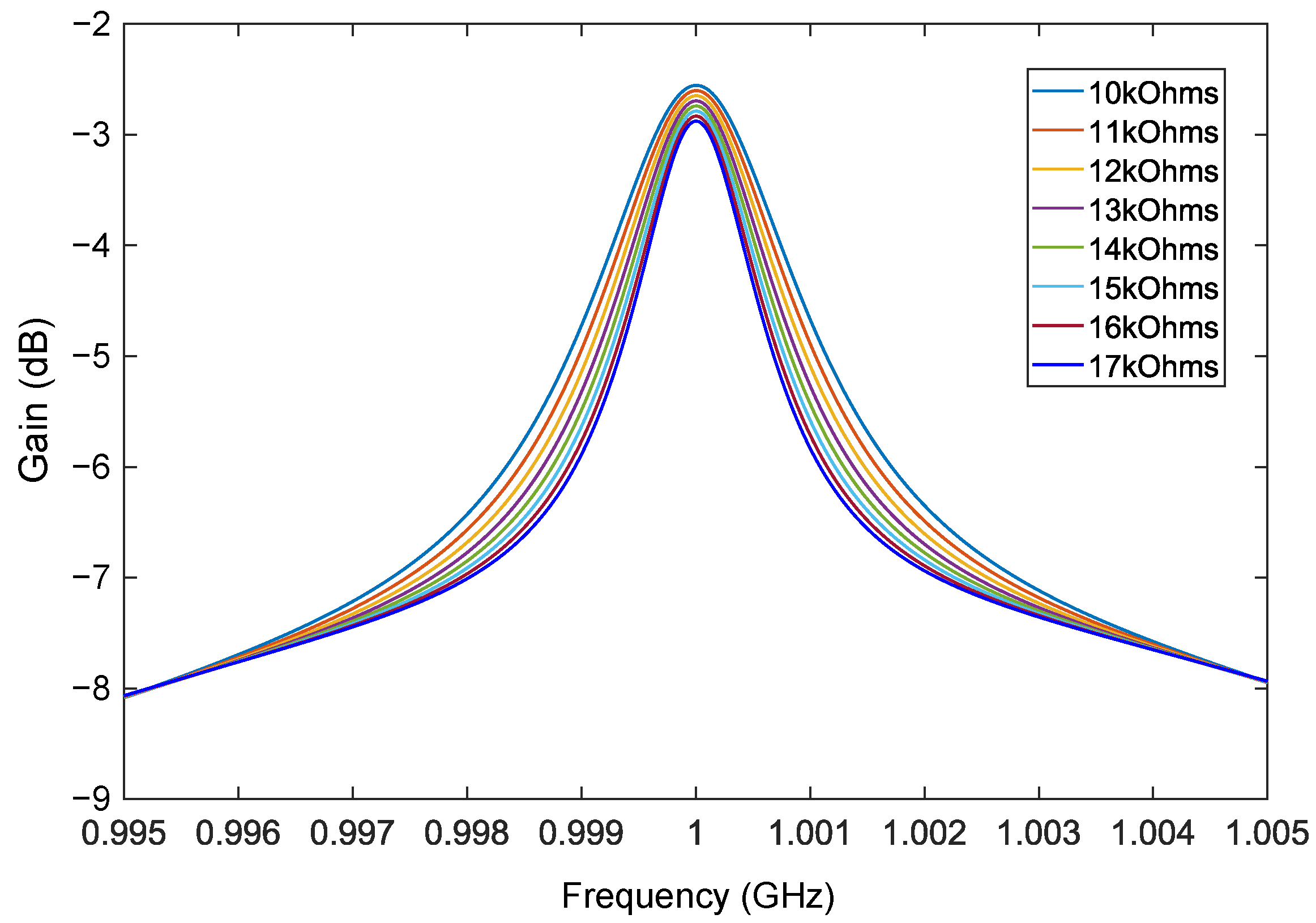
3.3. Simulation Results with Filter 2 Structure and 1 GHz Centre Frequency

Figure 8 compares the gain curves of the Filter 1 and Filter 2 structures with a memristor or resistor at a 1 GHz centre frequency. It can be observed from Figure 8a that, first, the two curves generated by memristor-based filters nearly overlapped, while the two curves generated by resistor-based filters also overlapped, and second, the resistor curves had stronger stopband rejection levels (at around −65 dB) and a narrower bandwidth compared with the memristor curves (with around a −45 dB rejection level). This means that using memristors in these structures with high-frequency signals can cause a low rejection ratio in the unwanted signal frequency range. Figure 8b shows that the [Filter 1 + memristor] curve had a wider bandwidth compared with the [Filter 1 and 2 + resistor] curve. The [Filter 2 + memristor] curve had a narrow bandwidth, which was similar to the [Filter 1 and 2 + resistor] curve when the input frequency was close to the centre frequency, but the bandwidth became larger and more similar to the [Filter 1 + memristor] curve when the input frequency was far from the centre frequency. This result shows that the memristors in Filter 2 could work as resistors when the input frequency was close to the centre frequency of the filter.
Referring to the concept of Filter 2 described in the Methodology Section, when the input frequency is the same as the centre frequency of the N-path filter, signals travelling through the memristors and capacitors approach constant DC voltages. However, when the input frequency is different from the centre frequency, the voltages on the capacitors will change whenever the switches turn on. The larger the difference between the input signal frequency and the switch centre frequency, the faster the voltages on the capacitors change. Because of that, only when the input signal frequency is very close to the centre frequency can the memristors work in baseband environments, which makes the gain curve have a narrow bandwidth similar to that in a condition using resistors. When the input frequency is far from the centre frequency, memristors work in high-frequency environments; hence, the curves of [Filter 1 + a memristor] and [Filter 2 + a memristor] were similar at these frequencies, as shown in Figure 8.
Figure 9 shows the simulation results for Filter 2 at a 1 GHz centre frequency with capacitor values of C = 8 pF and switches of R o = 800 Ω . Comparing Figure 9 with Figure 4, it can be found that the downward trend for the curves seen in Figure 9 slowed down at frequency far from the centre frequency f c . Also, at a frequency far away from the f c (lower than 996 MHz and higher than 1.001 GHz), the gain values of all the curves converged to the same value regardless of the memristor value. This was because the parasitic capacitor still dominated the memristor impedance at frequencies that were too far away from the f c and made the memristor value variation lose its original function. The frequency at which curves converged together was decided by the C p . The detailed data in Figure 9 are recorded in Table 5. The f 3 d B values when using memristors were higher than the f 3 d B values when using resistors. Contrary to the assumption that memristors work in ideal DC conditions when they are placed in between switch groups, the results show that the memristor impedance was still affected by the parasitic capacitor C p . However, the influence of C p in Filter 2 was much smaller than in Filter 1. For the gain results for Filter 1 at 1 GHz, no variation could be observed between different curves with varying memristor values. For Filter 2, Table 5 shows that the f 3 d B value could vary in a range of [0.99, 1.38] MHz, which resulted in a tuneable Q factor range from 725 to 1010 and a tuneable f c range of [0.99, 1.38] GHz when maintaining the Q factor at 1000. The achievable rate of change for f c without changing the Q factor was 39%, which was even better than the result for Filter 1 at 1 MHz. The noise floor of Filter 2 with a memristor at a 1 GHz centre frequency was around −92 dB. Compared with the result for Filter 1 at 1 MHz, the noise floor remained nearly the same, which may have been because the components used in the simulation were all ideal elements.
The minimum bandwidth change steps of the Filter 2 circuit at 1 GHz with different memristor values are recorded in Table 6. Due to the large centre frequency and small bandwidth change step, the bandwidth step values are not absolutely precise, but the trend of the bandwidth step changes can still be observed. The Filter 2 circuit had a minimum bandwidth change step smaller than 8.4 kHz, which meant it could tune the bandwidth with a step smaller than 2.2% of the whole tuneable bandwidth range. Similarly to the Filter 1 circuit at 1 MHz, the Filter 2 circuit operating at 1 GHz also showed the ability for very fine bandwidth tuning.

4. Discussion

The N-path filter is designed for high-frequency applications. However, the influence of the parasitic capacitance of the memristor in the filter increases with the frequency, which limits the operation of this memristor-based N-path filter at high frequencies. When simulating the Filter 1 circuit with a 10 pF parasitic capacitance, C p , and a 1 GHz centre frequency, f c , the variation in the memristor value nearly did not change the cut-off frequency of the filter, as at frequencies of up to 1 GHz, the impedance of the memristor was dominated by the fixed C p value instead of the tuneable memristor resistance.
The circuit with a Filter 2 structure solves the problem of designing a high-frequency memristor-based reconfigurable N-path filter. However, it also some some limitations. The main drawback of the Filter 2 circuit is the high quantity of memristors being used. The required amount of memristors equals the number of paths in the N-path filter, which will be a large value for a high-precision N-path filter. Only one memristor can be programmed in one programming process; hence, for a memristor-based four-path filter, the memristor programming process needs to be performed four times to change all the memristors to a specific value, which increases the complexity of operation. Furthermore, it is hard to program all the memristors to the same accurate resistance. The resistance difference between memristors in each path will reduce the accuracy of the output waveform. On the other hand, for an N-path filter that works with a 17 k Ω resistor, to achieve Q = 1000, the capacitor value needs to be around 5 pF. A reduction in the capacitor value increases the f 3 d B , but the frequency at which curves converge together is decided by C p , as shown in Figure 9, which is nearly constant. When using a memristor with C p = 10 pF, capacitors with a capacitance that is too small will make f 3 d B close to the convergence frequency, which will reduce the tuneable f 3 d B range. When f 3 d B is larger than the convergence frequency, the filter will lose the function of f 3 d B adjustment. Because of that, the f 3 d B value of Filter 2 at 1 GHz was limited to around 2 MHz or below. It can also be found from Figure 9 that the maximum f 3 d B variation range was located in the frequency range between around 998 kHz and 999 kHz, and the location of this [maximum f 3 d B range] remained almost unchanged with the variation in C. This means that when using larger capacitors, C, the tuneable f 3 d B range will be reduced. As a result, when using 16 pF capacitors instead of the 8 pF capacitors shown in Figure 9 and Table 5 to simulate the Filter 2 circuit, the tuneable f 3 d B range is reduced to [450, 671] kHz.
In the Results Section, the memristor model was assumed to have a 10 pF parasitic capacitance. This is a relatively high hypothetical value. The memristor packages used in the measurement had an electrode area of 10 × 10 µm2 for each memristor, which is also not the smallest area memristor manufacturing techniques can achieve. With more advanced manufacturing processes, memristors can have a smaller size and also a smaller parasitic capacitance [42]. Table 7 shows the results for f 3 d B and the Q factor with [Filter 1] and [Filter 2] circuit structures and different memristor C p values. All the values were simulated with R o = 800 Ω and C = 3 pF. It can be observed that for the Filter 1 circuit at a 1 GHz f c , with a high C p value, the bandwidth could not be maintained at a small value. When the C p increased, the bandwidth value increased but the tuneable bandwidth range decreased. Referring to Equation (2), high frequency and C p values reduce the impedance of the memristor (R value in Equation (2)), which limits the range of the bandwidth. Table 7 shows that with a C p at around 10 fF, the tuneable bandwidth range was similar to the condition that used a tuneable resistor in the N-path filter. Differently from the results for Filter 1, the bandwidth of the Filter 2 structure was not affected too much by the parasitic capacitance value. With an increase in the parasitic capacitance value, the bandwidth values slightly rose, and the tuneable bandwidth ranges even expanded. This phenomenon can also be observed in Table 6. This may be because the memristors at different resistance levels had different time constants, which expanded the difference in the gain in a specific frequency range and hence expanded the tuneable cut-off frequency range. Although this can not be observed from the table, a reduction in the C p improved the noise floor in the stopband of the Filter 2 structure N-path filter.
A comparison between the memristor-based N-path filters and other reconfigurable bandpass filters is shown in Table 8. The table does not fully show the performance advantages of the two memristor-based N-path filters introduced in this work when compared to other reconfigurable filters. This is primarily because the focus of this study was to demonstrate the feasibility and basic behaviour of integrating memristors into N-path filter structures. In the current stage of this research, no local oscillator or switch array circuits have been specifically designed to tune the centre frequency of the N-path filters. As all simulations were based on ideal switching components and frequency control in the Cadence Virtuoso environment, the range of the centre frequency and the power consumption cannot be listed in this table. Additionally, the use of ideal components led to a lower noise figure (NF) for both filters compared to other designs. With the implementation of practical switching circuitry in future research, the actual NF values of these two filters are expected to increase. Finally, although the tuneable bandwidth range was mainly determined by the selected capacitors, the simulation results for Filter 2 (Figure 9) indicate that its bandwidth tunability was effective only within a limited range near the centre frequency. Therefore, Filter 2 does have a relatively narrow bandwidth range compared with other designs in the table. However, this does not reduce its suitability for being used in extremely narrowband applications, like precision spectrum sensing or aerospace communication.

5. Conclusions

This work reports the application of memristors in reconfigurable N-path filters whose cut-off frequency can be adjusted using the memristor value. The frequency responses of three types of memristor-based N-path filter circuit structures were compared. A memristor-based four-path filter was tested in the laboratory with a memristor package at a 1 MHz centre frequency. The simulation results for different memristor-based four-path filters at 1 GHz were also recorded.
The simulation results show that the reconfigurable four-path filter designed using Filter 1, shown in Figure 2, could work well at 1 MHz with a memristor value of [10 k, 17 k] Ω and that it had a tuneable f 3 d B range of [954, 1191] Hz and a tuneable Q factor range of [839, 1048], with a minimum bandwidth tuning step smaller than 2.7% of the whole tuneable bandwidth range. A Filter 1 structure four-path filter was built on a stripboard and tested with a memristor which had a [10 k, 30 k] Ω resistance. The four-path filter had a tuneable f 3 d B range of [1.5, 2] kHz and a tuneable Q factor range of [500, 667]. A N-path filter that used multiple memristors (Filter 2) and could work at 1 GHz was also designed. The simulation results show the Filter 2 structure N-path filter had a tuneable f 3 d B range of [0.99, 1.38] GHz, which meant it had a tuneable f c range of [0.99, 1.38] GHz when maintaining Q = 1000, with a minimum f 3 d B tuning step smaller than 2.2% of its whole tuneable bandwidth range. The research in this article shows the very fine bandwidth-changing ability of these memristor-based N-path filter structures.
In further work, first, the schematics and layout of the memristor-based N-path filter structures need to be designed. After that, the performance of the circuit structures in this research can be compared with other work. Second, in the measurements in this research, the four-path filter on the stripboard showed a large parasitic capacitance, which reduced the performance of the circuit when working with a 1 MHz centre frequency. To measure the performance of a memristor-based N-path filter at a MHz frequency, a circuit built on a PCB board is needed. Also, the connection between the memristor and the N-path filter should be achieved using a specific connector instead of jumping wires. Third, the memristor package used in this research included several memristors with different resistance ranges. However, it was hard to find four similar memristors that had the same resistance ranges and current–voltage characteristics. Because of that, Filter 2, shown in Figure 2c, was not tested in the laboratory with real memristor components. In the future, if there are suitable memristors, Filter 2 should also be tested with an RF PCB at a high frequency.

Author Contributions

Conceptualization, F.Y. and S.W.; data curation, F.Y.; methodology, F.Y.; supervision, S.W., A.S. and T.P.; writing—original draft, F.Y.; writing—review and editing, S.W., A.S. and T.P. All authors have read and agreed to the published version of the manuscript.

Funding

This research is funede by UKRI, grant number EP/R024642/1,2.

Data Availability Statement

Data is contained within the article.

Conflicts of Interest

The authors declare no conflict of interest.

References

  1. Park, S.Y.; Meher, P.K. Efficient FPGA and ASIC realizations of a DA-based reconfigurable FIR digital filter. IEEE Trans. Circuits Syst. II Express Briefs 2014, 61, 511–515. [Google Scholar] [CrossRef]
  2. Mohanty, B.K.; Meher, P.K. A high-performance FIR filter architecture for fixed and reconfigurable applications. IEEE Trans. Very Large Scale Integr. (VLSI) Syst. 2015, 24, 444–452. [Google Scholar] [CrossRef]
  3. Han, Z.; Kohno, K.; Fujita, H.; Hirakawa, K.; Toshiyoshi, H. MEMS reconfigurable metamaterial for terahertz switchable filter and modulator. Opt. Express 2014, 22, 21326–21339. [Google Scholar] [CrossRef] [PubMed]
  4. Kumar, N.; Singh, Y.K. RF-MEMS-based bandpass-to-bandstop switchable single-and dual-band filters with variable FBW and reconfigurable selectivity. IEEE Trans. Microw. Theory Tech. 2017, 65, 3824–3837. [Google Scholar] [CrossRef]
  5. Donelli, M.; Manekiya, M.; Tagliapietra, G.; Iannacci, J. A reconfigurable pseudohairpin filter based on MEMS switches. Sensors 2022, 22, 9644. [Google Scholar] [CrossRef]
  6. Wada, T.; Ogami, T.; Horita, A.; Obiya, H.; Koshino, M.; Kawashima, M.; Nakajima, N. A new tunable SAW filter circuit for reconfigurable RF. In Proceedings of the 2016 IEEE MTT-S International Microwave Symposium (IMS), San Francisco, CA, USA, 22–27 May 2016; IEEE: Piscataway, NJ, USA, 2016; pp. 1–4. [Google Scholar]
  7. Lu, X.; Galipeau, J.; Mouthaan, K.; Briot, E.H.; Abbott, B. Reconfigurable multiband SAW filters for LTE applications. In Proceedings of the 2013 IEEE Radio and Wireless Symposium, Austin, TX, USA, 20–23 January 2013; IEEE: Piscataway, NJ, USA, 2013; pp. 253–255. [Google Scholar]
  8. Chen, R.; Hashemi, H. Passive coupled-switched-capacitor-resonator-based reconfigurable RF front-end filters and duplexers. In Proceedings of the 2016 IEEE Radio Frequency Integrated Circuits Symposium (RFIC), San Francisco, CA, USA, 22–24 May 2016; IEEE: Piscataway, NJ, USA, 2016; pp. 138–141. [Google Scholar]
  9. Ruderman, A. Filter capacitance reduction in DC/DC step-down reconfigurable switched-capacitor converters by a balanced switching. In Proceedings of the 2012 13th International Conference on Optimization of Electrical and Electronic Equipment (OPTIM), Brasov, Romania, 24–26 May 2012; IEEE: Piscataway, NJ, USA, 2012; pp. 776–782. [Google Scholar]
  10. Franks, L.E.; Sandberg, I.W. An alternative approach to the realization of network transfer functions: The N-path filter. Bell Syst. Tech. J. 1960, 39, 1321–1350. [Google Scholar] [CrossRef]
  11. Klumperink, E.; Nauta, B.N. Path Filters and Mixer-First Receivers—A Review. IC Des. Insights-Sel. Present. CICC 2022, 2017, 221–264. [Google Scholar]
  12. Luo, C.; Gudem, P.S.; Buckwalter, J.F. A 0.2–3.6-GHz 10-dBm B1dB 29-dBm IIP3 tunable filter for transmit leakage suppression in SAW-less 3G/4G FDD receivers. IEEE Trans. Microw. Theory Tech. 2015, 63, 3514–3524. [Google Scholar] [CrossRef]
  13. Moschytz, G.S. Inductorless filters: A survey II. Linear active and digital filters. IEEE Spectr. 1970, 7, 63–75. [Google Scholar] [CrossRef]
  14. Lin, Z.; Mak, P.I.; Martins, R.P.; Lin, Z.; Mak, P.I.; Martins, R.P. Analysis and modeling of a gain-boosted N-path switched-capacitor bandpass filter. In Ultra-Low-Power and Ultra-Low-Cost Short-Range Wireless Receivers in Nanoscale CMOS; Springer: Berlin/Heidelberg, Germany, 2016; pp. 57–80. [Google Scholar]
  15. Xu, Y.; Kinget, P.R. A switched-capacitor RF front end with embedded programmable high-order filtering. IEEE J. Solid-State Circuits 2016, 51, 1154–1167. [Google Scholar] [CrossRef]
  16. Krishnamurthy, S.; Niknejad, A.M. Design and analysis of enhanced mixer-first receivers achieving 40-dB/decade RF selectivity. IEEE J. Solid-State Circuits 2019, 55, 1165–1176. [Google Scholar] [CrossRef]
  17. Bonner-Stewart, J.; Wilson, C.; Floyd, B.A. Tunable 0.7–2.8-GHz reflection-mode N-path filters in 45-nm SOI CMOS. IEEE Trans. Microw. Theory Tech. 2020, 68, 2343–2357. [Google Scholar] [CrossRef]
  18. Lien, Y.C.; Klumperink, E.A.; Tenbroek, B.; Strange, J.; Nauta, B. Enhanced-selectivity high-linearity low-noise mixer-first receiver with complex pole pair due to capacitive positive feedback. IEEE J. Solid-State Circuits 2018, 53, 1348–1360. [Google Scholar] [CrossRef]
  19. Luo, C.; Gudem, P.S.; Buckwalter, J.F. A 0.4–6-GHz 17-dBm B1dB 36-dBm IIP3 channel-selecting low-noise amplifier for SAW-less 3G/4G FDD diversity receivers. IEEE Trans. Microw. Theory Tech. 2016, 64, 1110–1121. [Google Scholar] [CrossRef]
  20. Chua, L. Memristor-the missing circuit element. IEEE Trans. Circuit Theory 1971, 18, 507–519. [Google Scholar] [CrossRef]
  21. Strukov, D.B.; Snider, G.S.; Stewart, D.R.; Williams, R.S. The missing memristor found. Nature 2008, 453, 80–83. [Google Scholar] [CrossRef]
  22. Korkmaz, A.; He, C.; Katehi, L.P.; Williams, R.S.; Palermo, S. Design of tunable analog filters using memristive crossbars. In Proceedings of the 2021 IEEE International Symposium on Circuits and Systems (ISCAS), Daegu, Republic of Korea, 22–28 May 2021; IEEE: Piscataway, NJ, USA, 2021; pp. 1–5. [Google Scholar]
  23. He, C.; Korkmaz, A.; Palermo, S.; Williams, R.S.; Katehi, L.P. Analog Signal Processing in High Frequency Circuits Using Crossbar Configurations. In Proceedings of the 2021 IEEE International Conference on Microwaves, Antennas, Communications and Electronic Systems (COMCAS), Tel Aviv, Israel, 1–3 November 2021; IEEE: Piscataway, NJ, USA, 2021; pp. 116–121. [Google Scholar]
  24. Waser, R.; Aono, M. Nanoionics-based resistive switching memories. Nat. Mater. 2007, 6, 833–840. [Google Scholar] [CrossRef]
  25. Kim, H.; Sah, M.P.; Yang, C.; Chua, L.O. Memristor-based multilevel memory. In Proceedings of the 2010 12th International Workshop on Cellular Nanoscale Networks and their Applications (CNNA 2010), Berkeley, CA, USA, 3–5 February 2010; IEEE: Piscataway, NJ, USA, 2010; pp. 1–6. [Google Scholar]
  26. Borghetti, J.; Snider, G.S.; Kuekes, P.J.; Yang, J.J.; Stewart, D.R.; Williams, R.S. ‘Memristive’switches enable ‘stateful’logic operations via material implication. Nature 2010, 464, 873–876. [Google Scholar] [CrossRef]
  27. Li, Q.; Salaoru, I.; Khiat, A.; Xu, H.; Prodromakis, T. Correlated resistive/capacitive state variability in solid TiO2 based memory devices. Appl. Phys. A 2017, 123, 1–5. [Google Scholar] [CrossRef]
  28. Trapatseli, M.; Cortese, S.; Serb, A.; Khiat, A.; Prodromakis, T. Impact of ultra-thin Al2O3−y layers on TiO2−x ReRAM switching characteristics. J. Appl. Phys. 2017, 121, 184505. [Google Scholar] [CrossRef]
  29. Stathopoulos, S.; Khiat, A.; Trapatseli, M.; Cortese, S.; Serb, A.; Valov, I.; Prodromakis, T. Multibit memory operation of metal-oxide bi-layer memristors. Sci. Rep. 2017, 7, 17532. [Google Scholar] [CrossRef] [PubMed]
  30. Pi, S.; Li, C.; Jiang, H.; Xia, W.; Xin, H.; Yang, J.J.; Xia, Q. Memristor crossbar arrays with 6-nm half-pitch and 2-nm critical dimension. Nat. Nanotechnol. 2019, 14, 35–39. [Google Scholar] [CrossRef] [PubMed]
  31. Pickett, M.D.; Williams, R.S. Sub-100 fJ and sub-nanosecond thermally driven threshold switching in niobium oxide crosspoint nanodevices. Nanotechnology 2012, 23, 215202. [Google Scholar] [CrossRef] [PubMed]
  32. Wang, C.; Si, Z.; Jiang, X.; Malik, A.; Pan, Y.; Stathopoulos, S.; Serb, A.; Wang, S.; Prodromakis, T.; Papavassiliou, C. Multi-state memristors and their applications: An overview. IEEE J. Emerg. Sel. Top. Circuits Syst. 2022, 12, 723–734. [Google Scholar] [CrossRef]
  33. Maheshwari, S.; Stathopoulos, S.; Wang, J.; Serb, A.; Pan, Y.; Mifsud, A.; Leene, L.B.; Shen, J.; Papavassiliou, C.; Constandinou, T.G.; et al. Design flow for hybrid CMOS/memristor systems—Part I: Modeling and verification steps. IEEE Trans. Circuits Syst. I Regul. Pap. 2021, 68, 4862–4875. [Google Scholar] [CrossRef]
  34. Manouras, V.; Stathopoulos, S.; Garlapati, S.K.; Serb, A.; Prodromakis, T. Frequency response of metal-oxide memristors. IEEE Trans. Electron Devices 2021, 68, 3636–3642. [Google Scholar] [CrossRef]
  35. Ghaffari, A.; Klumperink, E.A.; Soer, M.C.; Nauta, B. Tunable high-Q N-path band-pass filters: Modeling and verification. IEEE J. Solid-State Circuits 2011, 46, 998–1010. [Google Scholar] [CrossRef]
  36. Smith, B.D. Analysis of commutated networks. Trans. IRE Prof. Group Aeronaut. Navig. Electron. 1953, 21–26. [Google Scholar] [CrossRef]
  37. LePage, W.R.; Cahn, C.R.; Brown, J.S. Analysis of a comb filter using synchronously commutated capacitors. In Transactions of the American Institute of Electrical Engineers, Part I: Communication and Electronics; IEEE: Piscataway, NJ, USA, 1953; Volume 72, pp. 63–68. [Google Scholar]
  38. Fischl, R. Analysis of a commutated network. In IEEE Transactions on Aerospace and Navigational Electronics; IEEE: Piscataway, NJ, USA, 1963; pp. 114–123. [Google Scholar]
  39. Messaris, I.; Serb, A.; Stathopoulos, S.; Khiat, A.; Nikolaidis, S.; Prodromakis, T. A data-driven verilog-a reram model. IEEE Trans. Comput.-Aided Des. Integr. Circuits Syst. 2018, 37, 3151–3162. [Google Scholar] [CrossRef]
  40. Berdan, R.; Serb, A.; Khiat, A.; Regoutz, A.; Papavassiliou, C.; Prodromakis, T. A μ-controller-based system for interfacing selectorless RRAM crossbar arrays. IEEE Trans. Electron Devices 2015, 62, 2190–2196. [Google Scholar] [CrossRef]
  41. Serb, A.; Khiat, A.; Prodromakis, T. An RRAM biasing parameter optimizer. IEEE Trans. Electron Devices 2015, 62, 3685–3691. [Google Scholar] [CrossRef]
  42. Pi, S.; Ghadiri-Sadrabadi, M.; Bardin, J.C.; Xia, Q. Nanoscale memristive radiofrequency switches. Nat. Commun. 2015, 6, 7519. [Google Scholar] [CrossRef] [PubMed]
  43. Ghotbi, I.; Behmanesh, B.; Törmänen, M. A reconfigurable RF filter with 1%–40% fractional bandwidth for 5G FR1 receivers. IEEE Solid-State Circuits Lett. 2023, 6, 97–100. [Google Scholar] [CrossRef]
  44. Bu, S.; Hameed, S.; Pamarti, S. Periodically time-varying noise cancellation for filtering-by-aliasing receiver front ends. IEEE J. Solid-State Circuits 2020, 56, 928–939. [Google Scholar] [CrossRef]
  45. Bu, S.; Pamarti, S. A dual-channel high-linearity filtering-by-aliasing receiver front-end supporting carrier aggregation. IEEE J. Solid-State Circuits 2021, 57, 1457–1469. [Google Scholar] [CrossRef]
  46. Dong, C.; Ren, M.; Jiang, X. A Tunable Integrated N-Path Bandpass Filter. Mob. Netw. Appl. 2024, 29, 1196–1202. [Google Scholar] [CrossRef]
  47. Gao, Z.; Qian, C. Design of the Reconfigurable N-path Filter. In Proceedings of the 2022 International Conference on Microwave and Millimeter Wave Technology (ICMMT), Harbin, China, 12–15 August 2022; IEEE: Piscataway, NJ, USA, 2022; pp. 1–3. [Google Scholar]
Figure 1. (a) T i O 2 / T i O 2 x memristor structure [21], where D is the thickness of the memristor’s insulator layer and W is the thickness of the T i O 2 layer throughout the whole insulator structure. (b) A 3D-model of a memristor in between two electrodes. (c) A lumped element model of a memristor.
Electronics 14 01858 g001
Figure 2. (a) Original N-path filter structure. (b) One-memristor-controlled N-path filter structure (Filter 1). (c) Multi-memristor-controlled N-path filter structure (Filter 2).
Electronics 14 01858 g002
Figure 3. Simulation gain of the circuits with the original N-path filter (Figure 2a)/Filter 1 (Figure 2b) structures and with a resistor/memristor. The [original N-path filter + memristor] structure had a noise floor that increased with the frequency. The Filter 1 structure showed a better noise floor than that of the original N-path filter structure.
Electronics 14 01858 g003
Figure 4. Simulation gain of the Filter 1 circuit with different values for the memristor. The bandwidth value changed in the range of [0.954, 1.191] kHz.
Electronics 14 01858 g004
Figure 5. (a) Photo of ArC Two, the memristor package, and the stripboard. (b) Schematic of the test circuit. When programming the memristor, the memristor package was connected to ArC Two; when the N-path filter was in the working mode, the memristor package cut off the connection with ArC Two and connected with the filter circuit.
Electronics 14 01858 g005
Figure 6. (a) Transient measurement result for the input curve (blue line), output curve (orange line), and speculated output DC voltage value (red dotted line). (b) Gain curves of the 4-path filter when using a memristor and a resistor.
Electronics 14 01858 g006
Figure 7. Measurement gain of the four-path filter with different memristor values. With a memristor resistance of [10, 30] k Ω , the tuneable bandwidth range was [1.5, 2] kHz. The noisy gain curves were mainly caused by the switching of the multiplexer.
Electronics 14 01858 g007
Figure 8. (a) Simulation gain curve comparison results for Filter 1 and Filter 2 with a memristor and resistor in the [0, 5.5] GHz frequency range. When observed over a wide frequency range, the curves of Filter 1 and Filter 2 with memristors appeared nearly identical. (b) The gain curves for the three conditions in the [0.98, 1.02] GHz frequency range.
Electronics 14 01858 g008
Figure 9. Simulation gain curves for Filter 2 with different memristor values. The tuneable bandwidth range offered by the Filter 2 structure memristor-based 4-path filter was [0.99, 1.38] MHz.
Electronics 14 01858 g009
Table 1. V i n , V r e f , S_P, and switch group operations of memristor-based 4-path filter [Filter 1].
Normal OperationProgramming Mode 1Programming Mode 2
V i n 0.5V DC + signal2.5V pulse0V
V r e f 0V0V2.5V pulse
S_POFFONON
S1 to S4ON in sequenceOFFOFF
Table 2. Cut-off frequency ( f 3 d B ) and quality factor (Q) with different memristor values and centre frequency ( f c ) range when quality factor is maintained at 1000.
Memristor ( Ω ) f 3 dB with Resistor (Hz)Actual f 3 dB (Hz)Q Factor f c with Q = 1 k (Hz)
10 k110511918391.19 M
11 k105311408771.14 M
12 k100710959131.1 M
13 k96410599441.06 M
14 k93510279731.03 M
15 k906100010001 M
16 k8809751025975 k
17 k8579541048954 k
Table 3. Minimum f 3 d B tuning step at different memristor resistance values for the Filter 2 structure at 1 MHz f c .
Memristor ( Ω )10 k11 K12 k13 k14 k15 k16 k17 k
Min step (Hz)6.7554.54.53.443
Table 4. Measured f 3 d B and Q factor with different memristor values and f c range when Q factor was maintained at 600.
Memristor ( Ω ) f 3 dB (Hz)Q Factor f c with Q = 600 (Hz)
10 k2 k5001.2 M
15 k1.8 k5561 M
20 k1.6 k6250.96 M
30 k1.5 k6670.9 M
Table 5. f 3 d B and Q factor with different memristor values and f c range when Q factor was maintained at 1000 in Filter 2 circuit with 1GHz original f c .
Memristor ( Ω ) f 3 dB with Resistor (Hz)Actual f 3 dB (Hz)Q Factor f c with Q = 1 k (Hz)
10 k590 k1380 k7251.38 G
11 k543 k1310 k7631.31 G
12 k510 k1230 k8131.23 G
13 k480 k1170 k8551.17 G
14 k456 k1120 k8931.12 G
15 k436 k1070 k9351.07 G
16 k413 k1030 k9711.03 G
17 k395 k990 k10100.99 G
Table 6. Minimum f 3 d B tuning step at different memristor resistance values for Filter 2 structure at 1GHz f c .
Memristor ( Ω )10 k11 K12 k13 k14 k15 k16 k17 k
Min step (Hz)7k6.5k8.4k5.6k5k4k3k3.7k
Table 7. Bandwidth ( f 3 d B ) of Filter 1 and Filter 2 at 1 GHz with different parasitic capacitance values.
C p (F)Memristor ( Ω )Filter 1 f 3 dB (Hz)Filter 2 f 3 dB (Hz)
500 f10 k10.16 M3.01 M
17 k10.13 M1.98 M
100 f10 k3.24 M2.91 M
17 k3.1 M1.97 M
50 f10 k2.1 M2.33 M
17 k1.9 M1.88 M
10 f10 k1.2 M1.59 M
17 k946 k1.22 M
010 k1.11 M1.25 M
17 k865 k800 k
Table 8. Comparison between the memristor-based N-path filter and other reconfigurable bandpass filters.
Ref.Tech.Frequency [Hz]Bandwidth [Hz]Gain [dB]NF [dB]
[43]22 nm1.7∼6.4 G50∼120 0M18∼324.6∼7.4
[44]28 nm0.1∼1 G2.5∼40 M304.1∼5.8
[45]28 nm0.1∼1 G5∼20 M7.8∼1010.5∼14.1
[46]65 nm50∼100 M1.5∼45 M15/
[47]55 nm0.1∼1 G75∼119 M//
Filter 1 (simulation)180 nm1 M0.95∼1.2 k−7∼−62.1
Filter 2 (simulation)180 nm1 G0.99∼1.4 M−3∼−2.53.6
Disclaimer/Publisher’s Note: The statements, opinions and data contained in all publications are solely those of the individual author(s) and contributor(s) and not of MDPI and/or the editor(s). MDPI and/or the editor(s) disclaim responsibility for any injury to people or property resulting from any ideas, methods, instructions or products referred to in the content.

